
ECE 565 VLSI Chip Design Styles Shantanu Dutt


- Slides: 23
ECE 565 VLSI Chip Design Styles Shantanu Dutt ECE Dept. UIC
Chip Design Styles • Differentiation wrt basic logic block’s logic complexity, logic variety, and dimension variety, which determine both placement and routing complexity (programmability of the logic block and routing fabric is another defining factor, but it does not affect placement and routing is affected minimally): – – Gate Array Standard Cell Macro Cell Full Custom: Block/Cell and transistor aspect ratios, shape (need not be rectangular), floorplanning can be controlled by the designer to achieve a high degree of optimization—hand tuned designs – Field Programmable Gate Array (FPGA)
Gate Array Design Style
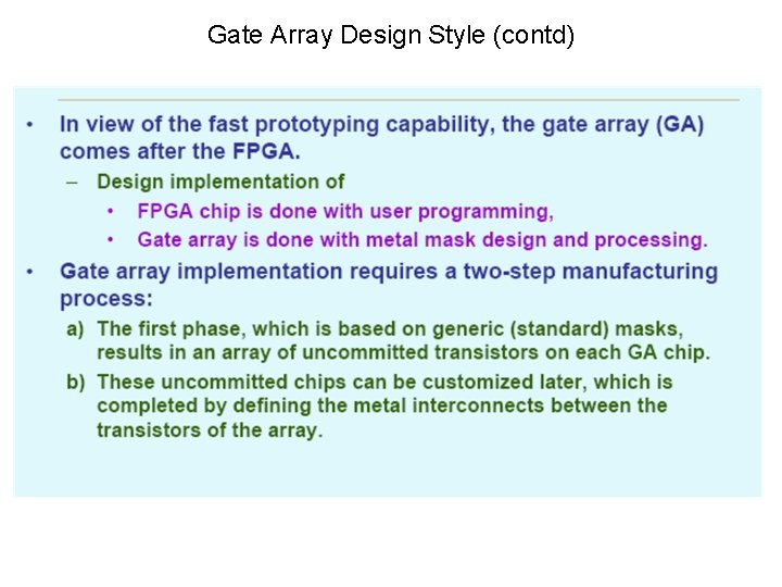
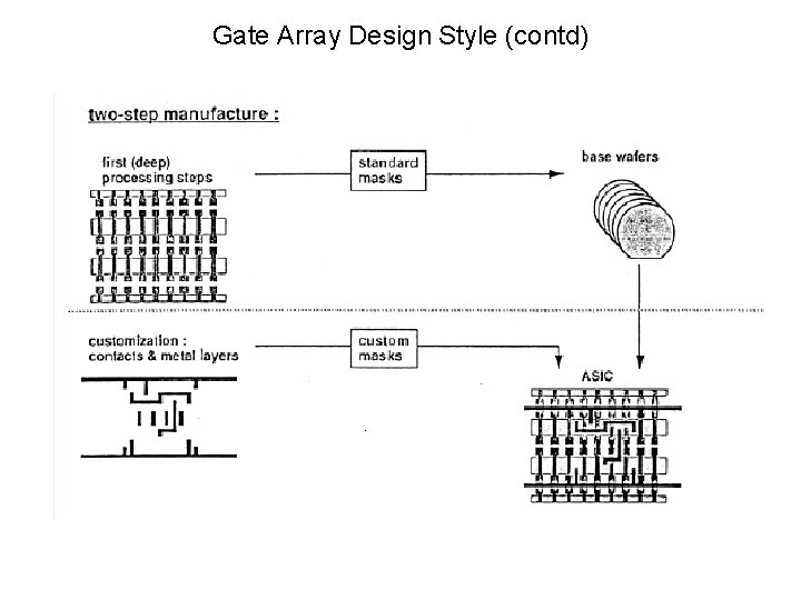
Gate Array Design Style (contd)
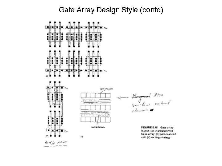
Gate Array Design Style (contd)
Gate Array Design Style (contd)
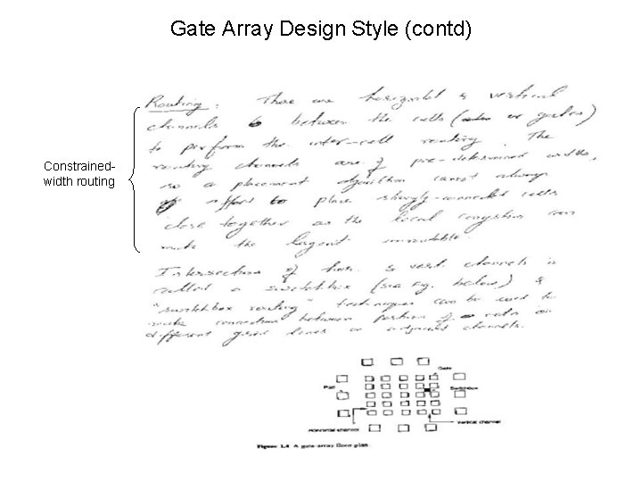
Gate Array Design Style (contd) Constrainedwidth routing
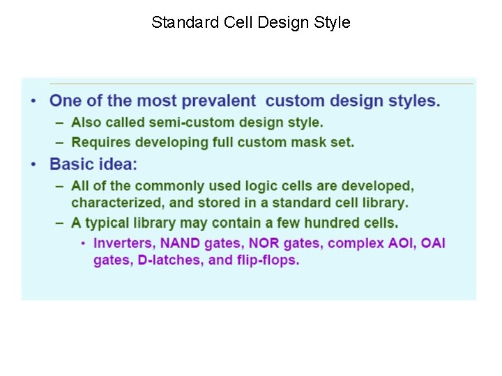
Standard Cell Design Style
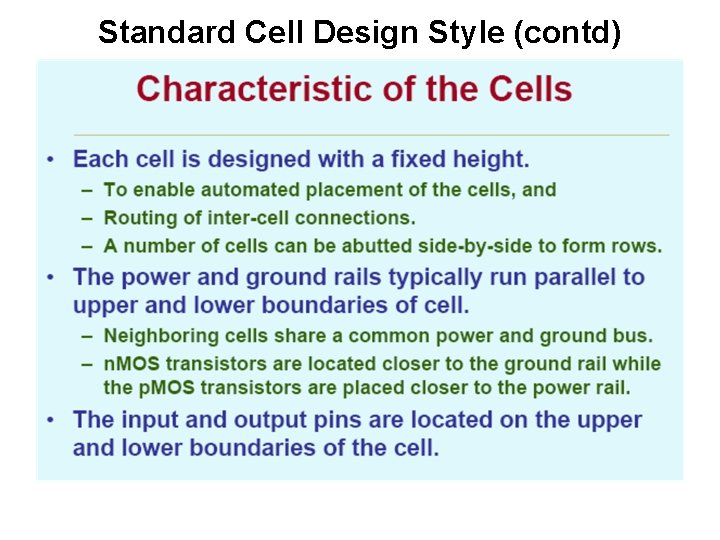
Standard Cell Design Style (contd)
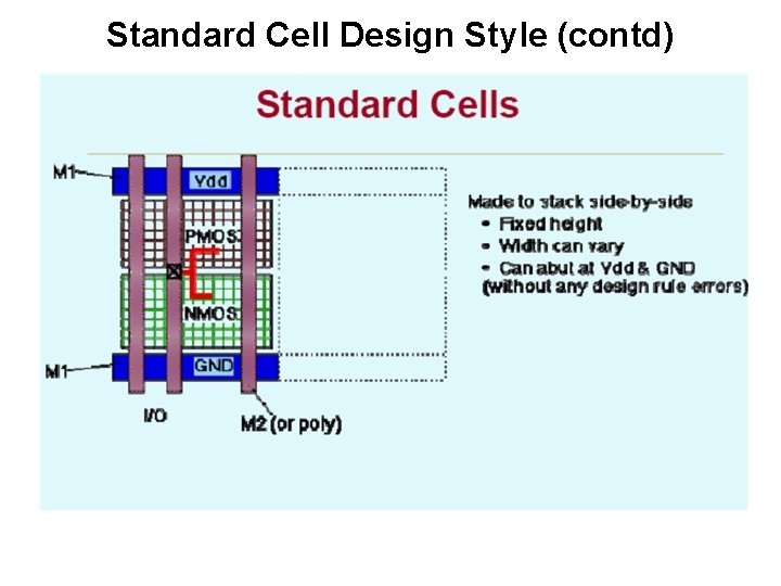
Standard Cell Design Style (contd)
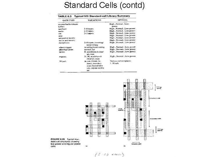
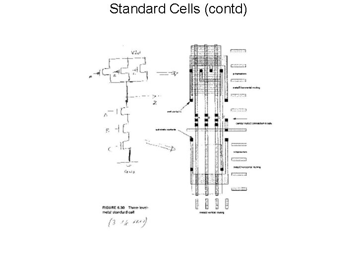
Standard Cells (contd)
Standard Cells (contd)
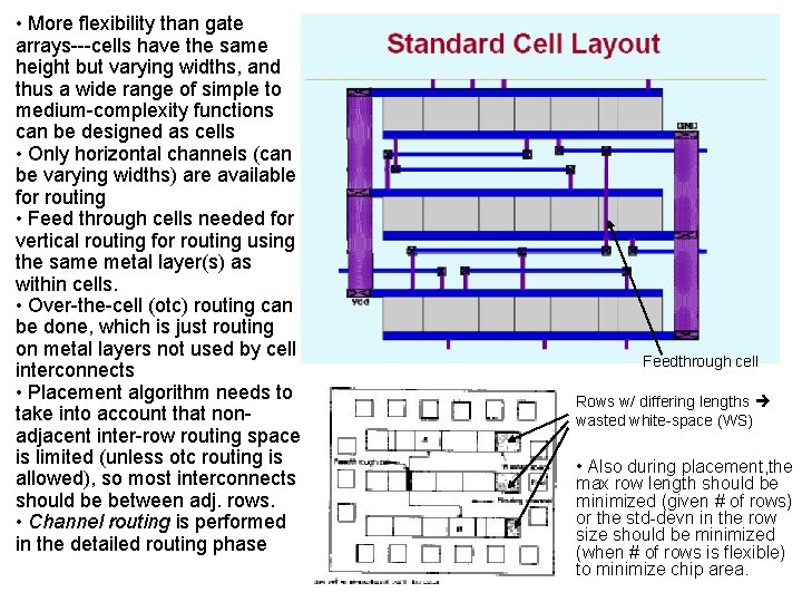
• More flexibility than gate arrays---cells have the same height but varying widths, and thus a wide range of simple to medium-complexity functions can be designed as cells • Only horizontal channels (can be varying widths) are available for routing • Feed through cells needed for vertical routing for routing using the same metal layer(s) as within cells. • Over-the-cell (otc) routing can be done, which is just routing on metal layers not used by cell interconnects • Placement algorithm needs to take into account that nonadjacent inter-row routing space is limited (unless otc routing is allowed), so most interconnects should be between adj. rows. • Channel routing is performed in the detailed routing phase Feedthrough cell Rows w/ differing lengths wasted white-space (WS) • Also during placement, the max row length should be minimized (given # of rows) or the std-devn in the row size should be minimized (when # of rows is flexible) to minimize chip area.
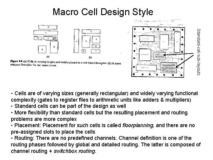
Macro Cell Design Style Standard-cell sub-layouts • Cells are of varying sizes (generally rectangular) and widely varying functional complexity (gates to register files to arithmetic units like adders & multipliers) • Standard cells can be part of the design as well • More flexibility than standard cells but the resulting placement and routing problems are more complex • Placement: Placement for such cells is called floorplanning, and there are no pre-assigned slots to place the cells • Routing: There are no predefined channels. Channel definition is one of the routing phases followed by global and detailed routing. The latter is composed of channel routing + switchbox routing.
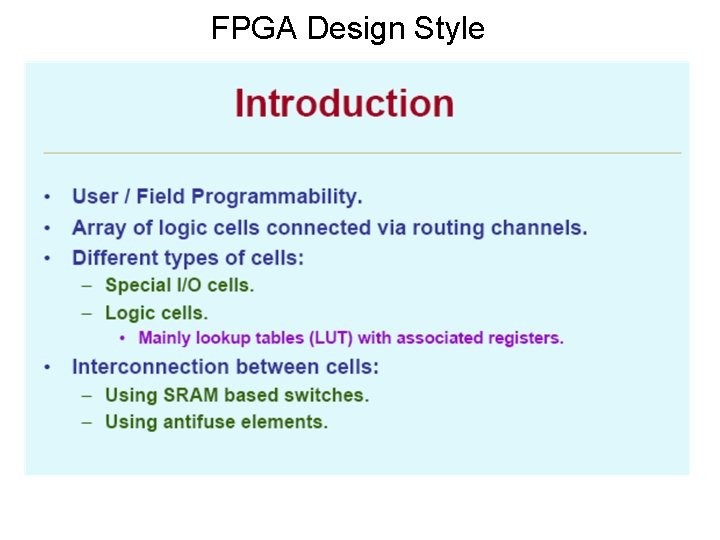
FPGA Design Style
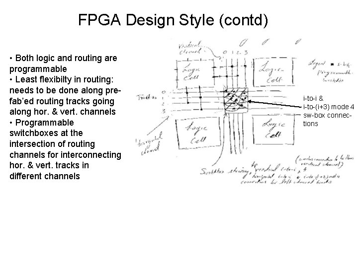
FPGA Design Style (contd) • Both logic and routing are programmable • Least flexibilty in routing: needs to be done along prefab’ed routing tracks going along hor. & vert. channels • Programmable switchboxes at the intersection of routing channels for interconnecting hor. & vert. tracks in different channels i-to-i & i-to-(i+3) mode 4 sw-box connections
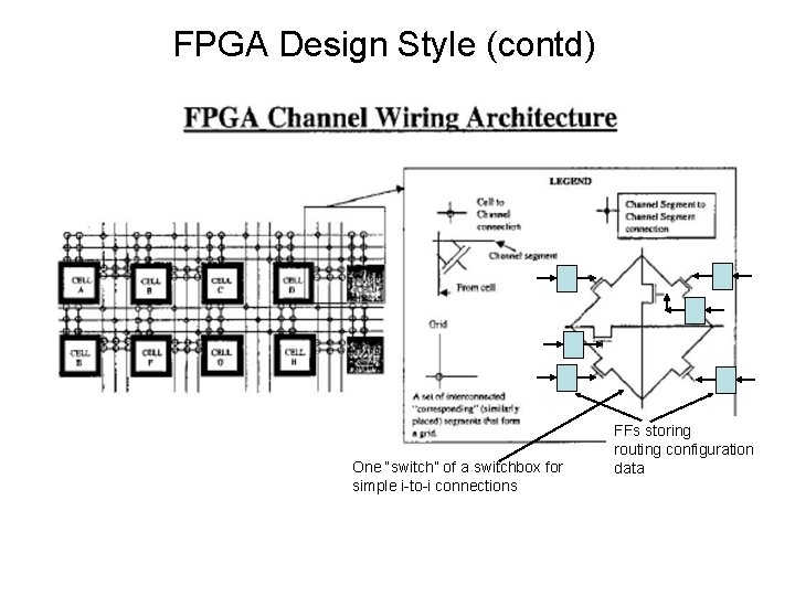
FPGA Design Style (contd) One “switch” of a switchbox for simple i-to-i connections FFs storing routing configuration data
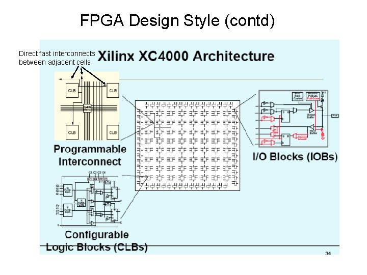
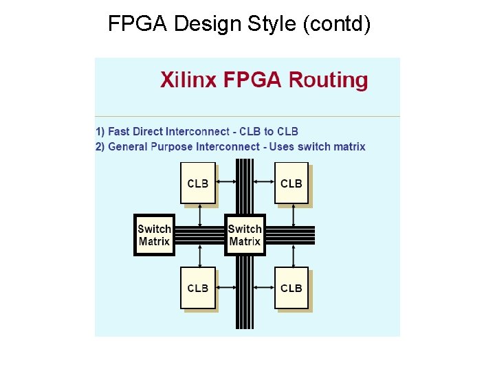
FPGA Design Style (contd) Direct fast interconnects between adjacent cells
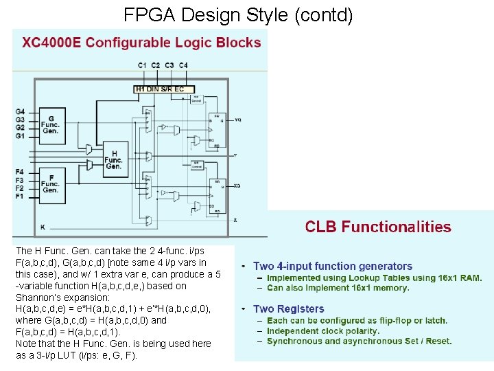
FPGA Design Style (contd) The H Func. Gen. can take the 2 4 -func. i/ps F(a, b, c, d), G(a, b, c, d) [note same 4 i/p vars in this case), and w/ 1 extra var e, can produce a 5 -variable function H(a, b, c, d, e, ) based on Shannon’s expansion: H(a, b, c, d, e) = e*H(a, b, c, d, 1) + e’*H(a, b, c, d, 0), where G(a, b, c, d) = H(a, b, c, d, 0) and F(a, b, c, d) = H(a, b, c, d, 1). Note that the H Func. Gen. is being used here as a 3 -i/p LUT (i/ps: e, G, F).
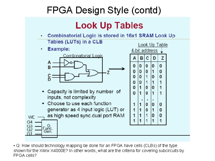
FPGA Design Style (contd) • Q: How should technology mapping be done for an FPGA have cells (CLBs) of the type shown for the Xilinx X 4000 E? In other words, what are the criteria for covering subcircuits by FPGA cells?
FPGA Design Style (contd)
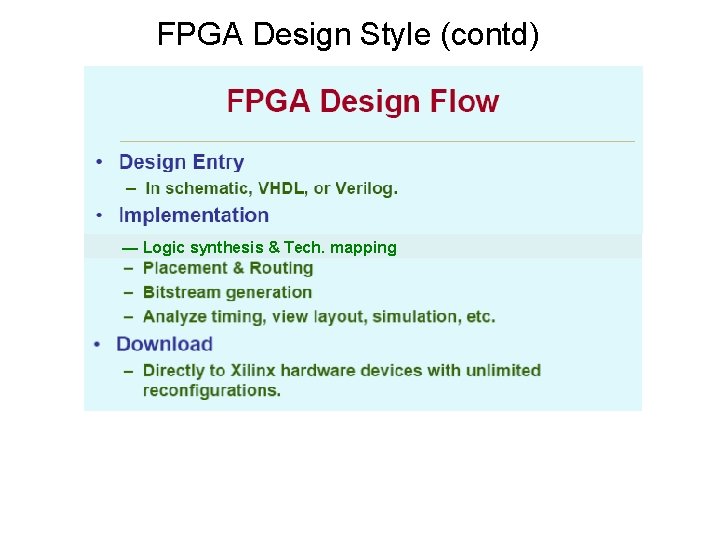
FPGA Design Style (contd) — Logic synthesis & Tech. mapping
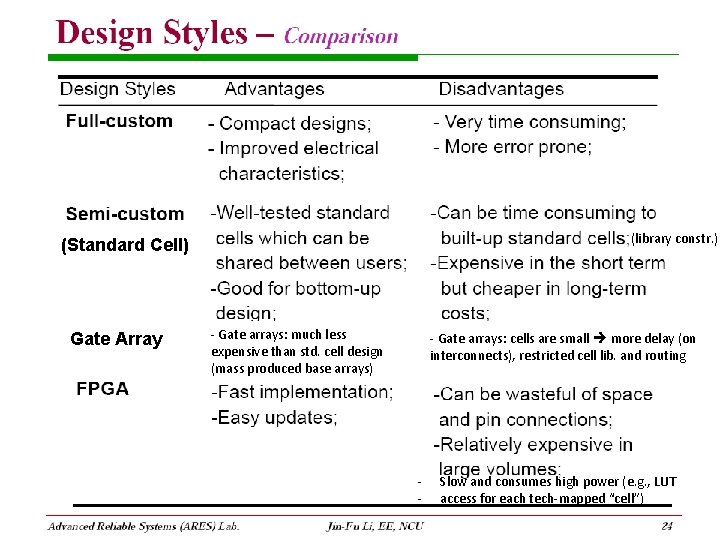
(library constr. ) (Standard Cell) Gate Array - Gate arrays: much less expensive than std. cell design (mass produced base arrays) - Gate arrays: cells are small more delay (on interconnects), restricted cell lib. and routing - Slow and consumes high power (e. g. , LUT access for each tech-mapped “cell”)