Chapter 1 VLSI Design Methodology Outline Introduction VLSI


")


 includes digital logic,")
, D flip flop and LUT. • LUT")

 is a programmable logic device with complexity")


 Pin Grid Array")
 • low cost ( Advantage) • dimensions can be prohibitive,")
 Packages • higher pin count (typically 100 to more than")
 • This SMT package type is available in two variations,")
 • This SMT package type is similar to leaded chip")
 • This IC package option can be used for special applications")


 used to reduce complexity of IC")
- Slides: 59
Chapter 1 VLSI Design Methodology
Outline • • • Introduction VLSI Design Flows & Design Verification VLSI Design Styles Design Hierarchy Concept of Regularity, Modularity and Locality
Moore's law • Moore's law is the observation that the number of transistors in a dense integrated circuit doubles about every two years GORDON MOORE
Table-1. 1: Evolution of logic complexity in integrated circuits. ERA DATE COMPLEXITY (number of logic blocks per chip) Single transistor 1959 less than 1 Unit logic (one gate) 1960 1 Multi-function 1962 2 - 4 Complex function 1964 5 -20 Medium Scale Integration 1967 20 -200 (MSI) Large Scale Integration 1972 200 -2000 (LSI) Very Large Scale Integration 1978 2000 -20000(VLSI) Ultra Large Scale Integration 1989 20000 - ? (ULSI)
Complexity & Productivity Growth of ICs • Complexity grows 58%/yr (doubles every 18 months) • Productivity grows 21%/yr (doubles every 3. 5 yrs) unless methodology is updated
VLSI Design Methodologies § • • • Design methodology Process for creating a design Methodology goals Design cycle Complexity Performance Reuse Reliability
IC Community
System to Silicon Design
Y-Chart
Y Chart • The design flow starts from the algorithm that describes the behavior of the target chip. • The corresponding architecture of the processor is first defined. • It is mapped onto the chip surface by floorplanning. • The next design evolution in the behavioral domain defines finite state machines (FSMs) which are structurally implemented with functional modules such as registers and arithmetic logic units (ALUs). • These modules are then geometrically placed onto the chip surface using CAD tools for automatic module placement followed by routing, with a goal of minimizing the interconnects area and signal delays. • The third evolution starts with a behavioral module description. • Individual modules are then implemented with leaf cells. • At this stage the chip is described in terms of logic gates (leaf cells), which can be placed and interconnected by using a cell placement & routing program. • The last evolution involves a detailed Boolean description of leaf cells followed by a transistor level implementation of leaf cells and mask generation. • In standard-cell based design, leaf cells are already pre-designed and stored in a library for logic design use.
VLSI Design Flow
Discuss VLSI Design flow in d
Design Styles • Full Custom Design • Semi Custom Design
Full Custom
Design Styles – Programmable Logic Array
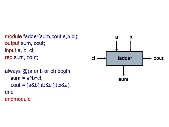
Standard-Cell Design Styles • Design entry • Enter the design into an ASIC design system, either using a hardware description language (HDL) or schematic entry • An example of Verilog HDL
Design Styles – Comparison Design Styles Advantages Disadvantages -Compact designs; - Improved electrical characteristics; Semi-custom -Well-tested standard cells which can be shared between users; -Good for bottom-up design; FPGA -Fast implementation; -Easy updates; -Very time consuming; - More error prone; Full-custom -Can be time consuming to built-up standard cells; -Expensive in the short term -Can be wasteful of space and pin connections; -Relatively expensive in large volumes;
General architecture of FPGA • The term FPGA stands for Field Programmable Gate Array and, it is a one type of semiconductor logic chip which can be programmed to become almost any kind of system or digital circuit, similar to PLDs. • PLDs are limited to hundreds of gates, but FPGAs supports thousands of gates. The configuration of the FPGA architecture is generally specified using a language, i. e. , HDL (Hardware Description language) which is similar to the one used for an ASIC ( Application Specific Integrated Circuit).
• FPGAs can provide a number of advantages over a fixed function ASIC technology such as standard cells. • Normally, ASICs takes months to manufacture and the cost of them will be thousands of dollars to obtain the device. • But, FPGAs are fabricated in less than a second, the cost will be from a few dollars to a thousand dollars. • The flexible nature of the FPGA comes at a significant cost in area, power consumption and delay. • When compared to a standard cell ASIC, an FPGA requires 20 to 35 times more area, and the speed’s performance will be 3 to 4 times slower than the ASIC.
FPGA Architecture
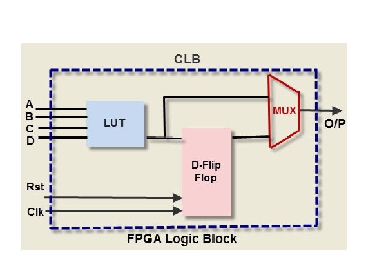
Functions of an FPGA architecture module • CLB (Configurable Logic Block) includes digital logic, inputs, outputs. It implements the user logic. • Interconnects provide direction between the logic blocks to implement the user logic. • Depending on the logic, switch matrix provides switching between interconnects. • I/O Pads used for the outside world to communicate with different applications.
• Logic Block contains MUX (Multiplexer), D flip flop and LUT. • LUT implements the combinational logical functions; the MUX is used for selection logic, and D flip flop. • The basic building block of the FPGA is the Look Up Table based function generator. • The number of inputs to the LUT vary from 3, 4, 6, and even 8 after experiments. • Now, we have adaptive LUTs that provides two outputs per single LUT with the implementation of two function generators.
• Xilinx Virtex-5 is the most popular FPGA, that contains a Look up Table (LUT) which is connected with MUX, and a flip flop as discussed above. • Present FPGA consists of about hundreds or thousands of configurable logic blocks. • For configuring the FPGA, Modelsim and Xilinx ISE softwares are used to generate a bitstream file and for development.
CPLD A complex programmable logic device (CPLD) is a programmable logic device with complexity between that of PALs and FPGAs, and architectural features of both. The main building block of the CPLD is a macrocell, which contains logic implementing disjunctive normal form expressions and more specialized logic operations.
CPLD Architecture
• A complex programmable logic device comprises of a group of programmable FBs (functional blocks). The inputs and outputs of these functional blocks are connected together by a GIM (global interconnection matrix). This interconnection matrix is reconfigurable, so that we can modify the contacts between the functional blocks. There will be some input and output blocks that let us to unite CPLD to external world. • Generally, the programmable FB looks like the array of logic gates, where an array of AND gates can be programmed and OR gates are stable.
CPLD • Some of the families of CPLD from different retailers include • Altera MAX 7000 and MAX 9000 families • Atmel ATF and ATV families • Lattice isp LSI family • Lattice (Vantis) MACH family • Xilinx XC 9500 family
COMPARISION OF FPGA AND CPLD No. CPLD FPGA 1 Instant-on. CPLDs start working as soon as they are powered up Since FPGA has to load configuration data from external ROM and setup the fabric before it can start functioning, there is a time delay between power ON and FPGA starts working. The time delay can be as large as several tens of milliseconds. 2 Non-volatile. CPLDs remain programmed, and retain their circuit after powering down. FPGAs go blank as soon as powered-off. FPGAs uses SRAM based configuration storage. The contents of the memory is lost as soon as power is disconnected. 3 Deterministic Timing Analysis. Since CPLDs are comparatively simpler to FPGAs, and the number of interconnects are less, the timing analysis can be done much more easily. Size and complexity of FPGA logic can be humongous compared to CPLDs. This opens up the possibility less deterministic signal routing and thus causing complicated timing scenarios. Thankfully implementation tools provided by FPGA vendors have mechanisms to assist achieving deterministic timing. But additional steps by the user is usually necessary to achieve this.
COMPARISION OF FPGA AND CPLD No. CPLD FPGA 4 Lower idle power consumption. Newer CPLDs such as Cool. Runner-II use around 50 u. A in idle conditions. Relatively higher idle power consumption. 5 Might be cheaper for FPGAs are much more capable compared to implementing simpler circuits CPLDs but can be more expensive as well. 6 More "secure" due to design FPGAs that use external memory can expose the storage within built in non. IP externally. Many FPGA vendors offer volatile memory. mechanisms such as encryption to combat this. Design specific protection mechanisms also can be implemented. 7 Very small amount of logic resources. Massive amount logic and storage elements, with which incredibly complex circuits can be designed. FPGAs have thousands times more resources! This point alone makes FPGAs more
COMPARISION OF FPGA AND CPLD No. CPLD FPGA 8 No on-die hard IPs available to offload processing from the logic fabric. Variety of on-die dedicated hardware such as Block RAM, DSP blocks, PLL, DCMs, Memory Controllers, Multi-Gigabit Transceivers etc give immense flexibility. This is not even thinkable with CPLDs. 9 Power down and reprogramming is always required in order to modify design functionality. FPGAs can change their circuit even while running! (Since it is just a matter of updating LUTs with different content) This is called Partial Reconfiguration, and is very useful when FPGAs need to keep running a design and at the same time update it with different design as per requirement. This feature is widely used in Accelerated Computing.
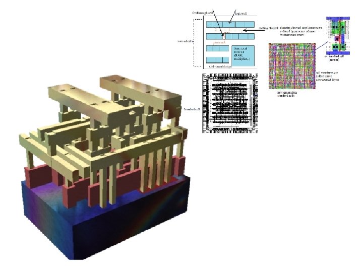
Standard Cell based Design • Commonly used logics are developed, characterized and stored in a standard cell library • Cell library includes: Ø Delay time versus load capacitance Ø Circuit simulation model Ø Timing simulation model Ø Fault simulation model Ø Cell data for place-and-route Ø Mask data
• Standard cell arrangement: Ø Fixed cell height Ø Parallel power and ground rails Ø Input and output pins are located on the upper and lower boundaries Ø Cells are placed side by side in standard-cell based design § The required logic circuits are realized using the cells in the library Ø Complete mask sets are developed for chip fabrication Ø One of the most prevalent design style for ASIC applications design
Design Quality • Testability Ø Time and effort for chip test increase exponentially with design complexity Ø The test task requires ü Generation of good test vectors ü Availability of reliable test fixture at speed ü Design of testable chip
Yield and manufacturability • The ratio of good tested chips to total tested chips • Functionality yield: Ø Testing the chips at lower speed Ø Identify problems of shorts, opens and leakage current Ø Detect logic and circuit design failure • Parametric yield Ø Test at the required speed Ø Delay testing is performed at this stage
Yield and manufacturability • Consider manufacturability of the chip in the design phase • Sufficient tolerance to device fluctuations and margin for measurement uncertainty
Reliability • Depends on the design and process conditions • Reliability problems: ü Electrostatic discharge (ESD) and electrical overstress (EOS) ü Electromigration ü Latch-up in CMOS I/O and internal circuits � Hotcarrier induced aging ü Oxide breakdown ü Single event upset ü Power and ground bouncing ü On-chip noise and crosstalk
Technology updateability • Be technology-updated to new design rules • Fast migration to new process technology • “Dumb shrink” method with uniform scaling is rarely practiced • Silicon compilation: generate physical layout from high-level specifications
Packaging Technology • Some of the important packaging concerns are 1. Hermetic seals to prevent the penetration of moisture 2. Thermal conductivity 3. Thermal expansion coefficient 4. Pin density 5. Parasitic inductance and capacitance 6. -particle protection
Packaging Technology • Various types of packages are available for integrated circuit chips. • Integrated circuit packages are generally classified by the method which is used to solder the package on the printed circuit board (PCB). • The package pins can be introduced in holes drilled in • the (PCB); this method is called pin-through-hole (PTH). • Alternatively, the package pins can be directly soldered on the PCB; this method is called surface -mounted technology (SMT).
Common IC package types • • • Dual In-line Packages (DIP) Pin Grid Array (PGA) Packages Chip Carrier Packages (CCP) Quad Flat Packs (QFP), Multi-Chip Modules (MCM)
Dual In-line Packages (DIP) • low cost ( Advantage) • dimensions can be prohibitive, especially for small, portable products. (disadvantage) • characterized by their high interconnect inductances, which can lead to significant noise problems in high-frequency applications. (disadvantage) • pin count of DIP is typically limited to 64.
Pin Grid Array (PGA) Packages • higher pin count (typically 100 to more than 400 pins (Advantage) • higher thermal conductivity (hence, better power dissipation characteristics) compared to DIPs. (Advantage) • The PGA packages require a large PCB area, and the package cost is higher than DIP, especially for ceramic PGAs ( Disadvantage)
Chip Carrier Packages (CCP) • This SMT package type is available in two variations, the leadless chip carrier and the leaded chip carrier. • The leadless chip carrier is designed to be mounted directly on the PCB, and it can support a highpin count • The leaded chip carrier package solves the problem of inherent difference in thermal coefficient since the added leads can accommodate small dimension variations caused by the differences in thermal coefficients.
Quad Flat Packs (QFP) • This SMT package type is similar to leaded chip carrier packages, except that the leads extend outward rather than being bent under the package body. • Ceramic and plastic QFPs with very high pin counts (up to 500) are becoming popular package types in recent years
Multi-Chip Modules (MCM) • This IC package option can be used for special applications requiring very high performance, where multiple chips are assembled on a common substrate contained in a single package. • Thus, a large number of critical interconnections between the chips can be made within the package. • Advantages include: 1. significant savings of overall system size, reduced package lead counts and 2. Faster operation since chips can be placed in very close proximity.
Design Hierarchy • The use of hierarchy, or divide and conquer technique involves dividing a module into sub- modules and then repeating this operation on the submodules until the complexity of the smaller parts becomes manageable.
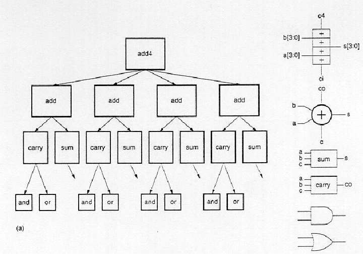
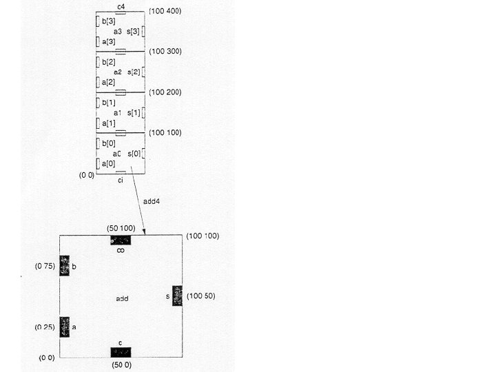
Concepts of Regularity, Modularity and Locality • Regularity means that the hierarchical decomposition of a large system should result in not only simple, but also similar blocks, as much as possible. • Regularity can exist at all levels of abstraction: At the transistor level, uniformly sized transistors simplify the design. At the logic level, identical gate structures can be used, etc. Figure 1. 11 shows regular circuit-level designs of a 2 -1 MUX (multiplexer), an D-type edge-triggered flip flop, and a one-bit full adder.
Figure-1. 11: Regular design of a 2 -1 MUX, a DFF and an adder, using inverters and tri-state buffer
Modularity • Modularity in design means that the various functional blocks which make up the larger system must have welldefined functions and interfaces. • Modularity allows that each block or module can be designed relatively independently from each other, since there is no ambiguity about the function and the signal interface of these blocks. • All of the blocks can be combined with ease at the end of the design process, to form the large system. • The concept of modularity enables the parallelisation of the design process. • It also allows the use of generic modules in various designs - the well-defined functionality and signal interface allow plug-and-play design.
Locality • The concept of locality also ensures that connections are mostly between neighboring modules, avoiding long-distance connections as much as possible. • This last point is extremely important for avoiding excessive interconnect delays. • Time-critical operations should be performed locally, without the need to access distant modules or signals. If necessary, the replication of some logic may solve this problem in large system architectures.
Question Bank 1. Explain VLSI Design flow using Y-chart. OR Explain the VLSI design flow using the D‟Gajski‟s „Y‟ – chart. 2. Answer the following: (I) Compare Semicustom and Full custom VLSI design style (II) Discuss general architecture of FPGA 3. Discuss VLSI Design flow in detail 4. List VLSI design styles and discuss FPGA
Question Bank 5. Discuss following approaches (with examples) used to reduce complexity of IC design: 1. Hierarchy, 2. Regularity, 3. Modularity, and 4. Locality. 6. Discuss following criteria which are considered to measure the quality of chip design. 1. Testability 2. Yield and manufacturability 3. Reliability 4. Technology updateability. OR Which are the four general criteria to measure design quality of a fabricated integrated circuit (chip)? Briefly explain each of them (1. Testability 2. Yield and manufacturability 3. Reliability 4. Technology updateability) 7. Give comparison between FPGA and CPLD.