Mixed Signal VLSI DESIGN Basics of CMOS Analog

“Mixed Signal VLSI DESIGN: Basics of CMOS Analog, Digital and RF Circuits” Arun N. Chandorkar Department of Electrical Engineering Indian Institute of Technology, Bombay Powai, Mumbai-400076, India E-Mail: anc@ee. iitb. ac. in 16 th March 2009

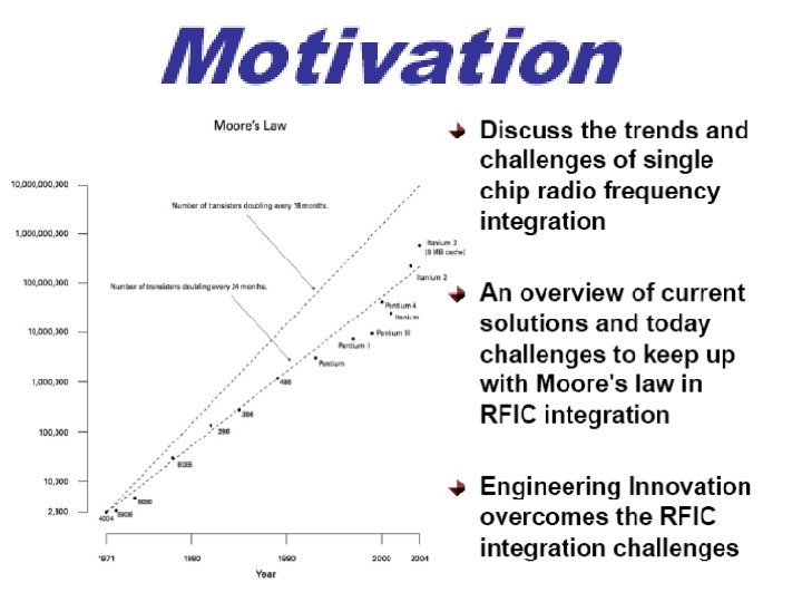
Mixed Signal Basics OUTLINE: • 1. Technology • 2. Analog Design issues • 3. Digital Design Blocks • 4. RF design issues • 5. Components • 6. Conclusion

“Mixed Signal VLSI DESIGN” Basics of CMOS Technology 16 th March 2009

CMOS Process sequence for Mixed Signal Circuits Reference: CMOS Mixed Signal Design : R. J. Baker

CMOS Process sequence for Mixed Signal Circuits Reference: CMOS Mixed Signal Design : R. J. Baker

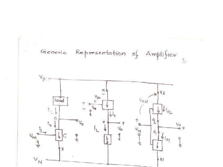
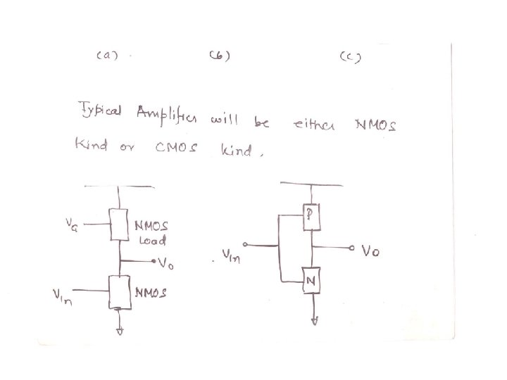
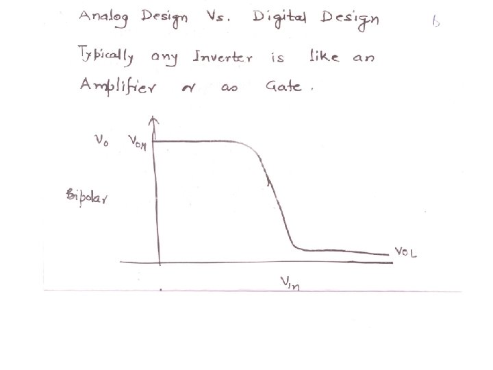
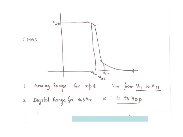
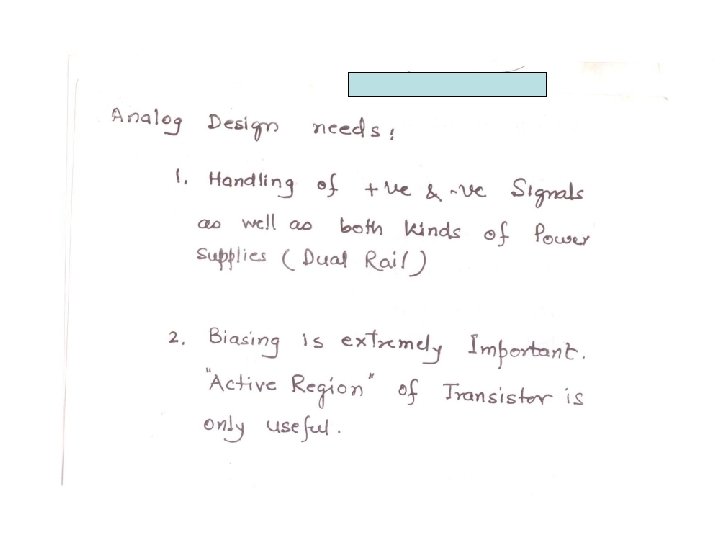
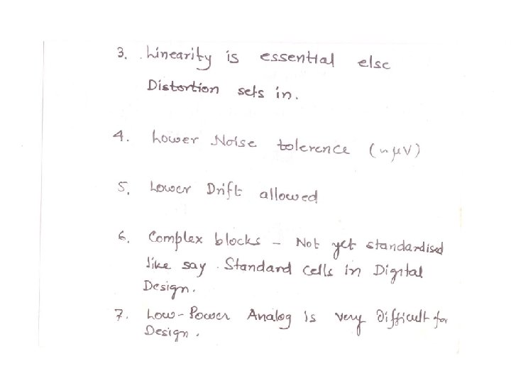
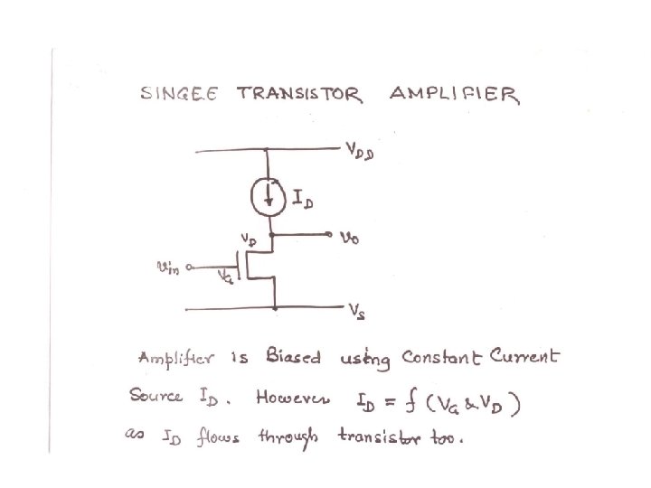
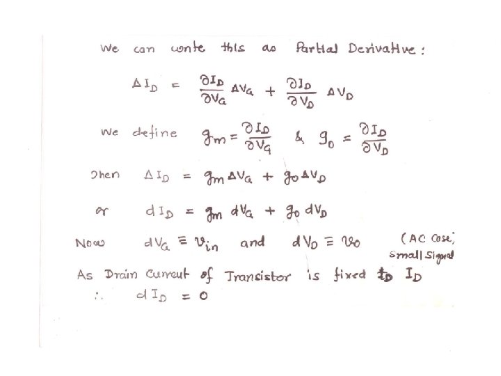
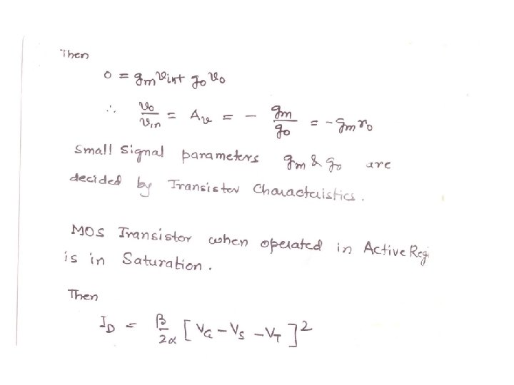
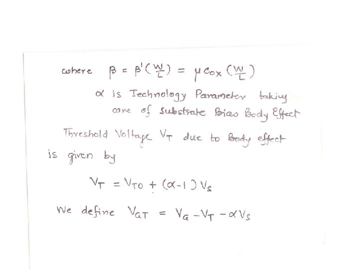
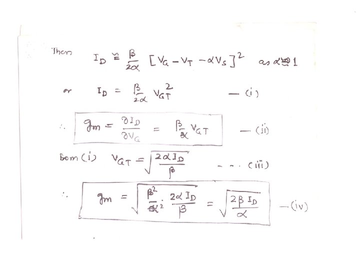
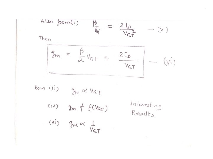
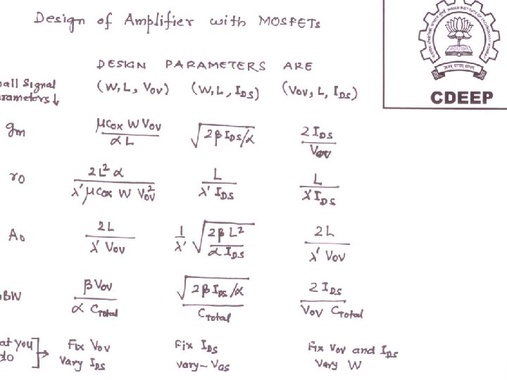
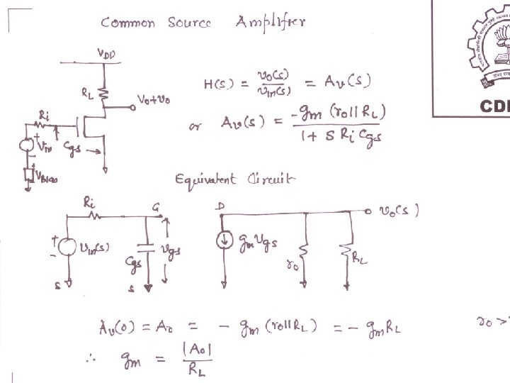
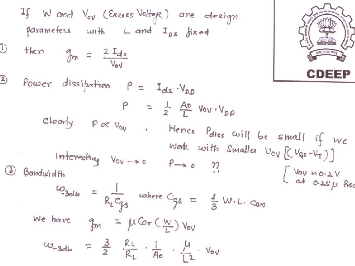
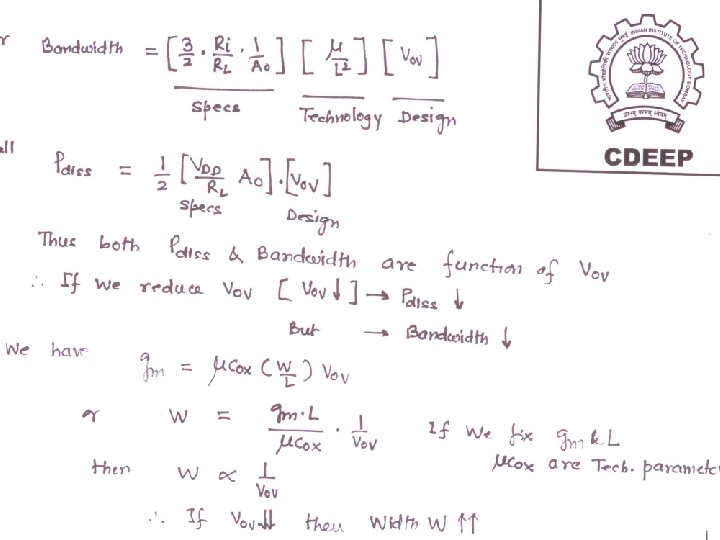
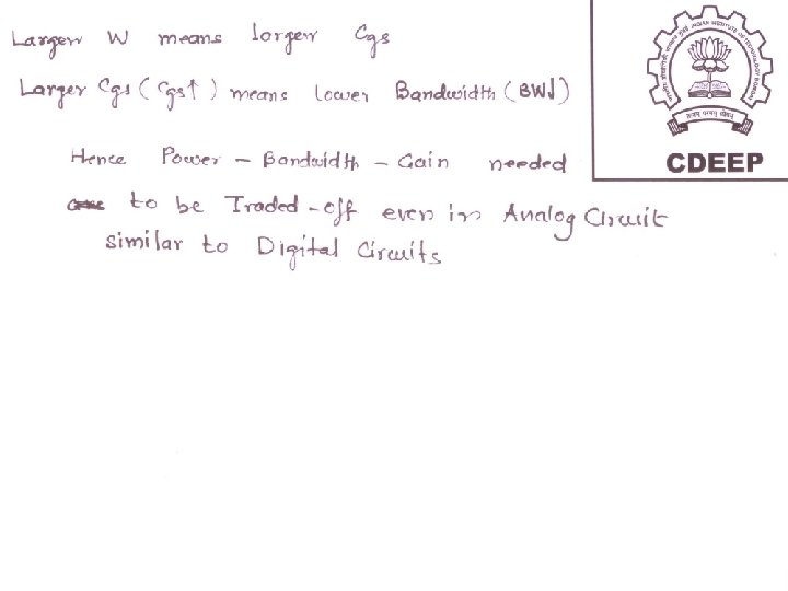
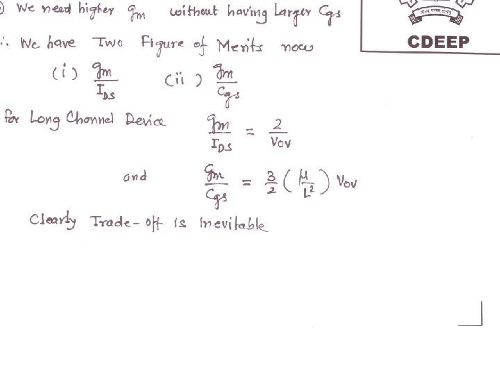
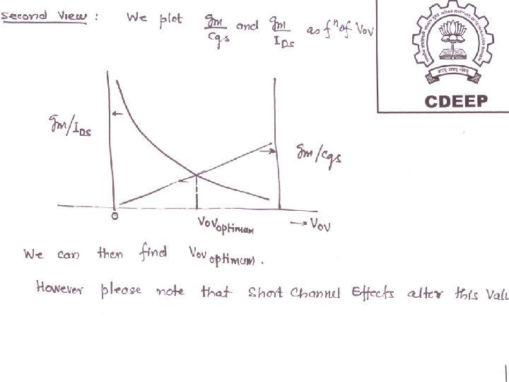
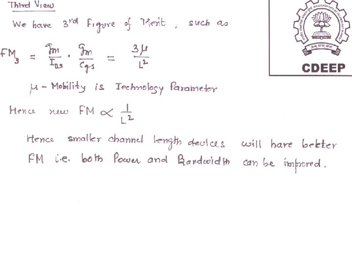
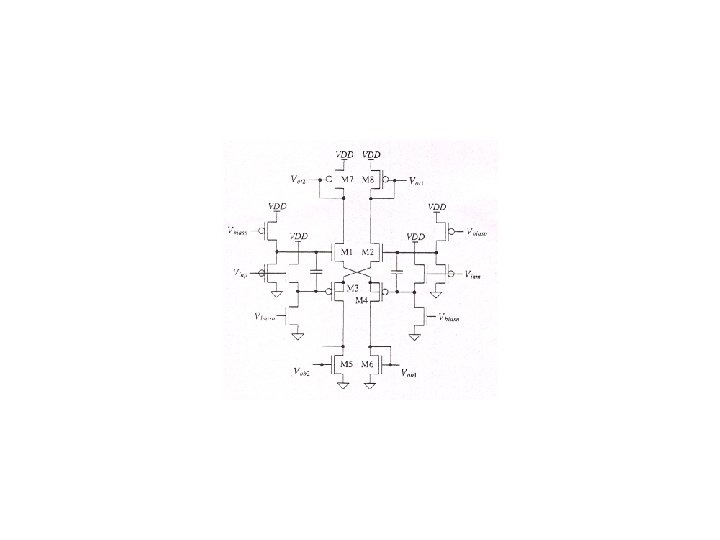
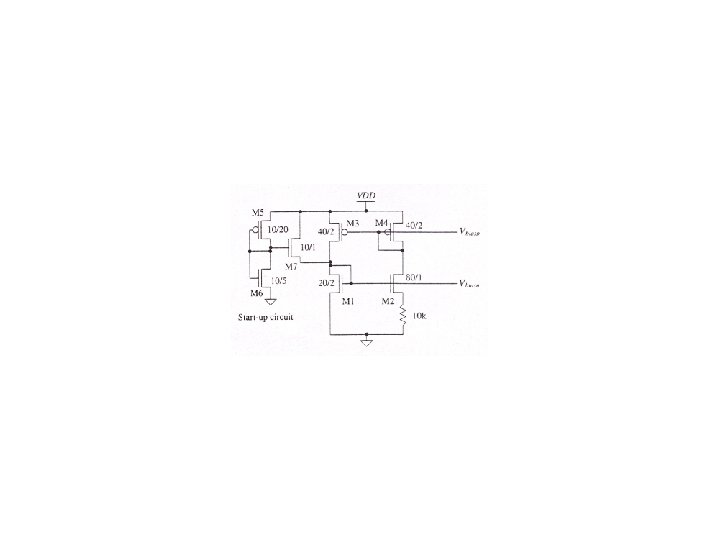
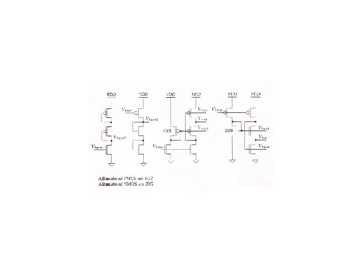
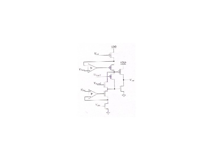
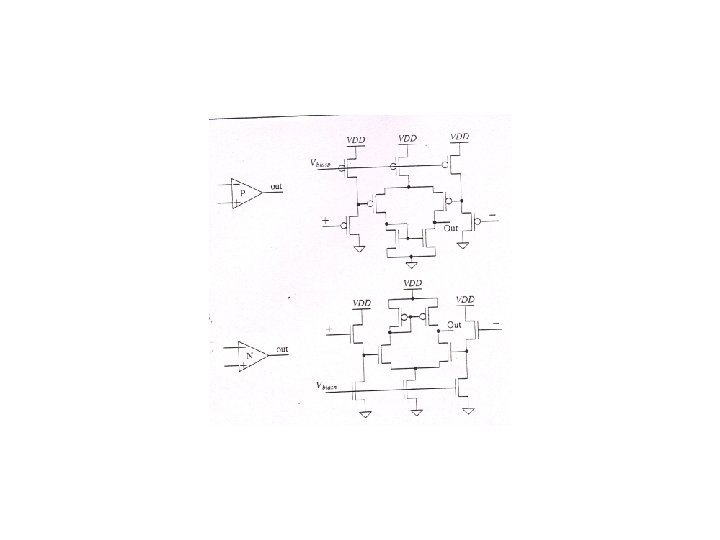
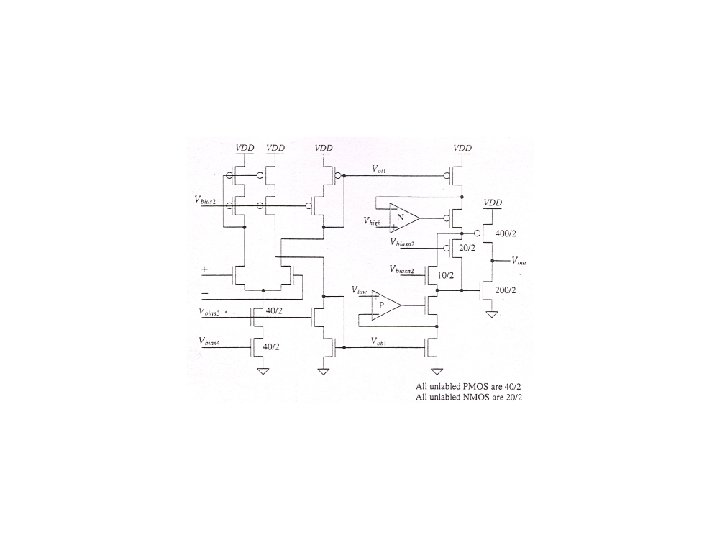
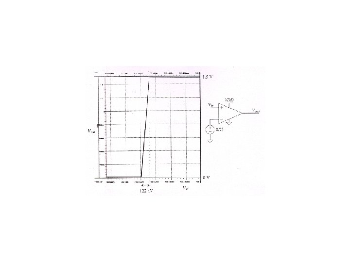
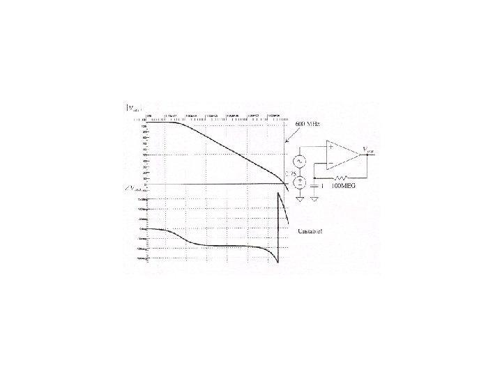
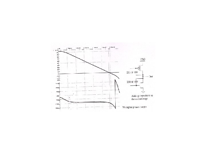
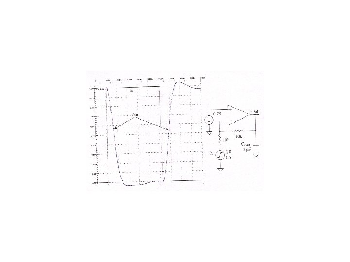
“Mixed Signal VLSI DESIGN” Basics of CMOS Analog Circuits” 16 th March 2009

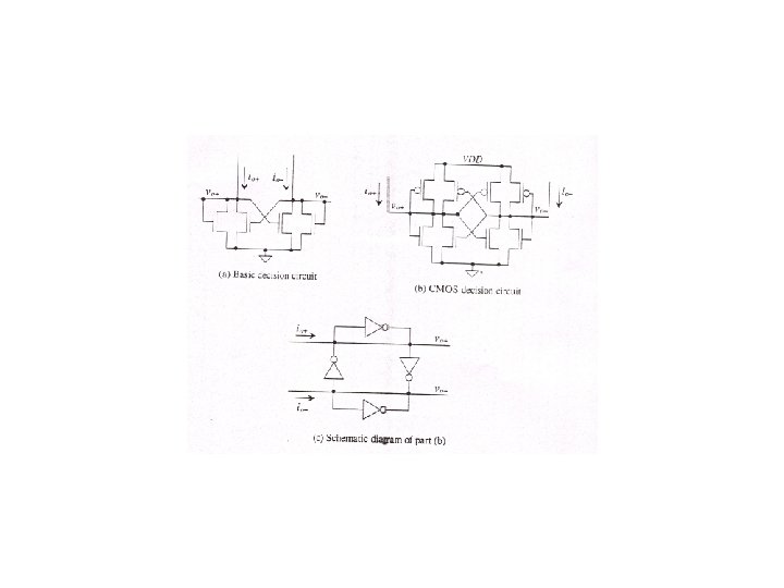
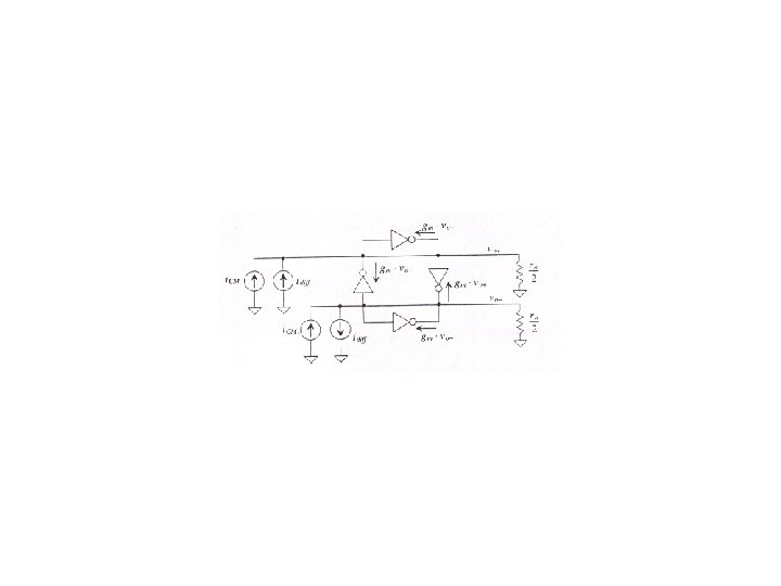
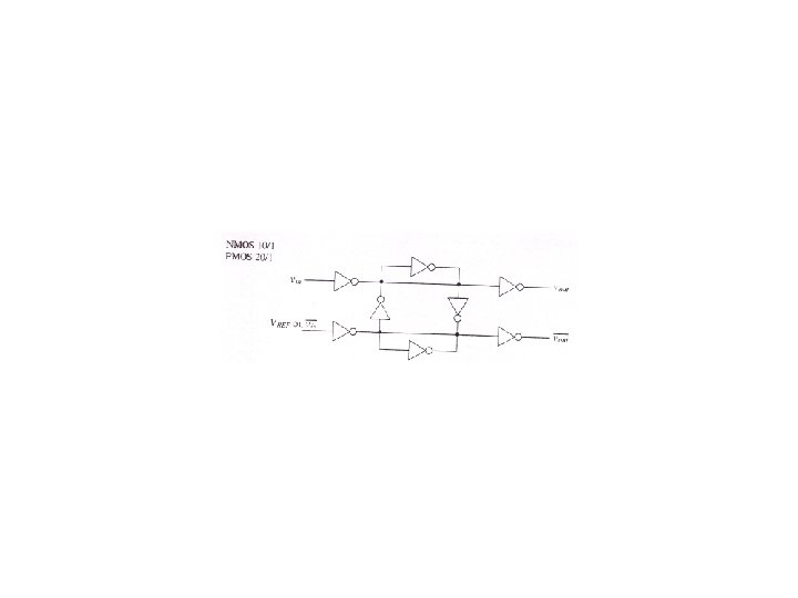
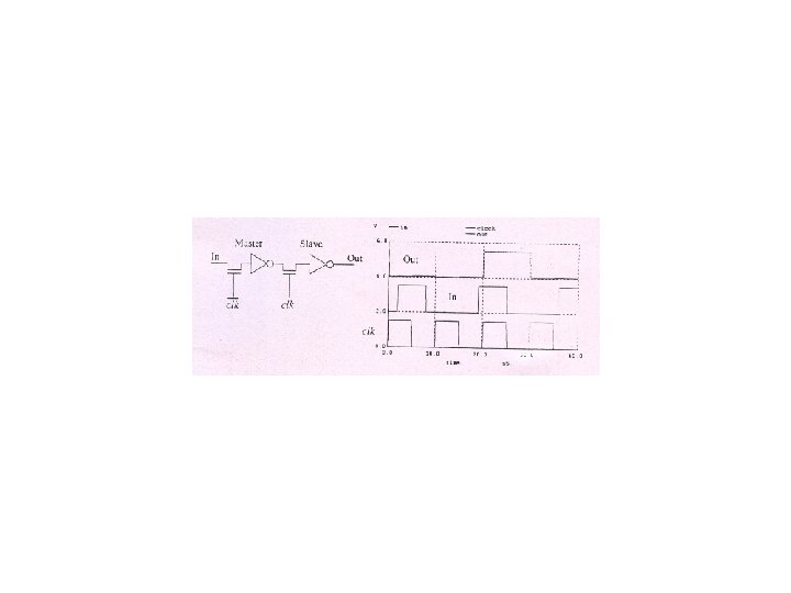
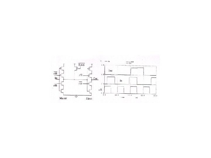
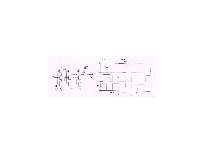
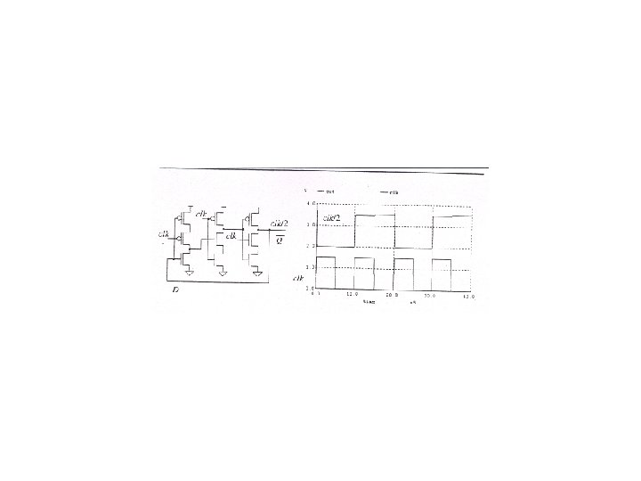
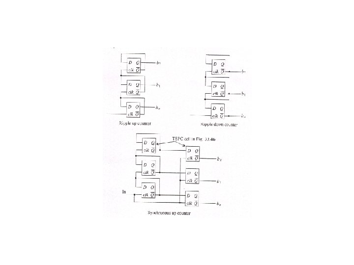
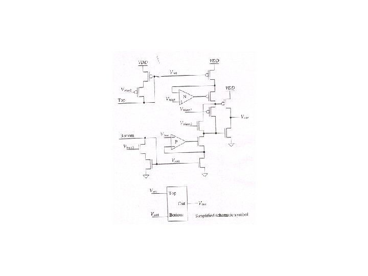
“Mixed Signal VLSI DESIGN: Basics Blocks of CMOS Digital Circuits”

Reference: CMOS Mixed Signal Design : R. J. Baker

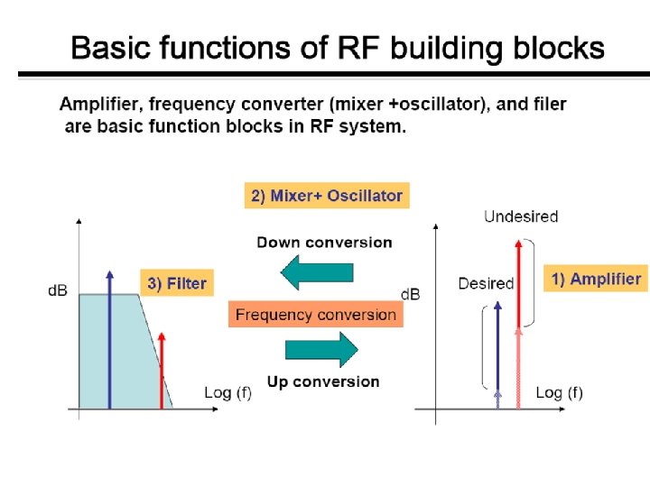
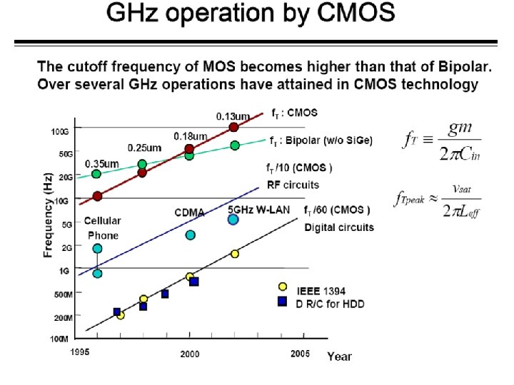
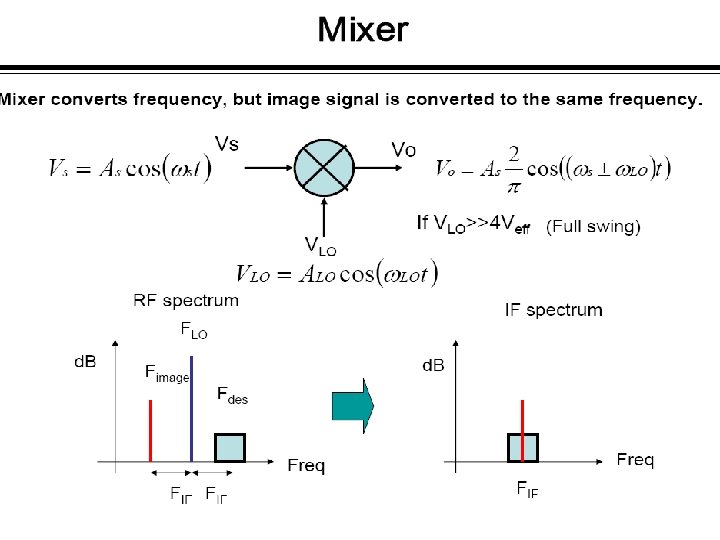
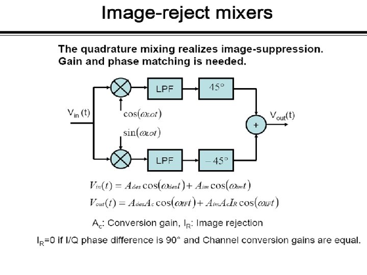
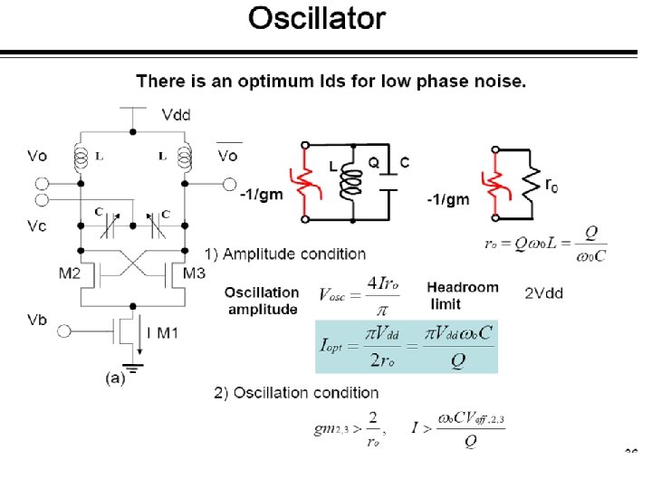
“Mixed Signal VLSI DESIGN” Basics of CMOS RF Circuits 16 th March 2009

RF VLSI Design: Issues and Applications

RF Systems for VLSI Design Global System for Mobile communications (GSM: originally from Groupe Spécial Mobile) is the most popular standard for mobile phones in the world. GSM is a cellular network, which means that mobile phones connect to it by searching for cells in the immediate vicinity. GSM networks operate in four different frequency ranges. Most GSM networks operate in the 900 MHz or 1800 MHz bands. Some countries in the Americas (including Canada and the United States) use the 850 MHz and 1900 MHz bands because the 900 and 1800 MHz frequency bands were already allocated. The rarer 400 and 450 MHz frequency bands are assigned in some countries, notably Scandinavia, where these frequencies were previously used for firstgeneration systems. In the 900 MHz band the uplink frequency band is 890– 915 MHz, and the downlink frequency band is 935– 960 MHz. This 25 MHz bandwidth is subdivided into 124 carrier frequency channels, each spaced 200 k. Hz apart. Time division multiplexing is used to allow eight full-rate or sixteen half-rate speech channels per radio frequency channel. There are eight radio timeslots (giving eight burst periods) grouped into what is called a TDMA frame. Half rate channels use alternate frames in the same timeslot. The channel data rate is 270. 833 kbit/s, and the frame duration is 4. 615 ms.
 Code division multiple access (CDMA) is a channel access method")
RF Systems ( Continued) Code division multiple access (CDMA) is a channel access method utilized by various radio communication technologies. W-CDMA (Wideband Code Division Multiple Access) is a type of 3 G cellular network. W-CDMA is the higher speed transmission protocol used in the UMTS system. Universal Mobile Telecommunications System (UMTS) is one of the thirdgeneration (3 G) cell phone technologies. Currently, the most common form uses W-CDMA. Wi-Fi is a Wireless technology brand owned by the Wi-Fi Alliance intended to improve the interoperability of wireless. Wi. MAX, the Worldwide Interoperability for Microwave Access, is a telecommunications technology aimed at providing wireless data over long distances in a variety of ways, from point-to-point links to full mobile cellular type access. It is based on the IEEE 802. 16 standard, which is also called Wireless. MAN. . A wireless LAN or WLAN is a wireless local area network, which is the linking of two or more computers without using wires. WLAN utilizes spread-spectrum or OFDM modulation technology DCS 1800 - Digital Cellular System 1800 MHz is a term given to what is now known as GSM 1800

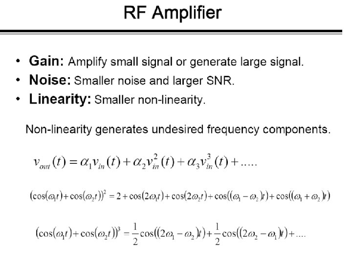
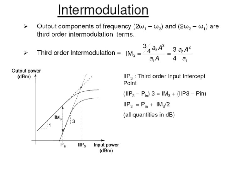
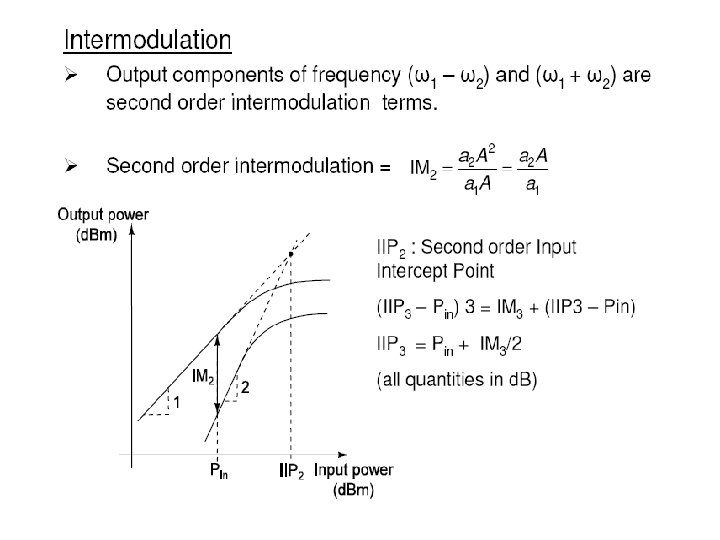
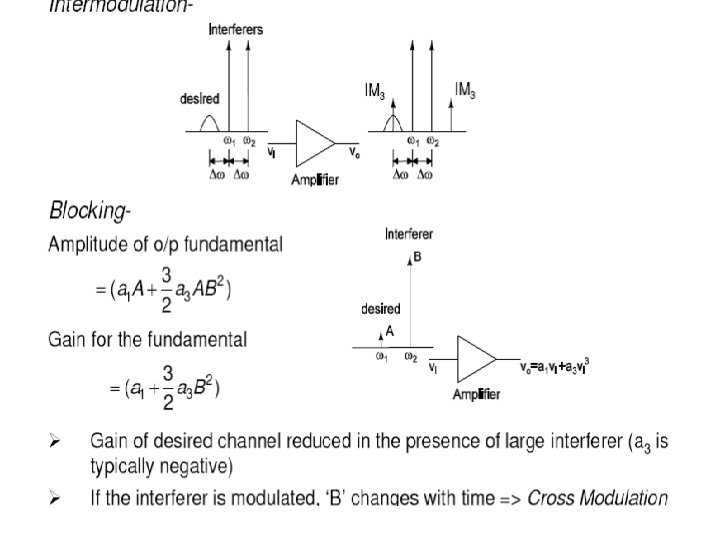
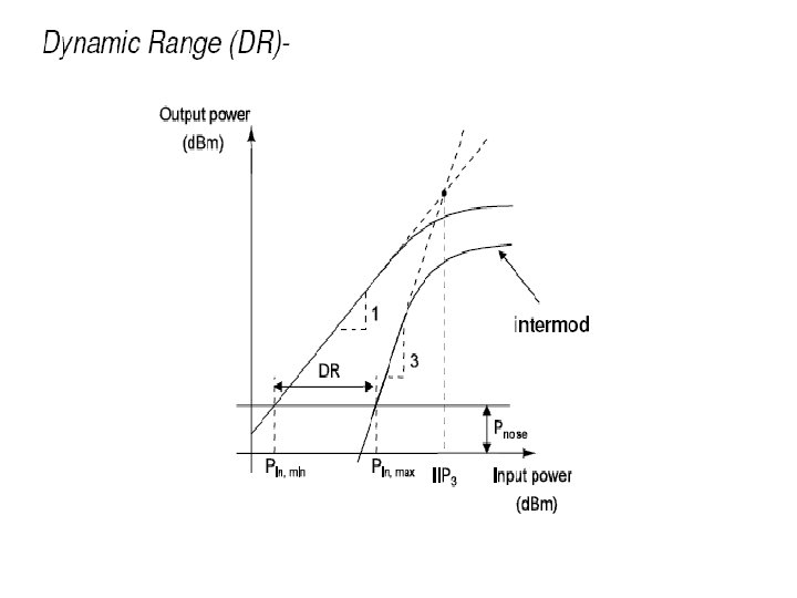
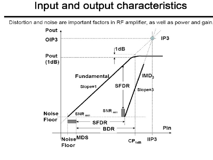
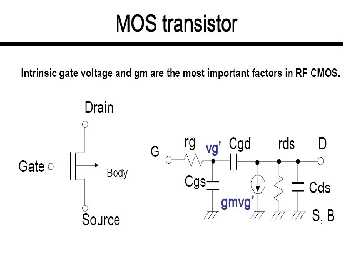
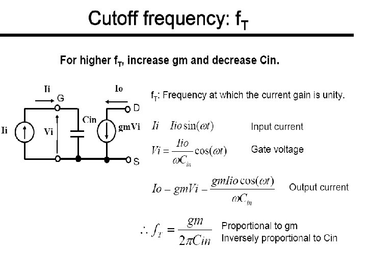
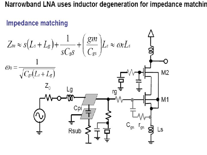
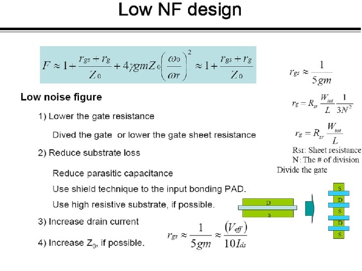
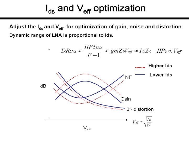
RF Design Issues • • • Linearity Dynamic Range and Power Distortion Noise Impedance matching Modeling of devices at RF frequencies Temperature dependence Modeling of passive components Matching between the components Power consumption High frequency figure of merit, f. T should be at least five times higher than the operating frequency

RF Design Hexagon
")
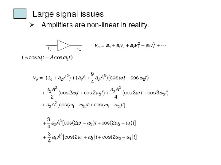
Large Signal Issues ( Cont. )

“Mixed Signal VLSI DESIGN” Basics Circuit Components in CMOS Technology 16 th March 2009

Low Frequency C-V of MOS capacitor Reference: CMOS Mixed Signal Design : R. J. Baker

Floating MOS Capacitor Reference: CMOS Mixed Signal Design : R. J. Baker

Reference: CMOS Mixed Signal Design : R. J. Baker

Reference: CMOS Mixed Signal Design : R. J. Baker

Reference: CMOS Mixed Signal Design : R. J. Baker

Resistors Realization in CMOS Technology

Spiral Segment of Inductor on Si

Inductors in MOS Technology • The self-inductance for a straight conductor is L = 0. 0021[ ln { 2 l /GMD} -1. 25 + (AMD/l) + (m/4) T ] Where L is the self-inductance in micro henries, l is the conductor length in cm, GMD and AMD represent the geometric and arithmetic mean distance, respectively, of the conductor cross section, m is the conductor permeability, and T is the frequency correction parameter. • The geometric mean distance (GMD) between two conductors is the distance between two infinitely thin imaginary filaments whose mutual inductance is equal to the mutual inductance between the two original conductors. The GMD is equal to 0. 44705 times a side in the case of a square cross section. • The arithmetic mean distance (AMD) is the average of all the distances between the points of one conductor and the points of another. For a single conductor, the arithmetic mean distance is the average of all possible distances within the cross section.

Variation in Frequency-Correction Parameter T Table. 1 Thin Value of T Films and Microwave Frequencies. Film Thickness Frequency 0. 9974 10000 A 10 gigahertz 0. 9986 0. 9095 0. 0025 mm 1 gigahertz 0. 0075 mm 1 gigahertz
 + sqrt {1+")
Inductance of spiral • M = 2 l Q where Q=ln[(1/GMD) + sqrt {1+ (l 2 / GMD 2)}] – sqrt { 1+ (GMD 2 / l 2) } + (GMD/l) • Total Inductance is then given by: L T = L 0 + M + + M – where L 0 is the sum of the self-inductances of all straight segments, M + is the sum of the positive mutual inductances and M – is the sum of th negative mutual inductances

Spiral Inductor

Physical Inductor Model
 which means the inductance of the")
Mutual inductance Zin = j w w (L+M) which means the inductance of the conductor increases by M, and M is the mutual inductance between the two conductors. So, parallel currents traveling in phase’ can contribute positive mutual components of inductance. Thus the inductance of a conductor can be expressed as, L = Lself ± M M=2 l. Q where Q=ln[(1/GMD) + sqrt {1+ (l 2 / GMD 2)}] – sqrt { 1+ (GMD 2 / l 2 } + (GMD/l) LT = L 0 + M + + M -

Layout of Spiral inductor and probe pads for measurement.

RF inductor issues

Acknowledgements TO My Graduate students of last 10 Years, Who did their Projects With me in Analog, Digital and RF Designs & Also those who participated in my courses in “Digital VLSI Design”, “Analog VLSI Design” VLSI technology, RF VLSI and System Design. Thanks to authors who put their work on Many Websites and they are as referred in the PPTs

Thank-you
- Slides: 101