
Introduction to VLSI Design l l l Instructor



- Slides: 32
Introduction to VLSI Design l l l Instructor: Steven P. Levitan levitan@ee. pitt. edu TA: Jeremiah Cessna jecst 40@pitt. edu Book: Digital Integrated Circuits: A Design Perspective; Jan Rabaey Lab Notes: at Copycat http: //kona. ee. pitt. edu/steve/EE 1192 http: //infopad. EECS. Berkeley. EDU/~icdesign/ Introduction to VLSI Design Introduction © Steven P. Levitan 1998
Digital Integrated Circuits A Design Perspective Jan M. Rabaey
Course Outline (approximate) – Introduction and Motivation – The VLSI Design Process – Details of the MOS Transistor – Device Fabrication – Design Rules – CMOS circuits – VLSI Structures – System Timing – Real Circuits and Performance Introduction to VLSI Design Introduction © Steven P. Levitan 1998
Reference Books – Principles of CMOS VLSI Design: Neil Weste and Kamran Eshraghian – CMOS: Baker, Li, Boyce – Application Specific Integrated Circuits: Smith – The Design and Analysis of VLSI – Circuits: Lance Glasser and Daniel Dobberpuhl – Introduction to VLSI Systems: Carver Mead & Lynn Conway – News. Groups: comp. lsi, comp. lsi. cad Introduction to VLSI Design Introduction © Steven P. Levitan 1998
Software – Magic l l Unix Based Interactive Design Rule Checking Circuit Extraction Supported Technology files – Spice l l Well known and disliked Spice 3 allows user models Good support/documentation Interface with Magic extraction – Irsim l l l Switch / Switched - Resistor level Fast functional validation Good interface with Magic Introduction to VLSI Design Introduction © Steven P. Levitan 1998
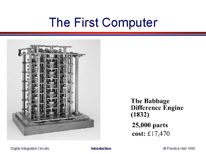
The First Computer Digital Integrated Circuits Introduction © Prentice Hall 1995
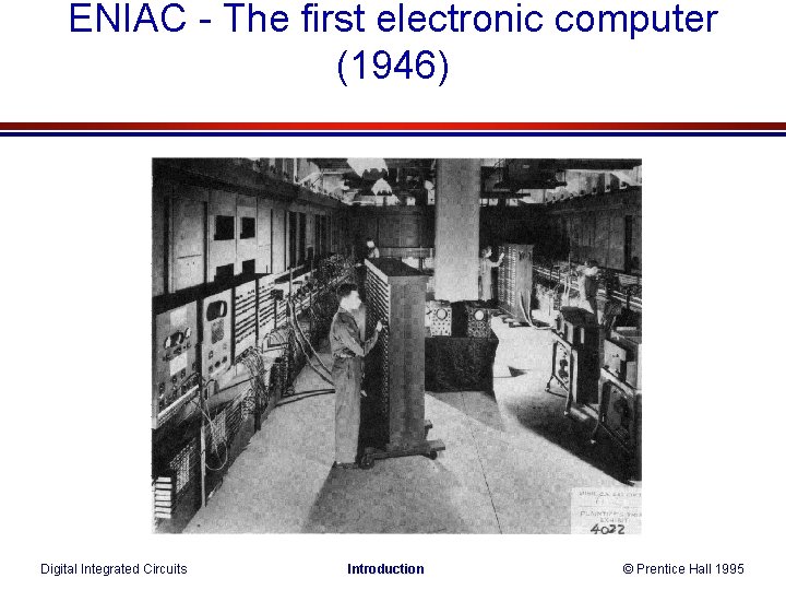
ENIAC - The first electronic computer (1946) Digital Integrated Circuits Introduction © Prentice Hall 1995
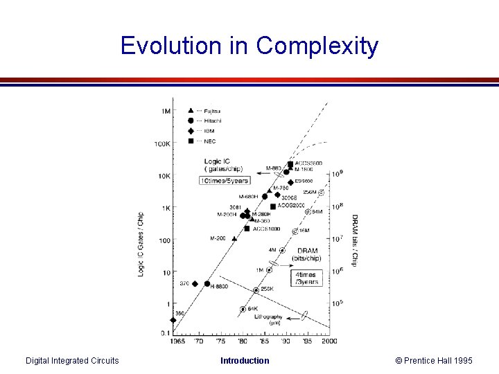
Evolution in Complexity Digital Integrated Circuits Introduction © Prentice Hall 1995
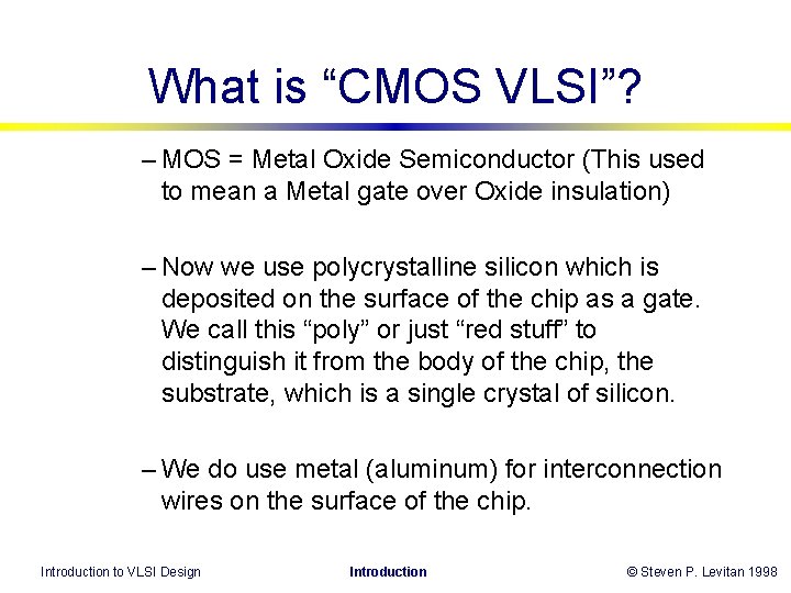
What is “CMOS VLSI”? – MOS = Metal Oxide Semiconductor (This used to mean a Metal gate over Oxide insulation) – Now we use polycrystalline silicon which is deposited on the surface of the chip as a gate. We call this “poly” or just “red stuff” to distinguish it from the body of the chip, the substrate, which is a single crystal of silicon. – We do use metal (aluminum) for interconnection wires on the surface of the chip. Introduction to VLSI Design Introduction © Steven P. Levitan 1998
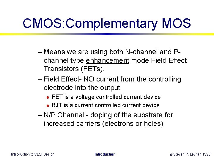
CMOS: Complementary MOS – Means we are using both N-channel and Pchannel type enhancement mode Field Effect Transistors (FETs). – Field Effect- NO current from the controlling electrode into the output l l FET is a voltage controlled current device BJT is a current controlled current device – N/P Channel - doping of the substrate for increased carriers (electrons or holes) Introduction to VLSI Design Introduction © Steven P. Levitan 1998
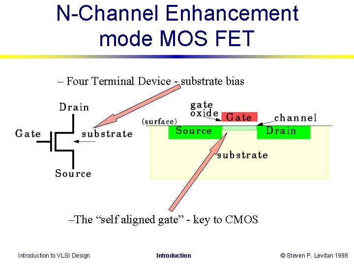
N-Channel Enhancement mode MOS FET – Four Terminal Device - substrate bias –The “self aligned gate” - key to CMOS Introduction to VLSI Design Introduction © Steven P. Levitan 1998
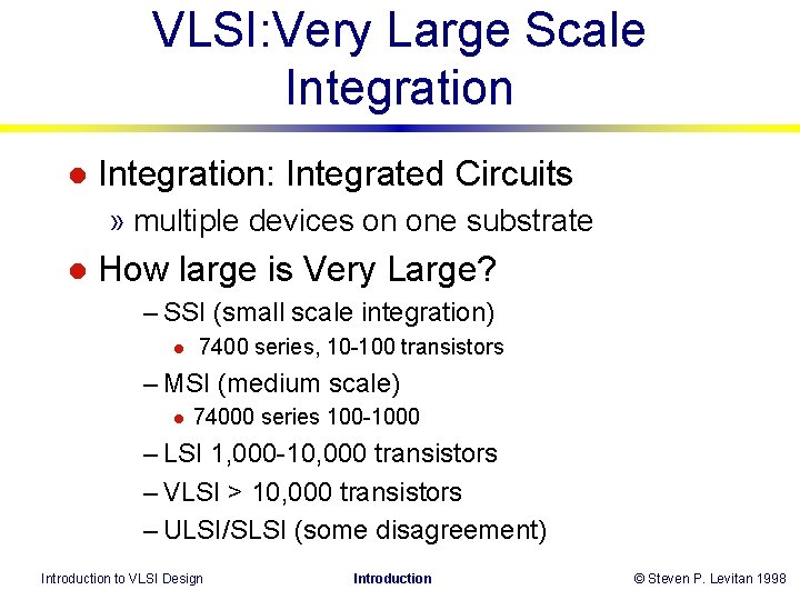
VLSI: Very Large Scale Integration l Integration: Integrated Circuits » multiple devices on one substrate l How large is Very Large? – SSI (small scale integration) l 7400 series, 10 -100 transistors – MSI (medium scale) l 74000 series 100 -1000 – LSI 1, 000 -10, 000 transistors – VLSI > 10, 000 transistors – ULSI/SLSI (some disagreement) Introduction to VLSI Design Introduction © Steven P. Levitan 1998
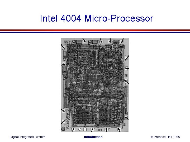
Intel 4004 Micro-Processor Digital Integrated Circuits Introduction © Prentice Hall 1995
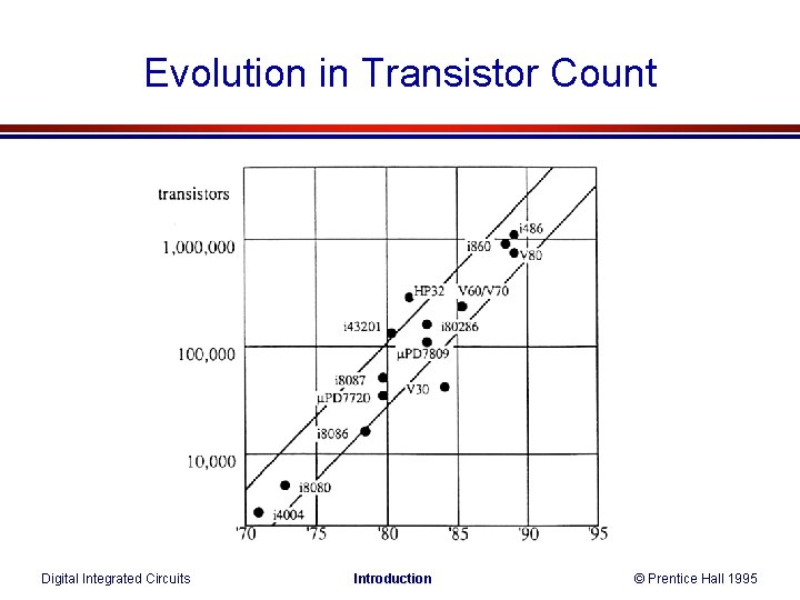
Evolution in Transistor Count Digital Integrated Circuits Introduction © Prentice Hall 1995
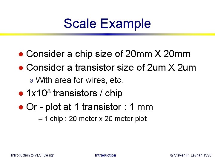
Scale Example Consider a chip size of 20 mm X 20 mm l Consider a transistor size of 2 um X 2 um l » With area for wires, etc. 1 x 10⁸ transistors / chip l Or - plot at 1 transistor : 1 mm l – 1 chip : 20 meter x 20 meter plot Introduction to VLSI Design Introduction © Steven P. Levitan 1998
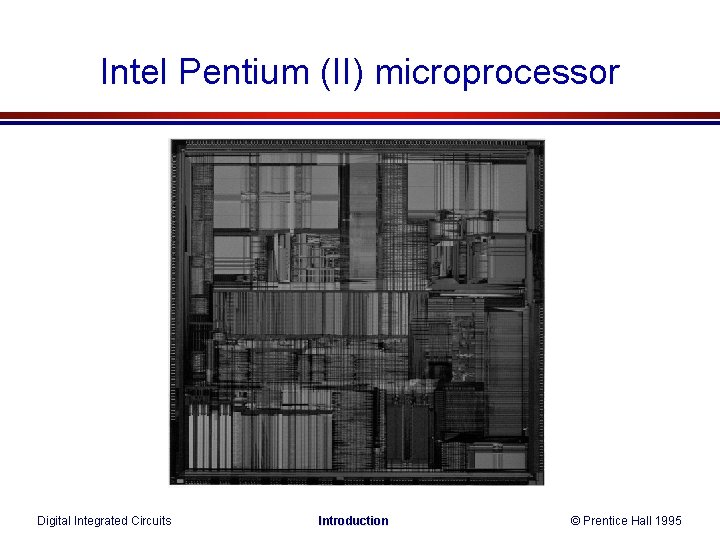
Intel Pentium (II) microprocessor Digital Integrated Circuits Introduction © Prentice Hall 1995
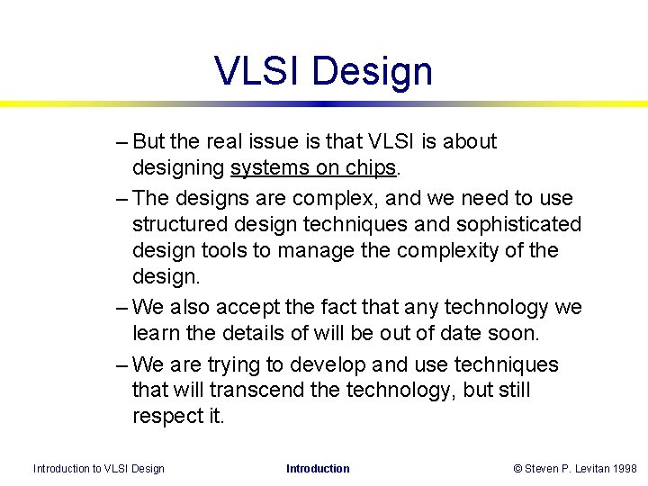
VLSI Design – But the real issue is that VLSI is about designing systems on chips. – The designs are complex, and we need to use structured design techniques and sophisticated design tools to manage the complexity of the design. – We also accept the fact that any technology we learn the details of will be out of date soon. – We are trying to develop and use techniques that will transcend the technology, but still respect it. Introduction to VLSI Design Introduction © Steven P. Levitan 1998
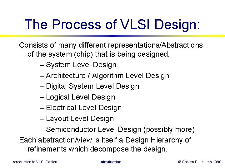
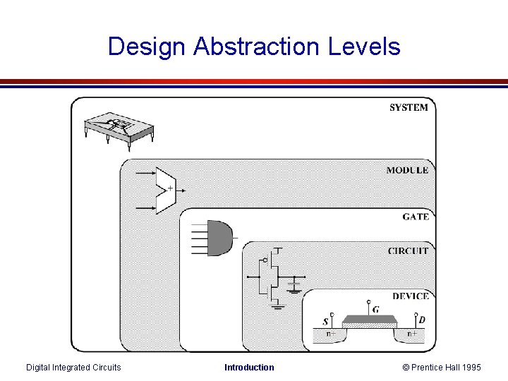
The Process of VLSI Design: Consists of many different representations/Abstractions of the system (chip) that is being designed. – System Level Design – Architecture / Algorithm Level Design – Digital System Level Design – Logical Level Design – Electrical Level Design – Layout Level Design – Semiconductor Level Design (possibly more) Each abstraction/view is itself a Design Hierarchy of refinements which decompose the design. Introduction to VLSI Design Introduction © Steven P. Levitan 1998
Design Abstraction Levels Digital Integrated Circuits Introduction © Prentice Hall 1995
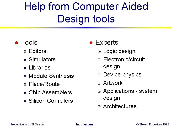
Help from Computer Aided Design tools l Tools » » » » l » Logic design » Electronic/circuit design » Device physics » Artwork » Applications - system design » Architectures Editors Simulators Libraries Module Synthesis Place/Route Chip Assemblers Silicon Compilers Introduction to VLSI Design Experts Introduction © Steven P. Levitan 1998
New Design Methodologies l Methodologies which are based on: » System Level Abstractions v. s. Device Characteristic Abstractions – Logic structures and circuitry change slowly over time l trade-offs do change, but the choices do not » Scalable Designs – Layout techniques also change slowly. l But the minimum feature size steadily decreases with time (also Voltage, Die Size, etc. ) Introduction to VLSI Design Introduction © Steven P. Levitan 1998
Design Approaches – Custom l l full control of design best results, slowest design time. – Semi-custom (std cell) l l use Cell libraries from vendor cad tools, faster design time – Gate Array l l l fastest design time worst speed/power/density best low volume (worst high volume) – EPLA/EPLD - FPGA - electrically programmable (in the field) Introduction to VLSI Design Introduction © Steven P. Levitan 1998
Close up of Intel Chip? Time Magazine, July 1998 Introduction to VLSI Design Introduction © Steven P. Levitan 1998
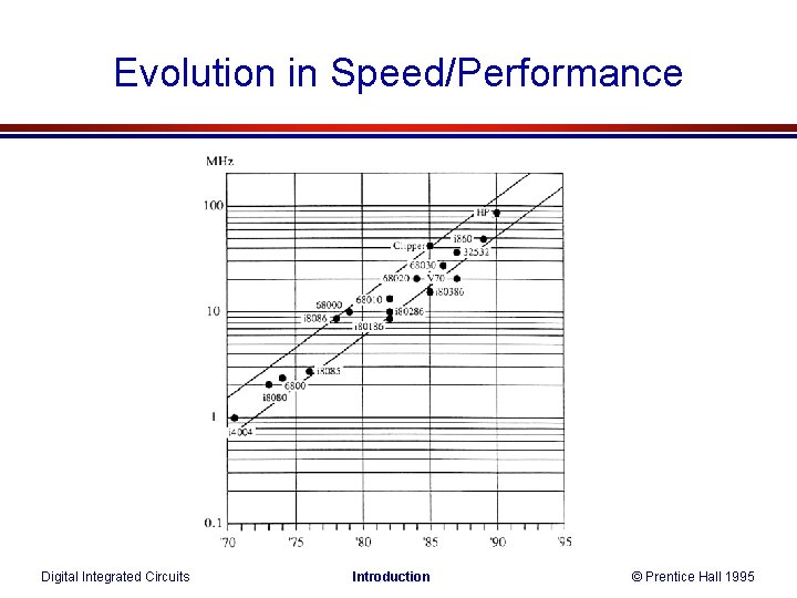
Evolution in Speed/Performance Digital Integrated Circuits Introduction © Prentice Hall 1995
Technologies – Bipolar (BJT) l l l TTL, Schottky ECL I^2 L – Dual Junction, current controlled devices l MOS (FET unipolar) » NMOS, PMOS » CMOS <== our course – Single Junction voltage controlled devices l l Ga. As (typically JFET’s) OEIC’s - MQW’s, Integrated Lasers, ? Introduction to VLSI Design Introduction © Steven P. Levitan 1998
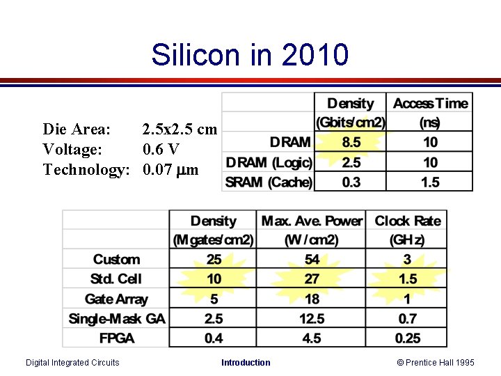
Silicon in 2010 Die Area: 2. 5 x 2. 5 cm Voltage: 0. 6 V Technology: 0. 07 m Digital Integrated Circuits Introduction © Prentice Hall 1995
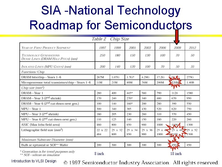
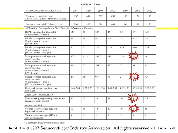
SIA -National Technology Roadmap for Semiconductors Introduction to VLSI Design Introduction © Steven P. Levitan 1998
SIA -National Technology Roadmap for Semiconductors 8 inch Introduction to VLSI Design Introduction 18 inch © Steven P. Levitan 1998
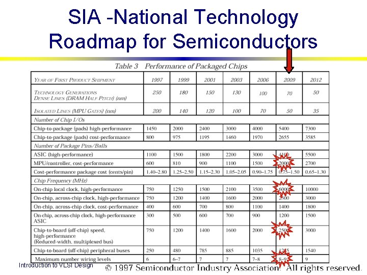
SIA -National Technology Roadmap for Semiconductors Introduction to VLSI Design Introduction © Steven P. Levitan 1998
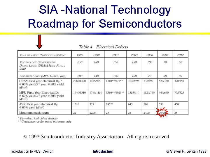
SIA -National Technology Roadmap for Semiconductors Introduction to VLSI Design Introduction © Steven P. Levitan 1998
SIA -National Technology Roadmap for Semiconductors Introduction to VLSI Design Introduction © Steven P. Levitan 1998
SIA -National Technology Roadmap for Semiconductors Introduction to VLSI Design Introduction © Steven P. Levitan 1998