Introduction to CMOS VLSI Design CAMs ROMs and
- Slides: 30

Introduction to CMOS VLSI Design CAMs, ROMs, and PLAs CAMS, ROMs and PLAs 1

Outline q Content-Addressable Memories q Read-Only Memories q Programmable Logic Arrays CAMS, ROMs and PLAs CMOS VLSI Design 2

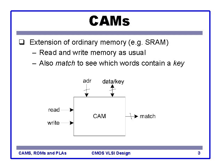
CAMs q Extension of ordinary memory (e. g. SRAM) – Read and write memory as usual – Also match to see which words contain a key CAMS, ROMs and PLAs CMOS VLSI Design 3

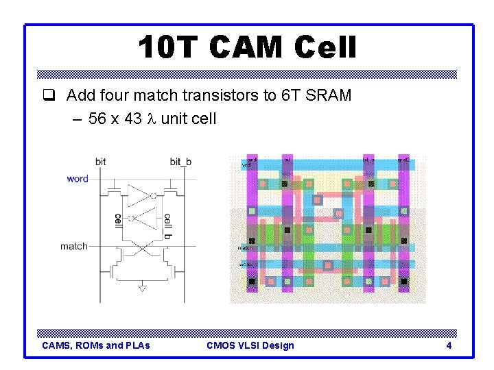
10 T CAM Cell q Add four match transistors to 6 T SRAM – 56 x 43 l unit cell CAMS, ROMs and PLAs CMOS VLSI Design 4

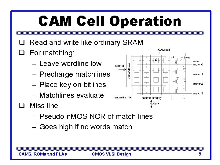
CAM Cell Operation q Read and write like ordinary SRAM q For matching: – Leave wordline low – Precharge matchlines – Place key on bitlines – Matchlines evaluate q Miss line – Pseudo-n. MOS NOR of match lines – Goes high if no words match CAMS, ROMs and PLAs CMOS VLSI Design 5

Read-Only Memories q Read-Only Memories are nonvolatile – Retain their contents when power is removed q Mask-programmed ROMs use one transistor per bit – Presence or absence determines 1 or 0 CAMS, ROMs and PLAs CMOS VLSI Design 6

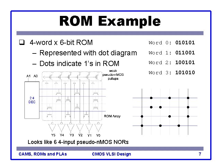
ROM Example q 4 -word x 6 -bit ROM – Represented with dot diagram – Dots indicate 1’s in ROM Word 0: 010101 Word 1: 011001 Word 2: 100101 Word 3: 101010 Looks like 6 4 -input pseudo-n. MOS NORs CAMS, ROMs and PLAs CMOS VLSI Design 7

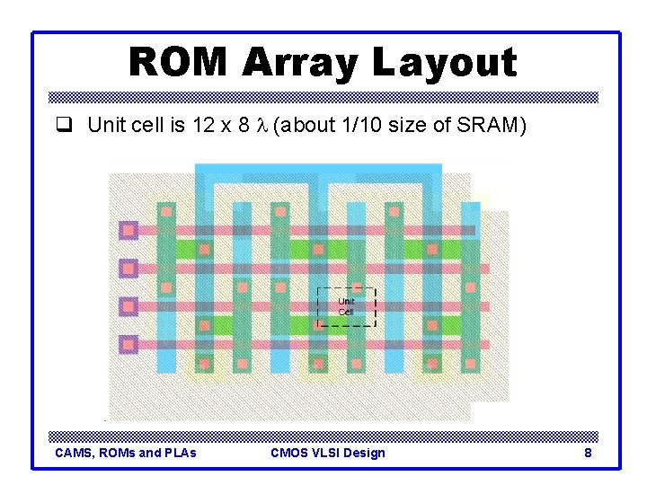
ROM Array Layout q Unit cell is 12 x 8 l (about 1/10 size of SRAM) CAMS, ROMs and PLAs CMOS VLSI Design 8

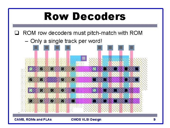
Row Decoders q ROM row decoders must pitch-match with ROM – Only a single track per word! CAMS, ROMs and PLAs CMOS VLSI Design 9

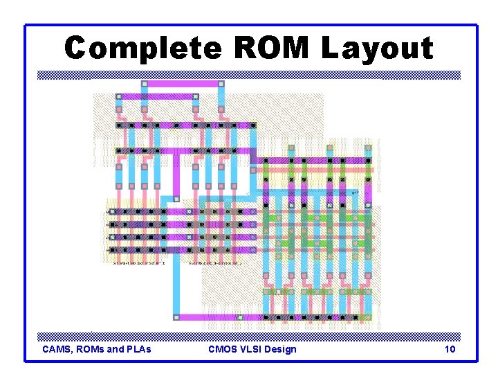
Complete ROM Layout CAMS, ROMs and PLAs CMOS VLSI Design 10

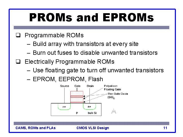
PROMs and EPROMs q Programmable ROMs – Build array with transistors at every site – Burn out fuses to disable unwanted transistors q Electrically Programmable ROMs – Use floating gate to turn off unwanted transistors – EPROM, EEPROM, Flash CAMS, ROMs and PLAs CMOS VLSI Design 11

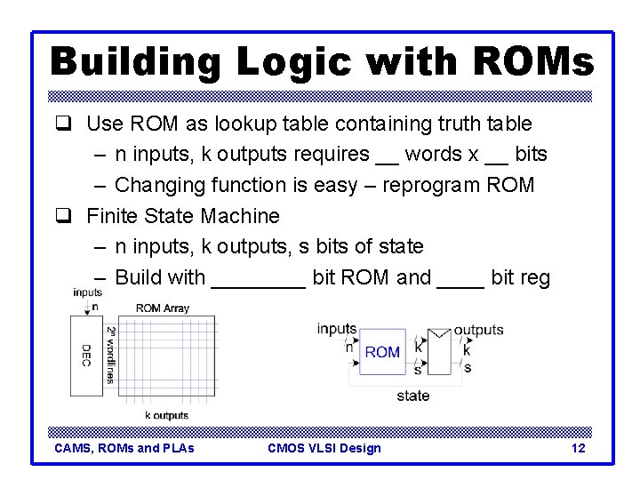
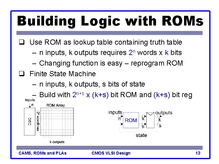
Building Logic with ROMs q Use ROM as lookup table containing truth table – n inputs, k outputs requires __ words x __ bits – Changing function is easy – reprogram ROM q Finite State Machine – n inputs, k outputs, s bits of state – Build with ____ bit ROM and ____ bit reg CAMS, ROMs and PLAs CMOS VLSI Design 12

Building Logic with ROMs q Use ROM as lookup table containing truth table – n inputs, k outputs requires 2 n words x k bits – Changing function is easy – reprogram ROM q Finite State Machine – n inputs, k outputs, s bits of state – Build with 2 n+s x (k+s) bit ROM and (k+s) bit reg CAMS, ROMs and PLAs CMOS VLSI Design 13

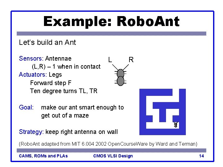
Example: Robo. Ant Let’s build an Ant Sensors: Antennae (L, R) – 1 when in contact Actuators: Legs Forward step F Ten degree turns TL, TR Goal: L R make our ant smart enough to get out of a maze Strategy: keep right antenna on wall (Robo. Ant adapted from MIT 6. 004 2002 Open. Course. Ware by Ward and Terman) CAMS, ROMs and PLAs CMOS VLSI Design 14

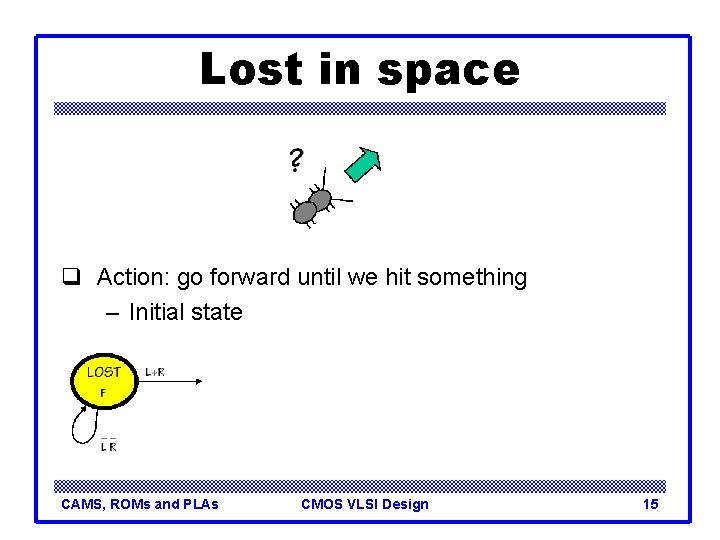
Lost in space q Action: go forward until we hit something – Initial state CAMS, ROMs and PLAs CMOS VLSI Design 15

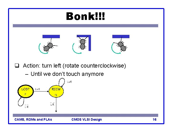
Bonk!!! q Action: turn left (rotate counterclockwise) – Until we don’t touch anymore CAMS, ROMs and PLAs CMOS VLSI Design 16

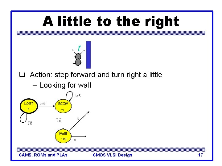
A little to the right q Action: step forward and turn right a little – Looking for wall CAMS, ROMs and PLAs CMOS VLSI Design 17

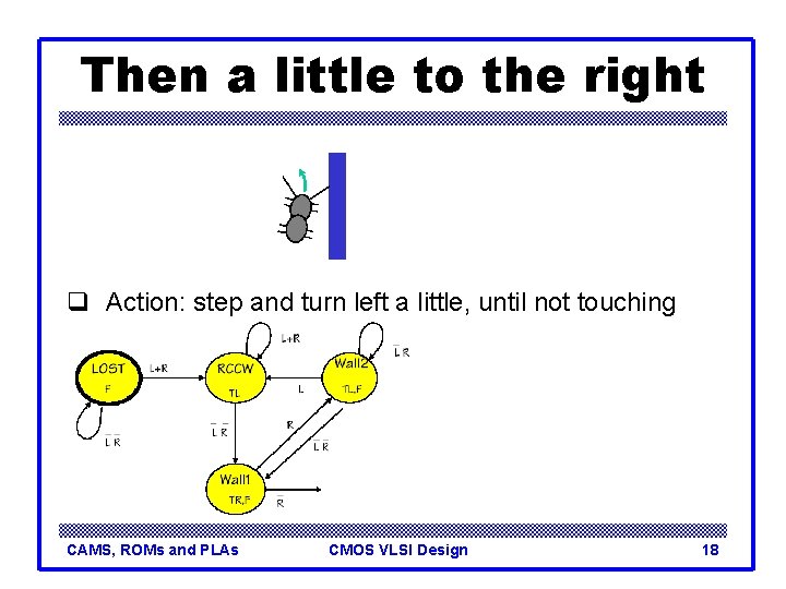
Then a little to the right q Action: step and turn left a little, until not touching CAMS, ROMs and PLAs CMOS VLSI Design 18

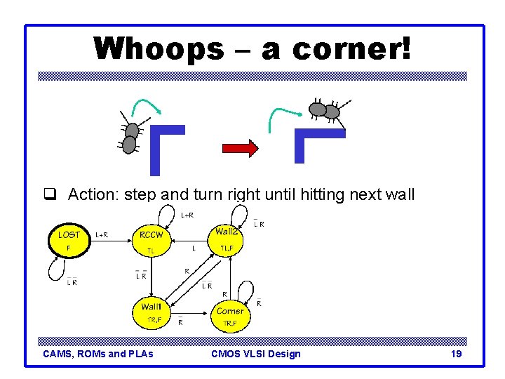
Whoops – a corner! q Action: step and turn right until hitting next wall CAMS, ROMs and PLAs CMOS VLSI Design 19

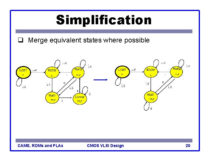
Simplification q Merge equivalent states where possible CAMS, ROMs and PLAs CMOS VLSI Design 20

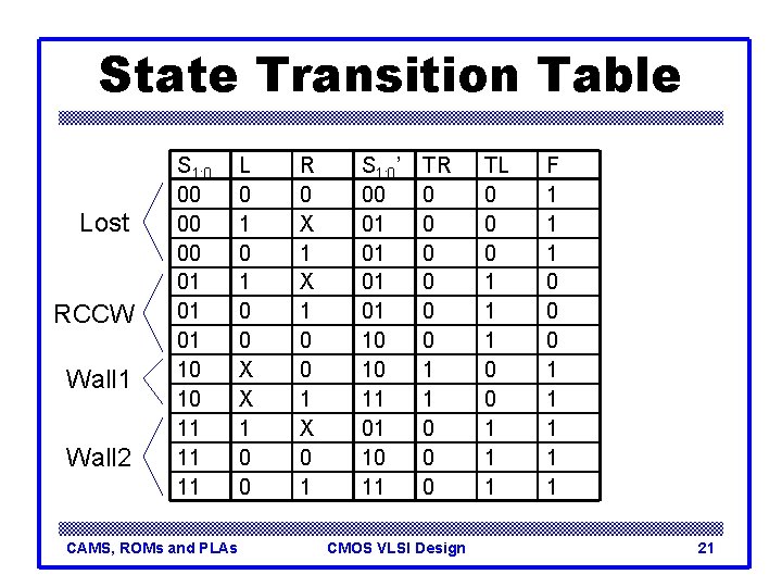
State Transition Table Lost RCCW Wall 1 Wall 2 S 1: 0 00 01 01 01 10 10 11 11 11 CAMS, ROMs and PLAs L 0 1 0 0 X X 1 0 0 R 0 X 1 0 0 1 X 0 1 S 1: 0’ 00 01 01 10 10 11 01 10 11 TR 0 0 0 1 1 0 0 0 CMOS VLSI Design TL 0 0 0 1 1 1 F 1 1 1 0 0 0 1 1 1 21

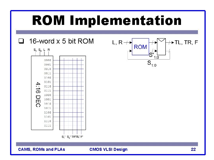
ROM Implementation q 16 -word x 5 bit ROM CAMS, ROMs and PLAs CMOS VLSI Design 22

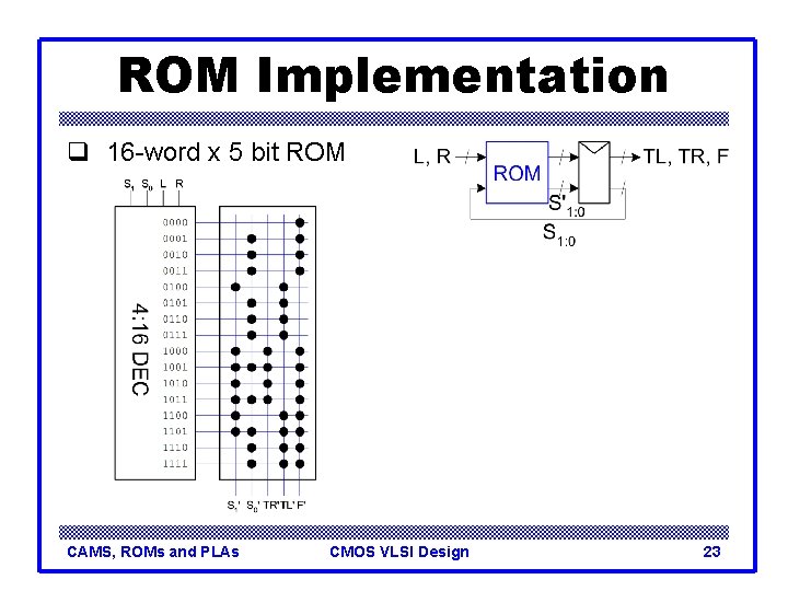
ROM Implementation q 16 -word x 5 bit ROM CAMS, ROMs and PLAs CMOS VLSI Design 23

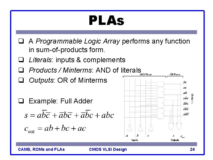
PLAs q A Programmable Logic Array performs any function in sum-of-products form. q Literals: inputs & complements q Products / Minterms: AND of literals q Outputs: OR of Minterms q Example: Full Adder CAMS, ROMs and PLAs CMOS VLSI Design 24

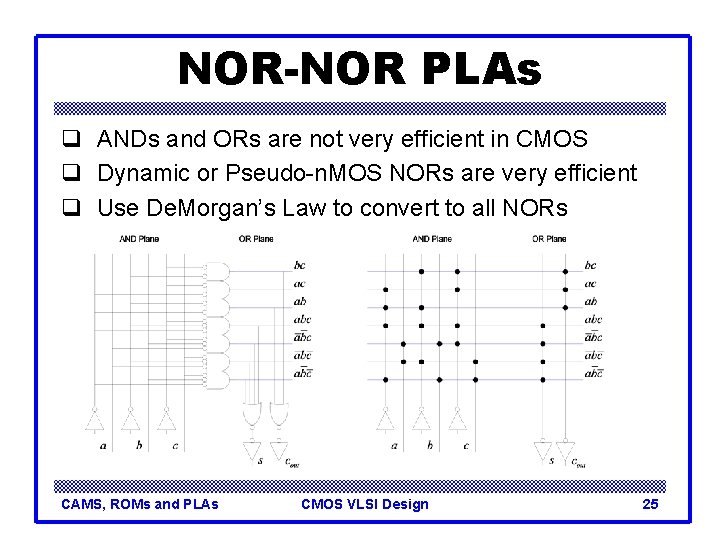
NOR-NOR PLAs q ANDs and ORs are not very efficient in CMOS q Dynamic or Pseudo-n. MOS NORs are very efficient q Use De. Morgan’s Law to convert to all NORs CAMS, ROMs and PLAs CMOS VLSI Design 25

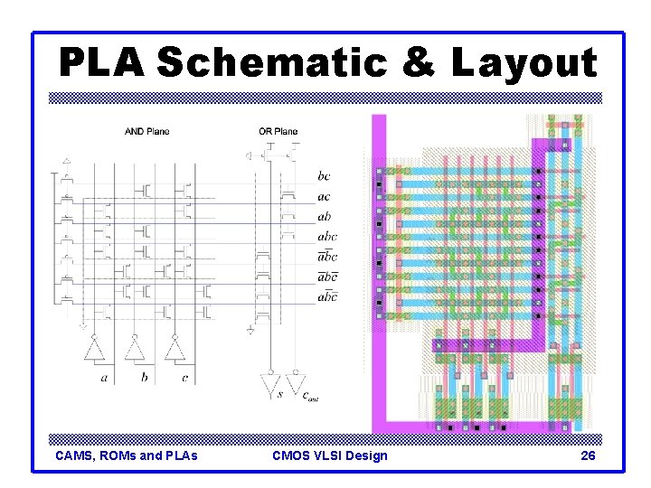
PLA Schematic & Layout CAMS, ROMs and PLAs CMOS VLSI Design 26

PLAs vs. ROMs q The OR plane of the PLA is like the ROM array q The AND plane of the PLA is like the ROM decoder q PLAs are more flexible than ROMs – No need to have 2 n rows for n inputs – Only generate the minterms that are needed – Take advantage of logic simplification CAMS, ROMs and PLAs CMOS VLSI Design 27

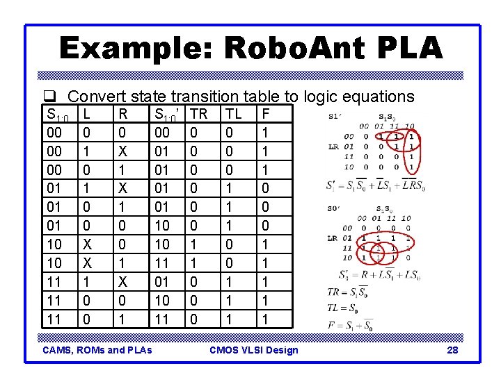
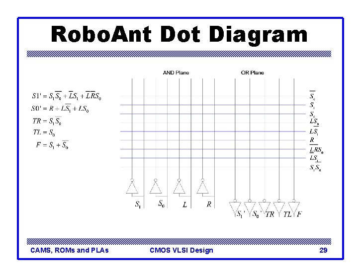
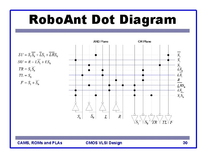
Example: Robo. Ant PLA q Convert state transition table to logic equations S 1: 0 00 01 01 01 10 10 11 11 11 L 0 1 0 0 X X 1 0 0 R 0 X 1 0 0 1 X 0 1 CAMS, ROMs and PLAs S 1: 0’ 00 01 01 10 10 11 01 10 11 TR 0 0 0 1 1 0 0 0 TL 0 0 0 1 1 1 F 1 1 1 0 0 0 1 1 1 CMOS VLSI Design 28

Robo. Ant Dot Diagram CAMS, ROMs and PLAs CMOS VLSI Design 29

Robo. Ant Dot Diagram CAMS, ROMs and PLAs CMOS VLSI Design 30