ECE 224 a Process and Design Rules q
- Slides: 65

ECE 224 a Process and Design Rules q Process Overview q Device Fabrication Limits q Derived Layers q Self Alignment/Dual Damascene/CMP q Design Rules § Resolution/Step Coverage/Process § Electrical/Reliability/Mechanical Stress F. EE 141 Brewer, adapted from MOSIS Data, Digital Integrated Circuits 2 nd 1 Manufacturing

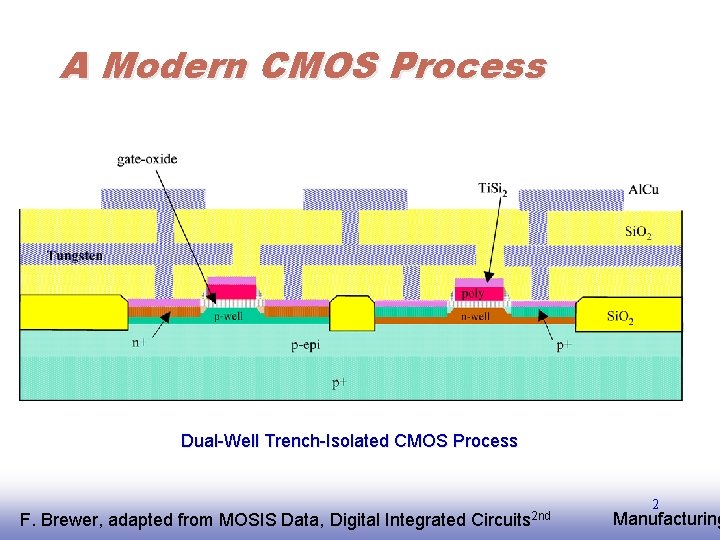
A Modern CMOS Process Dual-Well Trench-Isolated CMOS Process F. EE 141 Brewer, adapted from MOSIS Data, Digital Integrated Circuits 2 nd 2 Manufacturing

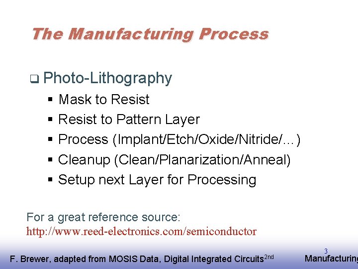
The Manufacturing Process q Photo-Lithography § § § Mask to Resist to Pattern Layer Process (Implant/Etch/Oxide/Nitride/…) Cleanup (Clean/Planarization/Anneal) Setup next Layer for Processing For a great reference source: http: //www. reed-electronics. com/semiconductor F. EE 141 Brewer, adapted from MOSIS Data, Digital Integrated Circuits 2 nd 3 Manufacturing

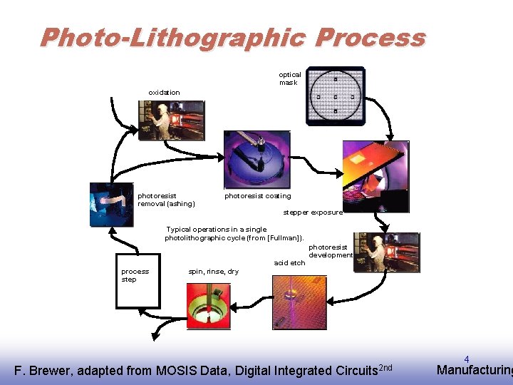
Photo-Lithographic Process optical mask oxidation photoresist removal (ashing) photoresist coating stepper exposure Typical operations in a single photolithographic cycle (from [Fullman]). photoresist development acid etch process step spin, rinse, dry F. EE 141 Brewer, adapted from MOSIS Data, Digital Integrated Circuits 2 nd 4 Manufacturing

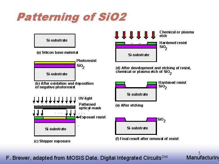
Patterning of Si. O 2 Chemical or plasma etch Si-substrate Hardened resist Si. O 2 (a) Silicon base material Si-substrate Photoresist Si. O 2 Si-substrate (d) After development and etching of resist, chemical or plasma etch of Si. O 2 Hardened resist Si. O 2 (b) After oxidation and deposition of negative photoresist UV-light Patterned optical mask Si-substrate (e) After etching Exposed resist Si-substrate (c) Stepper exposure Si. O 2 Si-substrate (f) Final result after removal of resist F. EE 141 Brewer, adapted from MOSIS Data, Digital Integrated Circuits 2 nd 5 Manufacturing

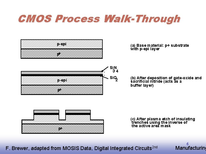
CMOS Process Walk-Through p-epi (a) Base material: p+ substrate with p-epi layer p+ Si. N 34 p-epi p+ p+ Si. O 2 (b) After deposition of gate-oxide and sacrificial nitride (acts as a buffer layer) (c) After plasma etch of insulating trenches using the inverse of the active area mask F. EE 141 Brewer, adapted from MOSIS Data, Digital Integrated Circuits 2 nd 6 Manufacturing

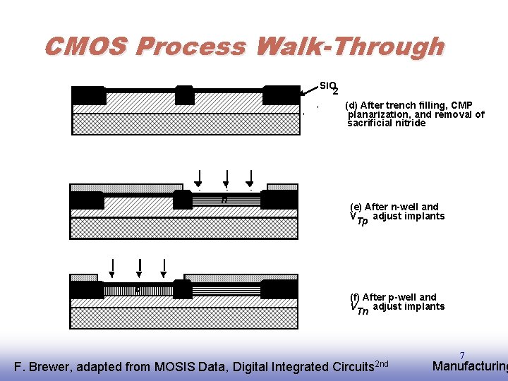
CMOS Process Walk-Through Si. O 2 (d) After trench filling, CMP planarization, and removal of sacrificial nitride n p F. EE 141 Brewer, adapted from MOSIS Data, Digital Integrated (e) After n-well and V adjust implants Tp (f) After p-well and V adjust implants Tn Circuits 2 nd 7 Manufacturing

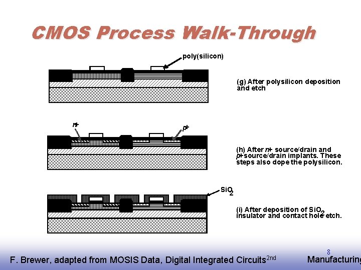
CMOS Process Walk-Through poly(silicon) (g) After polysilicon deposition and etch n+ p+ (h) After n+ source/drain and p+ source/drain implants. These steps also dope the polysilicon. Si. O 2 (i) After deposition of Si. O insulator and contact hole 2 etch. F. EE 141 Brewer, adapted from MOSIS Data, Digital Integrated Circuits 2 nd 8 Manufacturing

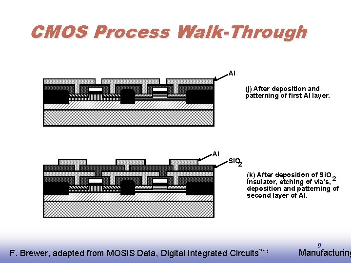
CMOS Process Walk-Through Al (j) After deposition and patterning of first Al layer. Al Si. O 2 (k) After deposition of Si. O insulator, etching of via’s, 2 deposition and patterning of second layer of Al. F. EE 141 Brewer, adapted from MOSIS Data, Digital Integrated Circuits 2 nd 9 Manufacturing

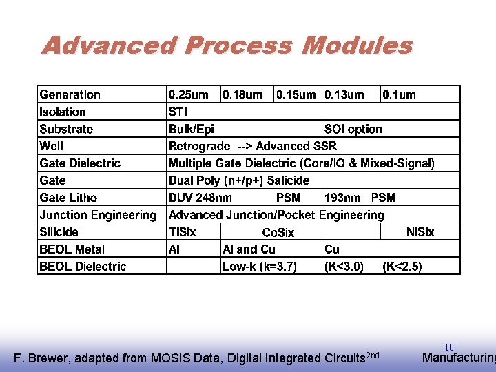
Advanced Process Modules F. EE 141 Brewer, adapted from MOSIS Data, Digital Integrated Circuits 2 nd 10 Manufacturing

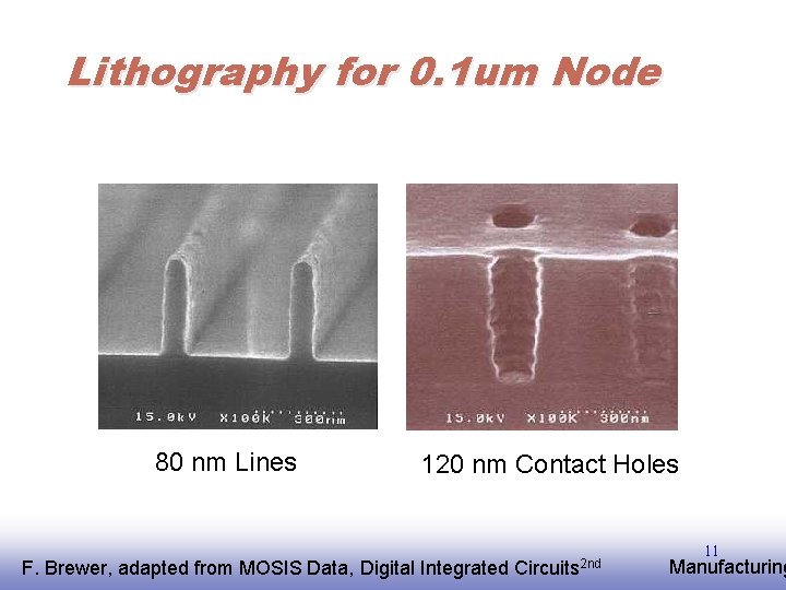
Lithography for 0. 1 um Node 80 nm Lines 120 nm Contact Holes F. EE 141 Brewer, adapted from MOSIS Data, Digital Integrated Circuits 2 nd 11 Manufacturing

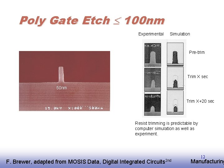
Poly Gate Etch 100 nm Experimental Simulation Pre-trim Trim X sec 50 nm Trim X+20 sec Resist trimming is predictable by computer simulation as well as experiment. F. EE 141 Brewer, adapted from MOSIS Data, Digital Integrated Circuits 2 nd 12 Manufacturing

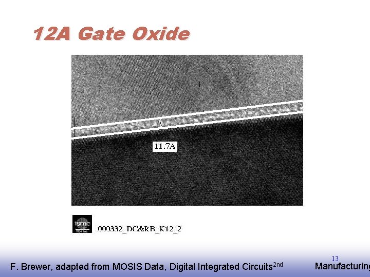
12 A Gate Oxide F. EE 141 Brewer, adapted from MOSIS Data, Digital Integrated Circuits 2 nd 13 Manufacturing

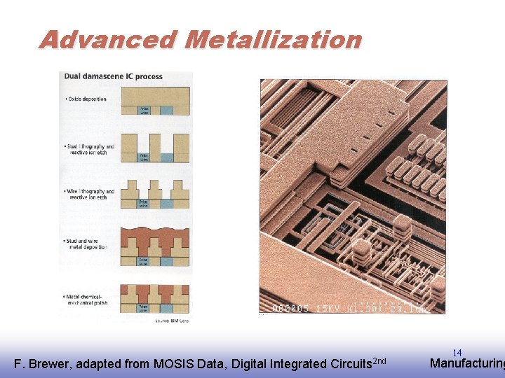
Advanced Metallization F. EE 141 Brewer, adapted from MOSIS Data, Digital Integrated Circuits 2 nd 14 Manufacturing

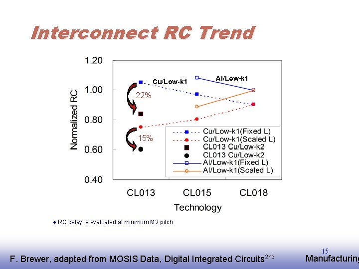
Interconnect RC Trend Cu/Low-k 1 Al/Low-k 1 22% 15% l RC delay is evaluated at minimum M 2 pitch F. EE 141 Brewer, adapted from MOSIS Data, Digital Integrated Circuits 2 nd 15 Manufacturing

Design Rules q What can be fabricated? § Resolution Limits – Light Source (357 nm, 254 nm, 193 nm, ? ) – Contact/Phase Masking – Surface State (Reflection/Scattering) § Material Limits – Step Coverage – Porosity/Defect Propagation – Mechanical/Thermal Stress F. EE 141 Brewer, adapted from MOSIS Data, Digital Integrated Circuits 2 nd 16 Manufacturing

Design Rules II § Electrical Limits – Electrical Fields (MV/cm)! – Parasitic Conductivity/Devices (Latchup/ESD) – Joule Heating (Electro-Migration) § Defect Probability – Contact/Via Replication – Grid-Based Power/Ground Networks § Advance Lithography – Rule Explosion/Failure of Locality – CMP Area Rules/Antenna Rules F. EE 141 Brewer, adapted from MOSIS Data, Digital Integrated Circuits 2 nd 17 Manufacturing

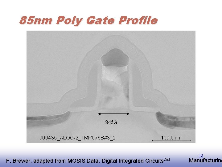
85 nm Poly Gate Profile 845 A F. EE 141 Brewer, adapted from MOSIS Data, Digital Integrated Circuits 2 nd 18 Manufacturing

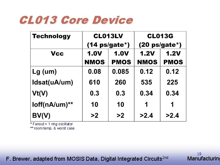
CL 013 Core Device * Fanout = 1 ring oscillator ** room temp. & worst case. F. EE 141 Brewer, adapted from MOSIS Data, Digital Integrated Circuits 2 nd 19 Manufacturing

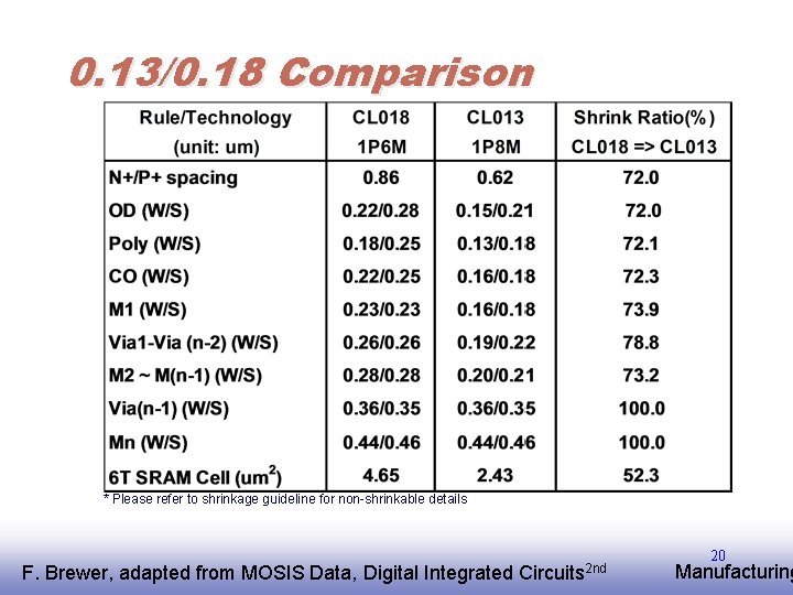
0. 13/0. 18 Comparison * Please refer to shrinkage guideline for non-shrinkable details F. EE 141 Brewer, adapted from MOSIS Data, Digital Integrated Circuits 2 nd 20 Manufacturing

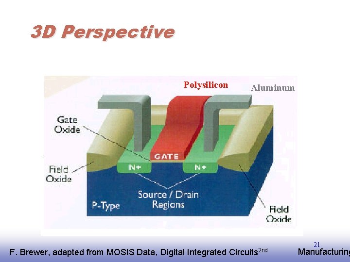
3 D Perspective Polysilicon F. EE 141 Brewer, adapted from MOSIS Data, Digital Integrated Aluminum Circuits 2 nd 21 Manufacturing

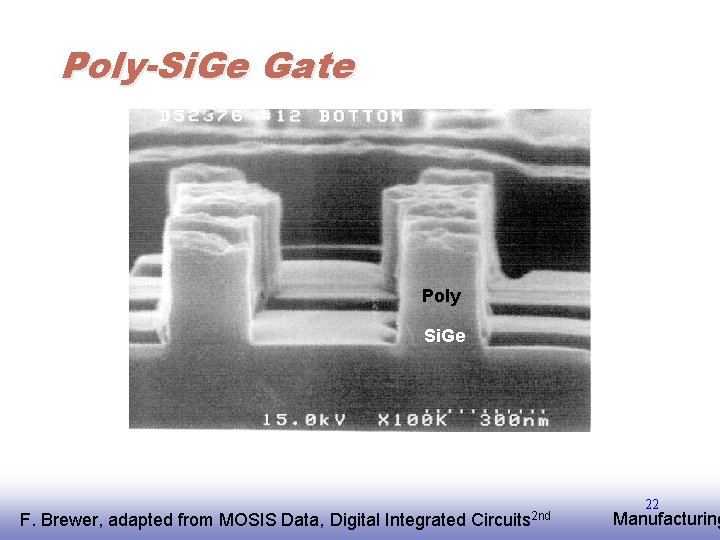
Poly-Si. Ge Gate Poly Si. Ge F. EE 141 Brewer, adapted from MOSIS Data, Digital Integrated Circuits 2 nd 22 Manufacturing

Design Rules III Interface twixt designer and process engineer q Unit dimension: Minimum Feature Size § scalable design rules: lambda § absolute dimensions: (Vendor rules) q q Process Design Layers § Derived Layers F. EE 141 Brewer, adapted from MOSIS Data, Digital Integrated Circuits 2 nd 23 Manufacturing

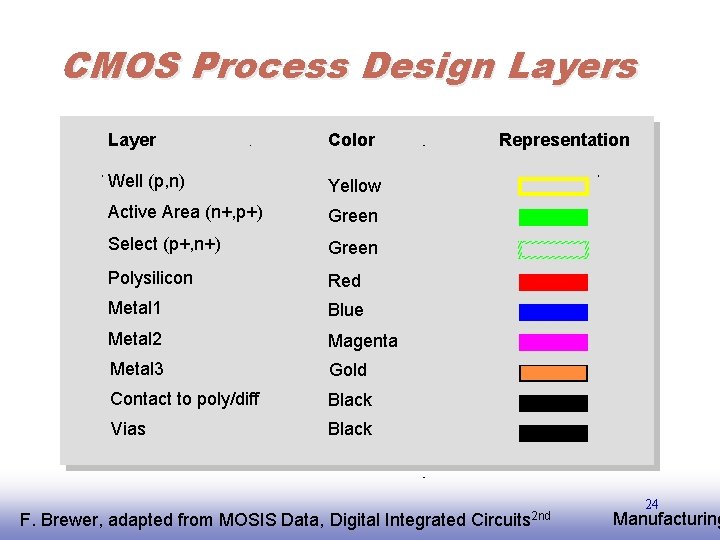
CMOS Process Design Layers Layer Color Well (p, n) Yellow Active Area (n+, p+) Green Select (p+, n+) Green Polysilicon Red Metal 1 Blue Metal 2 Magenta Metal 3 Gold Contact to poly/diff Black Vias Black F. EE 141 Brewer, adapted from MOSIS Data, Digital Integrated Representation Circuits 2 nd 24 Manufacturing

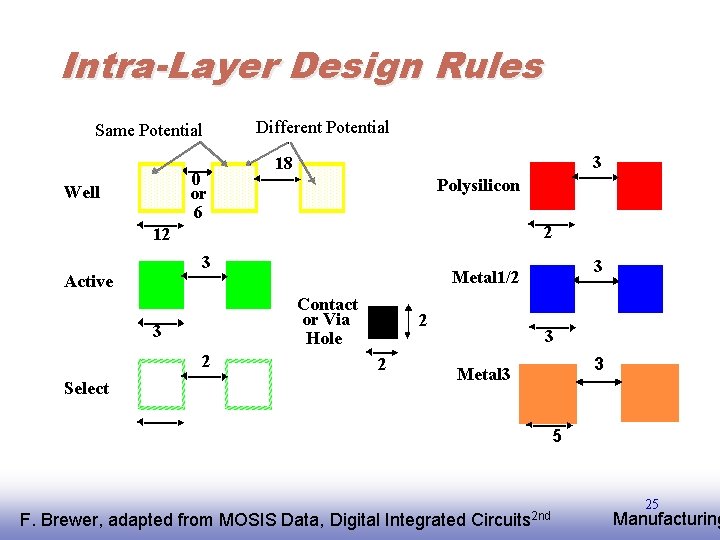
Intra-Layer Design Rules Same Potential 0 or 6 Well Different Potential 3 18 Polysilicon 2 12 3 Active Contact or Via Hole 3 2 Select 3 Metal 1/2 2 2 3 3 Metal 3 5 F. EE 141 Brewer, adapted from MOSIS Data, Digital Integrated Circuits 2 nd 25 Manufacturing

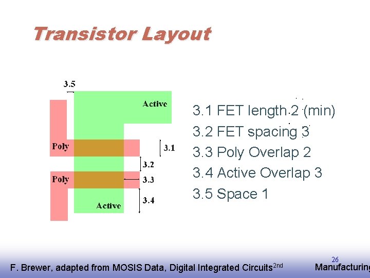
Transistor Layout 3. 1 FET length 2 (min) 3. 2 FET spacing 3 3. 3 Poly Overlap 2 3. 4 Active Overlap 3 3. 5 Space 1 F. EE 141 Brewer, adapted from MOSIS Data, Digital Integrated Circuits 2 nd 26 Manufacturing

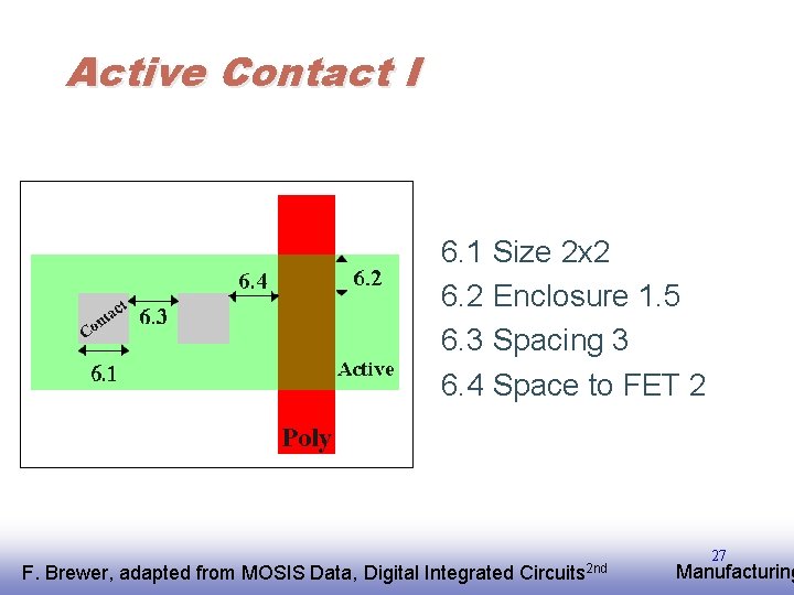
Active Contact I 6. 1 Size 2 x 2 6. 2 Enclosure 1. 5 6. 3 Spacing 3 6. 4 Space to FET 2 F. EE 141 Brewer, adapted from MOSIS Data, Digital Integrated Circuits 2 nd 27 Manufacturing

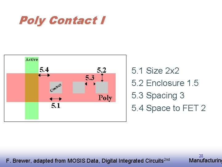
Poly Contact I 5. 1 Size 2 x 2 5. 2 Enclosure 1. 5 5. 3 Spacing 3 5. 4 Space to FET 2 F. EE 141 Brewer, adapted from MOSIS Data, Digital Integrated Circuits 2 nd 28 Manufacturing

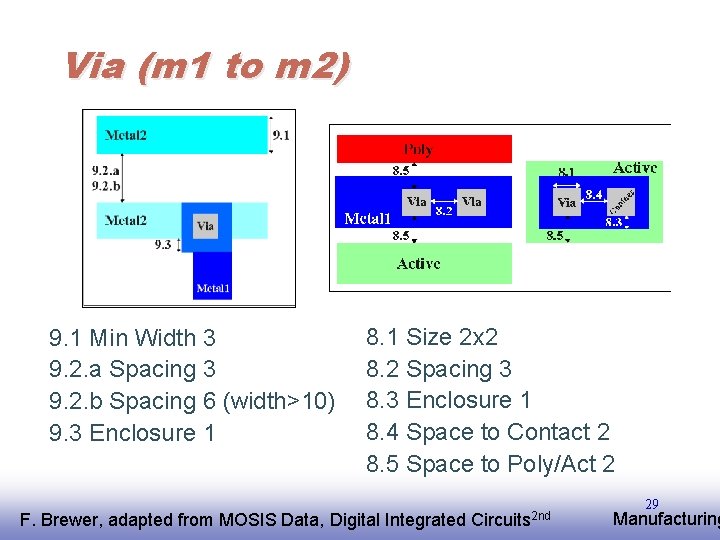
Via (m 1 to m 2) 9. 1 Min Width 3 9. 2. a Spacing 3 9. 2. b Spacing 6 (width>10) 9. 3 Enclosure 1 8. 1 Size 2 x 2 8. 2 Spacing 3 8. 3 Enclosure 1 8. 4 Space to Contact 2 8. 5 Space to Poly/Act 2 F. EE 141 Brewer, adapted from MOSIS Data, Digital Integrated Circuits 2 nd 29 Manufacturing

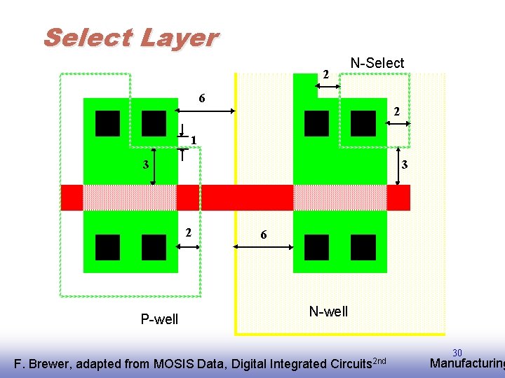
Select Layer N-Select 2 6 2 1 3 3 2 P-well 6 N-well F. EE 141 Brewer, adapted from MOSIS Data, Digital Integrated Circuits 2 nd 30 Manufacturing

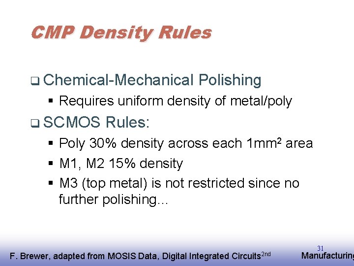
CMP Density Rules q Chemical-Mechanical Polishing § Requires uniform density of metal/poly q SCMOS Rules: § Poly 30% density across each 1 mm 2 area § M 1, M 2 15% density § M 3 (top metal) is not restricted since no further polishing… F. EE 141 Brewer, adapted from MOSIS Data, Digital Integrated Circuits 2 nd 31 Manufacturing

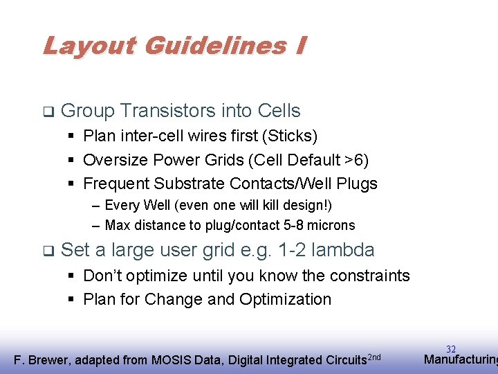
Layout Guidelines I q Group Transistors into Cells § Plan inter-cell wires first (Sticks) § Oversize Power Grids (Cell Default >6) § Frequent Substrate Contacts/Well Plugs – Every Well (even one will kill design!) – Max distance to plug/contact 5 -8 microns q Set a large user grid e. g. 1 -2 lambda § Don’t optimize until you know the constraints § Plan for Change and Optimization F. EE 141 Brewer, adapted from MOSIS Data, Digital Integrated Circuits 2 nd 32 Manufacturing

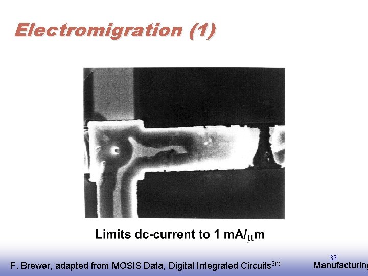
Electromigration (1) F. EE 141 Brewer, adapted from MOSIS Data, Digital Integrated Circuits 2 nd 33 Manufacturing

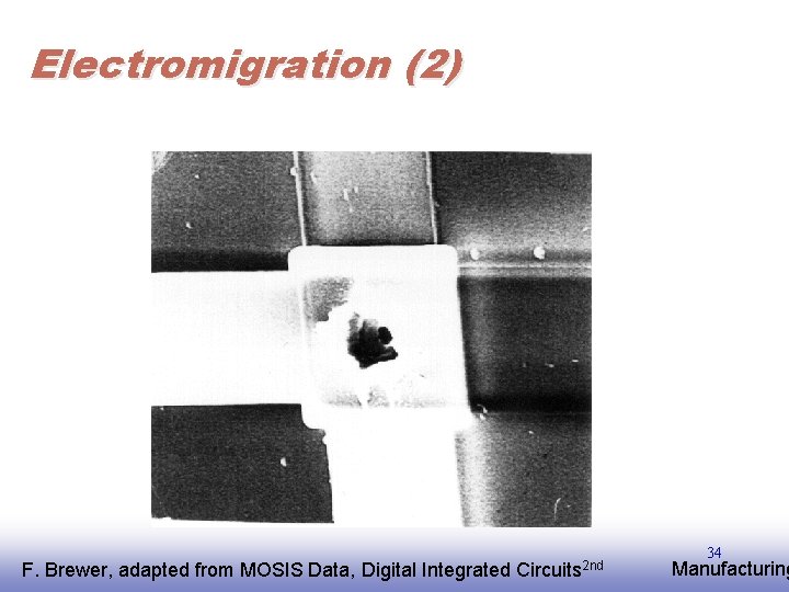
Electromigration (2) F. EE 141 Brewer, adapted from MOSIS Data, Digital Integrated Circuits 2 nd 34 Manufacturing

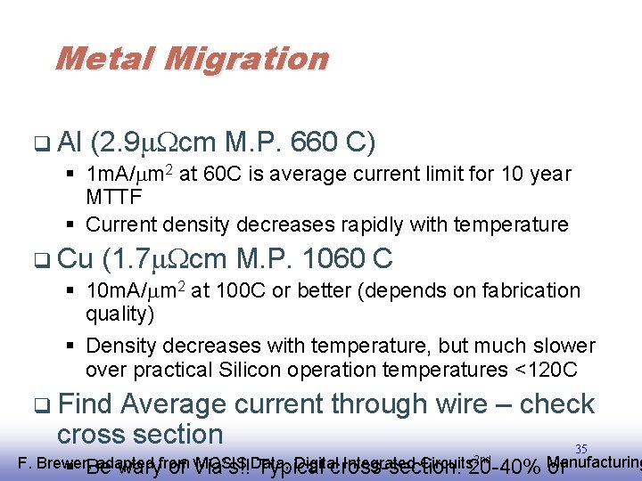
Metal Migration q Al (2. 9 Wcm M. P. 660 C) § 1 m. A/ m 2 at 60 C is average current limit for 10 year MTTF § Current density decreases rapidly with temperature q Cu (1. 7 Wcm M. P. 1060 C § 10 m. A/ m 2 at 100 C or better (depends on fabrication quality) § Density decreases with temperature, but much slower over practical Silicon operation temperatures <120 C q Find Average current through wire – check cross section 35 2 nd Manufacturing F. EE 141 Brewer, adapted MOSIS Data, Digital Integrated Circuits 20 -40% § Be waryfrom of Via’s!! Typical cross-section: of

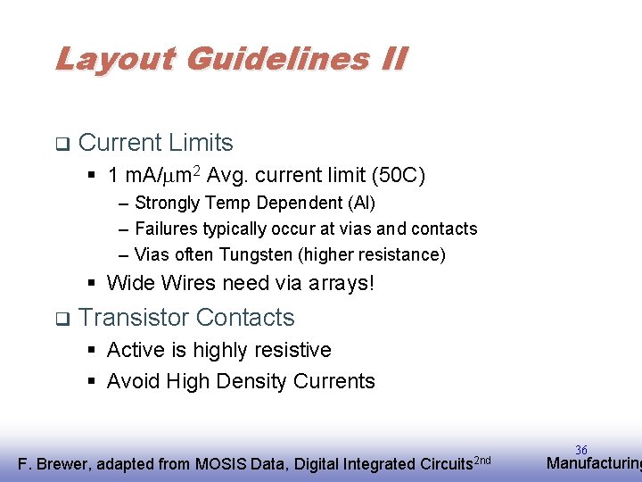
Layout Guidelines II q Current Limits § 1 m. A/ m 2 Avg. current limit (50 C) – Strongly Temp Dependent (Al) – Failures typically occur at vias and contacts – Vias often Tungsten (higher resistance) § Wide Wires need via arrays! q Transistor Contacts § Active is highly resistive § Avoid High Density Currents F. EE 141 Brewer, adapted from MOSIS Data, Digital Integrated Circuits 2 nd 36 Manufacturing

Pads F. EE 141 Brewer, adapted from MOSIS Data, Digital Integrated Circuits 2 nd 37 Manufacturing

Pads-- Chip to Board Interface q Pads drive large Capacitances § 5 pf minimum to much larger § Rise time control q Board Impeadance and Noise § L d. I/dt Noise q Coupling to Power Distribution q ESD F. EE 141 Brewer, adapted from MOSIS Data, Digital Integrated Circuits 2 nd 38 Manufacturing

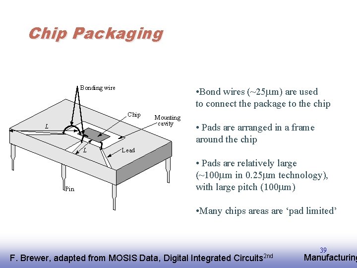
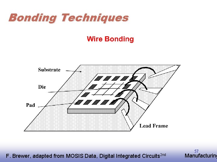
Chip Packaging Bonding wire • Bond wires (~25 m) are used to connect the package to the chip Chip L L Pin Mounting cavity • Pads are arranged in a frame around the chip Lead • Pads are relatively large (~100 m in 0. 25 m technology), with large pitch (100 m) • Many chips areas are ‘pad limited’ F. EE 141 Brewer, adapted from MOSIS Data, Digital Integrated Circuits 2 nd 39 Manufacturing

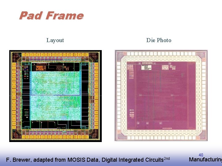
Pad Frame Layout F. EE 141 Brewer, adapted from MOSIS Data, Digital Integrated Die Photo Circuits 2 nd 40 Manufacturing

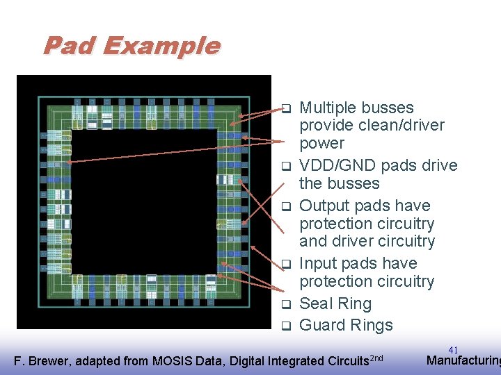
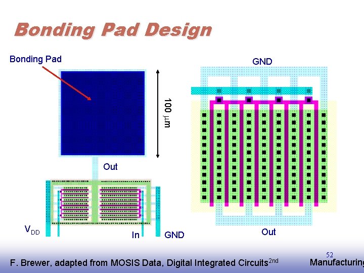
Pad Example q q q Multiple busses provide clean/driver power VDD/GND pads drive the busses Output pads have protection circuitry and driver circuitry Input pads have protection circuitry Seal Ring Guard Rings F. EE 141 Brewer, adapted from MOSIS Data, Digital Integrated Circuits 2 nd 41 Manufacturing

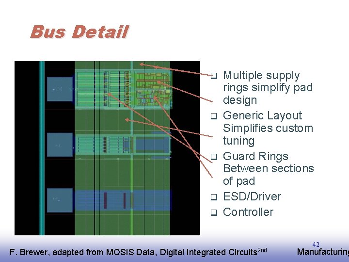
Bus Detail q q q Multiple supply rings simplify pad design Generic Layout Simplifies custom tuning Guard Rings Between sections of pad ESD/Driver Controller F. EE 141 Brewer, adapted from MOSIS Data, Digital Integrated Circuits 2 nd 42 Manufacturing

Seal Ring q q Seal Ring is essentially a guard ring with metal layers and contacts placed to lower overglass to substrate evenly at chip boundary Hermetic seal of chip from atmosphere and other contamination F. EE 141 Brewer, adapted from MOSIS Data, Digital Integrated Circuits 2 nd 43 Manufacturing

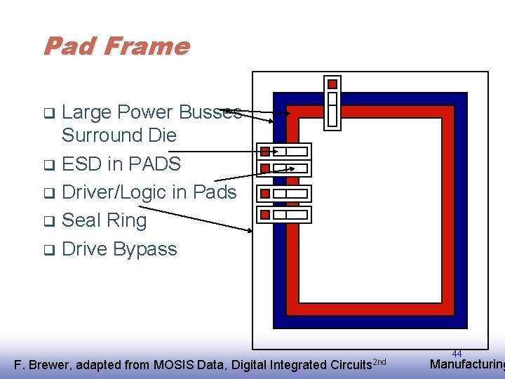
Pad Frame Large Power Busses Surround Die q ESD in PADS q Driver/Logic in Pads q Seal Ring q Drive Bypass q F. EE 141 Brewer, adapted from MOSIS Data, Digital Integrated Circuits 2 nd 44 Manufacturing

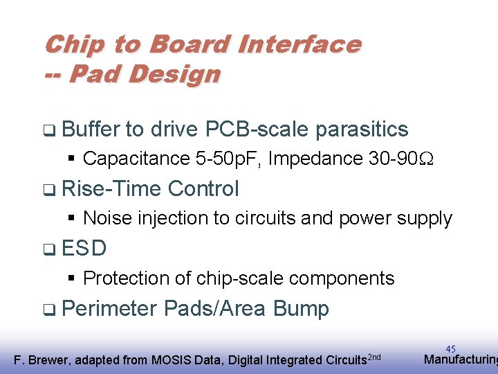
Chip to Board Interface -- Pad Design q Buffer to drive PCB-scale parasitics § Capacitance 5 -50 p. F, Impedance 30 -90 W q Rise-Time Control § Noise injection to circuits and power supply q ESD § Protection of chip-scale components q Perimeter Pads/Area Bump F. EE 141 Brewer, adapted from MOSIS Data, Digital Integrated Circuits 2 nd 45 Manufacturing

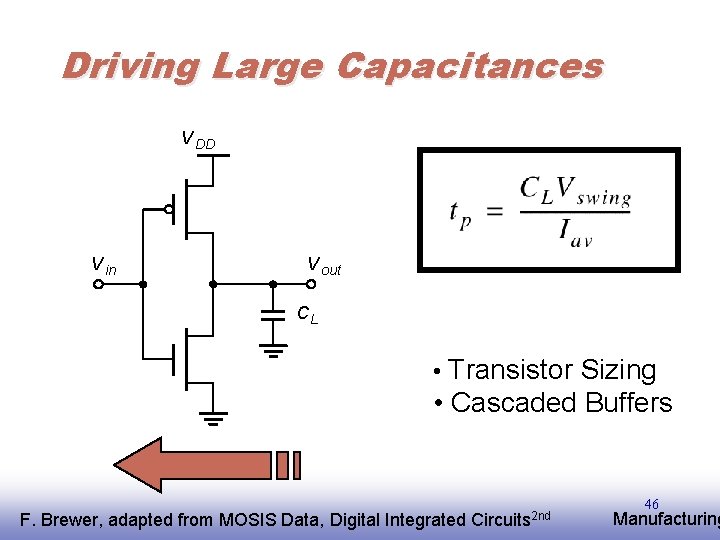
Driving Large Capacitances V DD V in V out CL • Transistor Sizing • Cascaded Buffers F. EE 141 Brewer, adapted from MOSIS Data, Digital Integrated Circuits 2 nd 46 Manufacturing

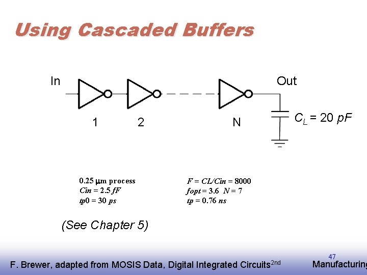
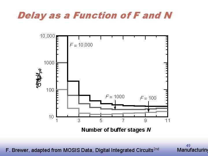
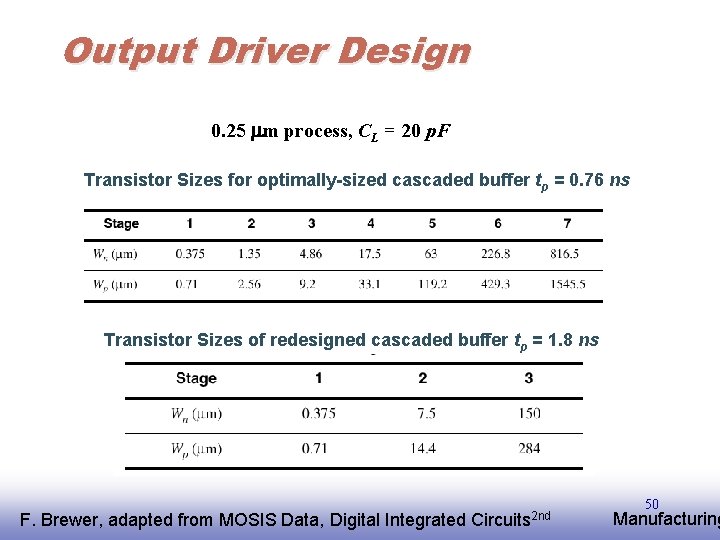
Using Cascaded Buffers In Out 1 2 0. 25 mm process Cin = 2. 5 f. F tp 0 = 30 ps N CL = 20 p. F F = CL/Cin = 8000 fopt = 3. 6 N = 7 tp = 0. 76 ns (See Chapter 5) F. EE 141 Brewer, adapted from MOSIS Data, Digital Integrated Circuits 2 nd 47 Manufacturing

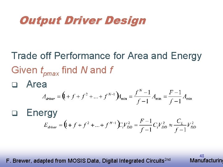
Output Driver Design Trade off Performance for Area and Energy Given tpmax find N and f q Area q Energy F. EE 141 Brewer, adapted from MOSIS Data, Digital Integrated Circuits 2 nd 48 Manufacturing

Delay as a Function of F and N 10, 000 F = 10, 000 tp/tp 0 1000 p t/0 tp 100 F = 1000 10 1 3 5 7 F = 100 9 11 Number of buffer stages N F. EE 141 Brewer, adapted from MOSIS Data, Digital Integrated Circuits 2 nd 49 Manufacturing

Output Driver Design 0. 25 mm process, CL = 20 p. F Transistor Sizes for optimally-sized cascaded buffer tp = 0. 76 ns Transistor Sizes of redesigned cascaded buffer tp = 1. 8 ns F. EE 141 Brewer, adapted from MOSIS Data, Digital Integrated Circuits 2 nd 50 Manufacturing

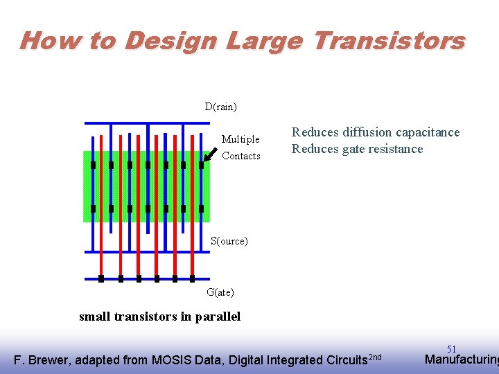
How to Design Large Transistors D(rain) Multiple Contacts Reduces diffusion capacitance Reduces gate resistance S(ource) G(ate) small transistors in parallel F. EE 141 Brewer, adapted from MOSIS Data, Digital Integrated Circuits 2 nd 51 Manufacturing

Bonding Pad Design Bonding Pad GND 100 m Out VDD In GND F. EE 141 Brewer, adapted from MOSIS Data, Digital Integrated Out Circuits 2 nd 52 Manufacturing

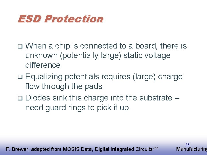
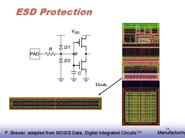
ESD Protection When a chip is connected to a board, there is unknown (potentially large) static voltage difference q Equalizing potentials requires (large) charge flow through the pads q Diodes sink this charge into the substrate – need guard rings to pick it up. q F. EE 141 Brewer, adapted from MOSIS Data, Digital Integrated Circuits 2 nd 53 Manufacturing

ESD Protection Diode F. EE 141 Brewer, adapted from MOSIS Data, Digital Integrated Circuits 2 nd 54 Manufacturing

Packaging F. EE 141 Brewer, adapted from MOSIS Data, Digital Integrated Circuits 2 nd 55 Manufacturing

Packaging Requirements q Electrical: Low parasitics q Mechanical: Reliable and robust q Thermal: Efficient heat removal q Economical: Cheap F. EE 141 Brewer, adapted from MOSIS Data, Digital Integrated Circuits 2 nd 56 Manufacturing

Bonding Techniques F. EE 141 Brewer, adapted from MOSIS Data, Digital Integrated Circuits 2 nd 57 Manufacturing

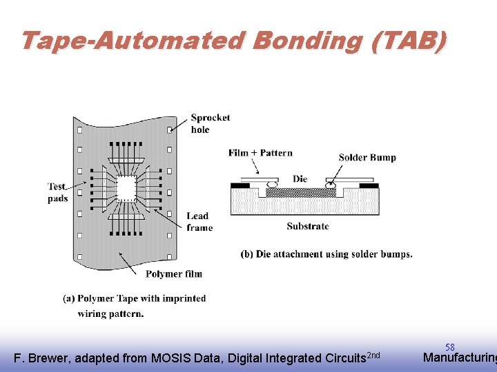
Tape-Automated Bonding (TAB) F. EE 141 Brewer, adapted from MOSIS Data, Digital Integrated Circuits 2 nd 58 Manufacturing

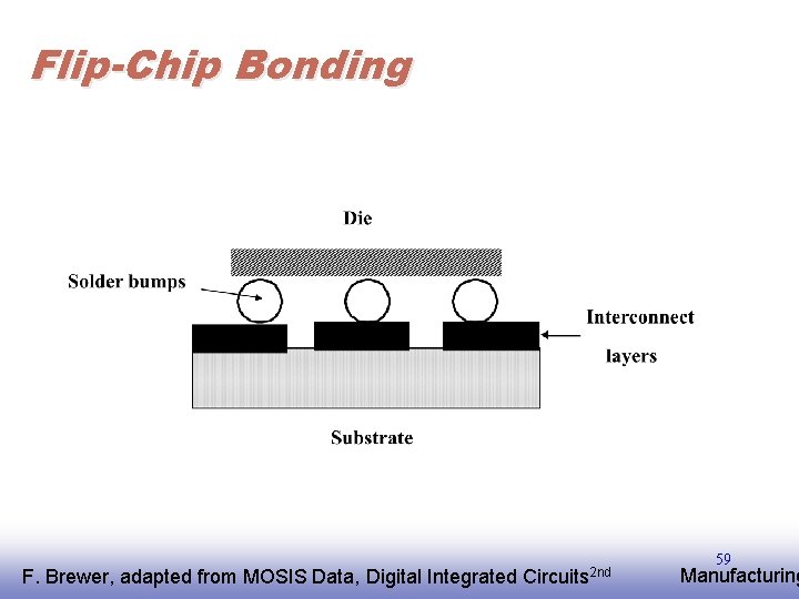
Flip-Chip Bonding F. EE 141 Brewer, adapted from MOSIS Data, Digital Integrated Circuits 2 nd 59 Manufacturing

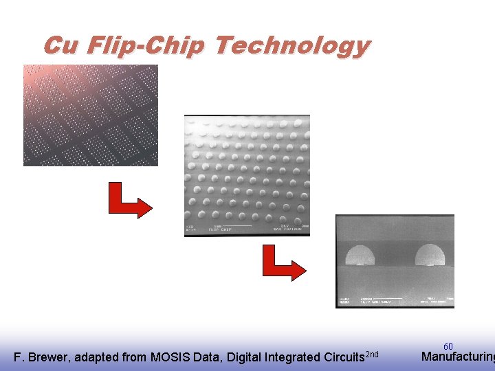
Cu Flip-Chip Technology F. EE 141 Brewer, adapted from MOSIS Data, Digital Integrated Circuits 2 nd 60 Manufacturing

Package-to-Board Interconnect F. EE 141 Brewer, adapted from MOSIS Data, Digital Integrated Circuits 2 nd 61 Manufacturing

Package Types F. EE 141 Brewer, adapted from MOSIS Data, Digital Integrated Circuits 2 nd 62 Manufacturing

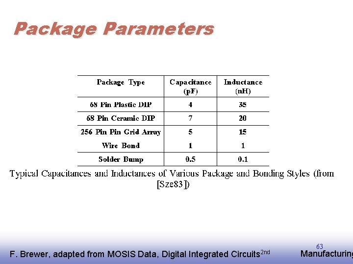
Package Parameters F. EE 141 Brewer, adapted from MOSIS Data, Digital Integrated Circuits 2 nd 63 Manufacturing

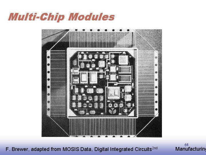
Multi-Chip Modules F. EE 141 Brewer, adapted from MOSIS Data, Digital Integrated Circuits 2 nd 64 Manufacturing

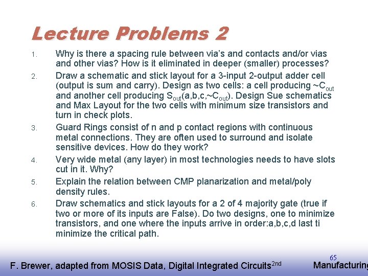
Lecture Problems 2 1. 2. 3. 4. 5. 6. Why is there a spacing rule between via’s and contacts and/or vias and other vias? How is it eliminated in deeper (smaller) processes? Draw a schematic and stick layout for a 3 -input 2 -output adder cell (output is sum and carry). Design as two cells: a cell producing ~Cout and another cell producing Sout(a, b, c, ~Cout). Design Sue schematics and Max Layout for the two cells with minimum size transistors and turn in check plots. Guard Rings consist of n and p contact regions with continuous metal connections. They are often used to surround and isolate sensitive devices. How do they work? Very wide metal (any layer) in most technologies needs to have slots cut in it. Why? Explain the relation between CMP planarization and metal/poly density rules. Draw schematics and stick layouts for a 2 of 4 majority gate (true if two or more of its inputs are False). Do two designs, one to minimize transistors, and one where the inputs arrive in order: a, b, c, d last ti minimize the critical path. F. EE 141 Brewer, adapted from MOSIS Data, Digital Integrated Circuits 2 nd 65 Manufacturing