EELE 414 Introduction to VLSI Design Module 2
- Slides: 147

EELE 414 – Introduction to VLSI Design Module #2 – MOSFET Operation • Agenda 1. MOSFET Operation - Device Physics - MOSFET Structure - IV Characteristics - Scaling - Small Geometry Effects - Capacitance • Announcements 1. Read Chapter 3 EELE 414 – Introduction to VLSI Design Module #2 Page 1

MOSFET Operation • MOSFET - Metal Oxide Semiconductor Field Effect Transistor - we need to understand the detailed operation of the MOSFET in order to use it to build larger blocks such as Inverters, NAND gates, adders, etc… - we will cover theory of the device physics, energy bands, and circuit operation - we will do homework to analyze the behavior by hand - in the real world, we typically use SPICE simulations to quickly analyze the MOSFET behavior - but we need to understand what SPICE is calculating or: 1) we won’t be able to understand performance problems 2) we won’t be able to troubleshoot (is it the tool, is it the circuit, is it the process? ) EELE 414 – Introduction to VLSI Design Module #2 Page 2

Semiconductors • Semiconductors - a semiconductor is a solid material which acts as an insulator at absolute zero. As the temperature increases, a semiconductor begins to conduct - a single element can be a semiconductor: Carbon (C), Silicon (Si) - a compound material can also form a semiconductors (i. e. , two or more materials chemically bonded) Gallium Arsenide (Ga. As), Indium Phosphide (In. P) - an alloy material can also form semiconductors (i. e. , a mixture of elements of which one is a metal): Silicon Germanium (Si. Ge), Aluminum Gallium Arsenide (Al. Ga. As) - Silicon is the most widely used semiconductors for VLSI circuits due to: - it is the 2 nd most abundant element (25. 7%) of the earth’s crust (after oxygen) - it remains a semiconductor at a higher temperature - it can be oxidized very easily EELE 414 – Introduction to VLSI Design Module #2 Page 3

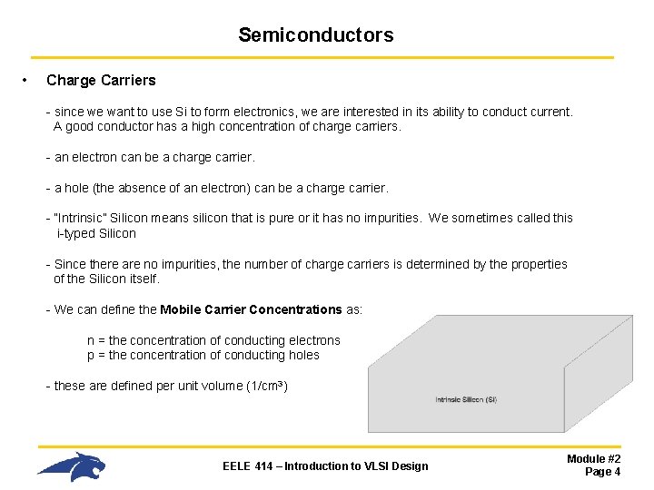
Semiconductors • Charge Carriers - since we want to use Si to form electronics, we are interested in its ability to conduct current. A good conductor has a high concentration of charge carriers. - an electron can be a charge carrier. - a hole (the absence of an electron) can be a charge carrier. - “Intrinsic” Silicon means silicon that is pure or it has no impurities. We sometimes called this i-typed Silicon - Since there are no impurities, the number of charge carriers is determined by the properties of the Silicon itself. - We can define the Mobile Carrier Concentrations as: n = the concentration of conducting electrons p = the concentration of conducting holes - these are defined per unit volume (1/cm 3) EELE 414 – Introduction to VLSI Design Module #2 Page 4

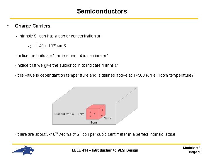
Semiconductors • Charge Carriers - Intrinsic Silicon has a carrier concentration of : ni = 1. 45 x 1010 cm-3 - notice the units are “carriers per cubic centimeter” - notice that we give the subscript “i” to indicate “intrinsic” - this value is dependant on temperature and is defined above at T=300 K (i. e. , room temperature) - there about 5 x 10²² Atoms of Silicon per cubic centimeter in a perfect intrinsic lattice EELE 414 – Introduction to VLSI Design Module #2 Page 5

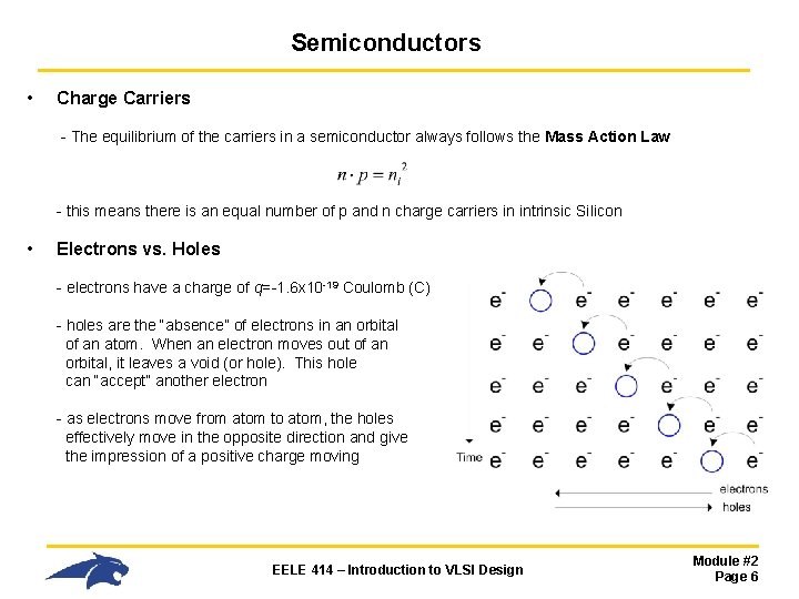
Semiconductors • Charge Carriers - The equilibrium of the carriers in a semiconductor always follows the Mass Action Law - this means there is an equal number of p and n charge carriers in intrinsic Silicon • Electrons vs. Holes - electrons have a charge of q=-1. 6 x 10 -19 Coulomb (C) - holes are the “absence” of electrons in an orbital of an atom. When an electron moves out of an orbital, it leaves a void (or hole). This hole can “accept” another electron - as electrons move from atom to atom, the holes effectively move in the opposite direction and give the impression of a positive charge moving EELE 414 – Introduction to VLSI Design Module #2 Page 6

Energy Bands • Energy Bands - the mobility of a semiconductor increases as its temperature increase. - Increasing the mobility of a semiconductor eventually turns the material into a conductor. - this is of interest to electronics because we can control the flow of current - we can also cause conduction using an applied voltage to provide the energy - we are interested in how much energy it takes to alter the behavior of the material - Energy Band Diagrams are a graphical way to describe the energy needed to change the behavior of a material. EELE 414 – Introduction to VLSI Design Module #2 Page 7

Energy Bands • Energy Bands - Quantum Mechanics created the concept of bands to represent the levels of energy that are present at each “state” of an atom. - the electrons on an atom occupy these energy states - For a given number of electrons in an atom, we begin filling in the energy bands from lowest to highest energy until all of the electrons have been used. - electrons only exist in the bands. By convention, electrons are forbidden from existing in between bands - there is a finite amount of energy that exists to move an electron from one band to another - if given enough energy (via heat or E-fields), electrons can receive enough energy to jump to a higher energy band. EELE 414 – Introduction to VLSI Design Module #2 Page 8

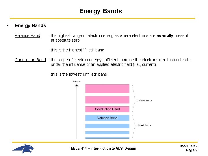
Energy Bands • Energy Bands Valence Band : the highest range of electron energies where electrons are normally present at absolute zero. : this is the highest “filled” band Conduction Band : the range of electron energy sufficient to make the electrons free to accelerate under the influence of an applied electric field (i. e. , current). : this is the lowest “unfilled” band EELE 414 – Introduction to VLSI Design Module #2 Page 9

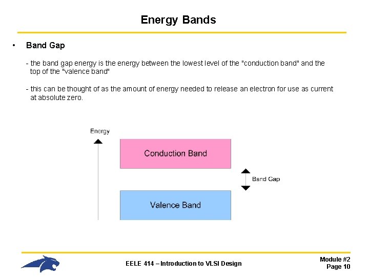
Energy Bands • Band Gap - the band gap energy is the energy between the lowest level of the "conduction band" and the top of the "valence band" - this can be thought of as the amount of energy needed to release an electron for use as current at absolute zero. EELE 414 – Introduction to VLSI Design Module #2 Page 10

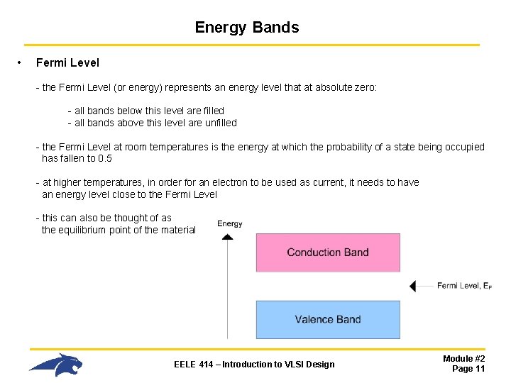
Energy Bands • Fermi Level - the Fermi Level (or energy) represents an energy level that at absolute zero: - all bands below this level are filled - all bands above this level are unfilled - the Fermi Level at room temperatures is the energy at which the probability of a state being occupied has fallen to 0. 5 - at higher temperatures, in order for an electron to be used as current, it needs to have an energy level close to the Fermi Level - this can also be thought of as the equilibrium point of the material EELE 414 – Introduction to VLSI Design Module #2 Page 11

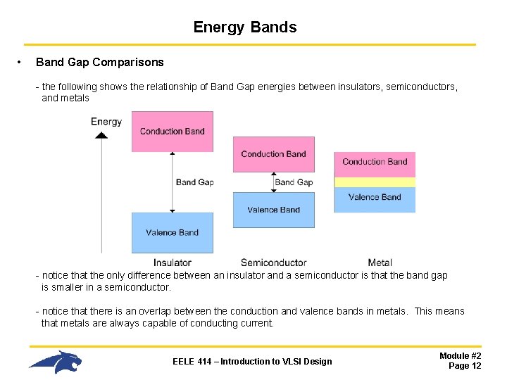
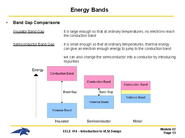
Energy Bands • Band Gap Comparisons - the following shows the relationship of Band Gap energies between insulators, semiconductors, and metals - notice that the only difference between an insulator and a semiconductor is that the band gap is smaller in a semiconductor. - notice that there is an overlap between the conduction and valence bands in metals. This means that metals are always capable of conducting current. EELE 414 – Introduction to VLSI Design Module #2 Page 12

Energy Bands • Band Gap Comparisons Insulator Band Gap : it is large enough so that at ordinary temperatures, no electrons reach the conduction band Semiconductor Band Gap : it is small enough so that at ordinary temperatures, thermal energy can give an electron enough energy to jump to the conduction band : we can also change the semiconductor into a conductor by introducing impurities EELE 414 – Introduction to VLSI Design Module #2 Page 13

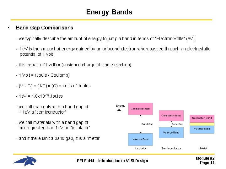
Energy Bands • Band Gap Comparisons - we typically describe the amount of energy to jump a band in terms of “Electron Volts” (e. V) - 1 e. V is the amount of energy gained by an unbound electron when passed through an electrostatic potential of 1 volt - it is equal to (1 volt) x (unsigned charge of single electron) - 1 Volt = (Joule / Coulomb) - (V x C) = (J/C) x (C) = units of Joules - 1 e. V = 1. 6 x 10 -19 Joules - we call materials with a band gap of ~ 1 e. V a “semiconductor” - we call materials with a band gap of much greater than 1 e. V an “insulator” - and if there isn’t a band gap, it is a “metal” EELE 414 – Introduction to VLSI Design Module #2 Page 14

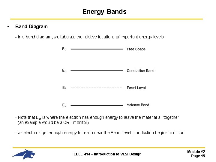
Energy Bands • Band Diagram - in a band diagram, we tabulate the relative locations of important energy levels - Note that EO is where the electron has enough energy to leave the material all together (an example would be a CRT monitor) - as electrons get enough energy to reach near the Fermi level, conduction begins to occur EELE 414 – Introduction to VLSI Design Module #2 Page 15

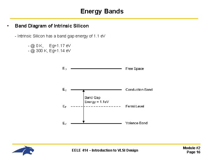
Energy Bands • Band Diagram of Intrinsic Silicon - Intrinsic Silicon has a band gap energy of 1. 1 e. V - @ 0 K, Eg=1. 17 e. V - @ 300 K, Eg=1. 14 e. V EELE 414 – Introduction to VLSI Design Module #2 Page 16

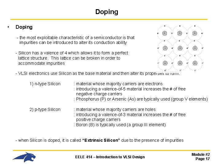
Doping • Doping - the most exploitable characteristic of a semiconductor is that impurities can be introduced to alter its conduction ability - Silicon has a valence of 4 which allows it to form a perfect lattice structure. This lattice can be broken in order to accommodate impurities - VLSI electronics use Silicon as the base material and then alter its properties to form: 1) n-type Silicon : material whose majority carriers are electrons : introducing a valence-of-5 material increases the # of free negative charge carriers : Phosphorus (P) or Arsenic (As) are typically used (group V elements) 2) p-type Silicon : material whose majority carriers are holes : introducing a valence-of-3 material increases the # of free positive charge carriers : Boron (B) is typically used (a group III element) - when Silicon is doped, it is called “Extrinsic Silicon” due to the presence of impurities EELE 414 – Introduction to VLSI Design Module #2 Page 17

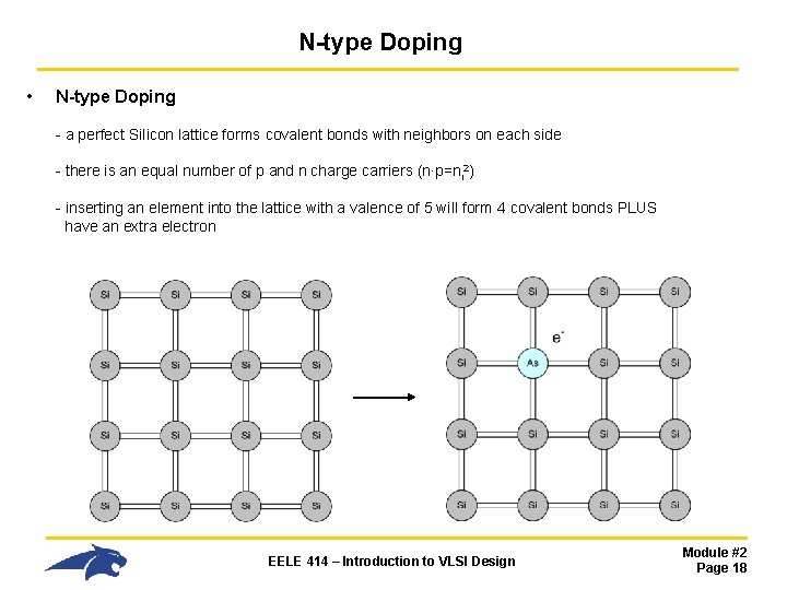
N-type Doping • N-type Doping - a perfect Silicon lattice forms covalent bonds with neighbors on each side - there is an equal number of p and n charge carriers (n∙p=ni 2) - inserting an element into the lattice with a valence of 5 will form 4 covalent bonds PLUS have an extra electron EELE 414 – Introduction to VLSI Design Module #2 Page 18

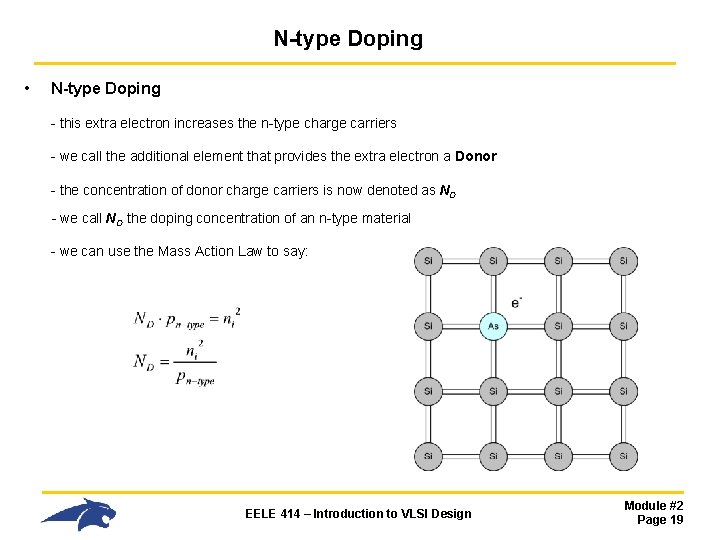
N-type Doping • N-type Doping - this extra electron increases the n-type charge carriers - we call the additional element that provides the extra electron a Donor - the concentration of donor charge carriers is now denoted as ND - we call ND the doping concentration of an n-type material - we can use the Mass Action Law to say: EELE 414 – Introduction to VLSI Design Module #2 Page 19

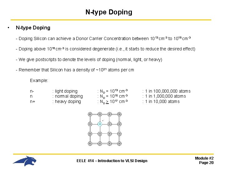
N-type Doping • N-type Doping - Doping Silicon can achieve a Donor Carrier Concentration between 1013 cm-3 to 1018 cm-3 - Doping above 1018 cm-3 is considered degenerate (i. e. , it starts to reduce the desired effect) - We give postscripts to denote the levels of doping (normal, light, or heavy) - Remember that Silicon has a density of ~1021 atoms per cm Example: nn n+ : light doping : normal doping : heavy doping : ND = 1013 cm-3 : ND = 1015 cm-3 : ND > 1017 cm-3 : 1 in 100, 000 atoms : 1 in 1, 000 atoms : 1 in 10, 000 atoms EELE 414 – Introduction to VLSI Design Module #2 Page 20

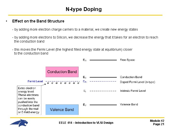
N-type Doping • Effect on the Band Structure - by adding more electron charge carriers to a material, we create new energy states - by adding more electrons to Silicon, we decrease the energy that it takes for an electron to reach the conduction band - this moves the Fermi Level (the highest filled energy state at equilibrium) closer to the conduction band EELE 414 – Introduction to VLSI Design Module #2 Page 21

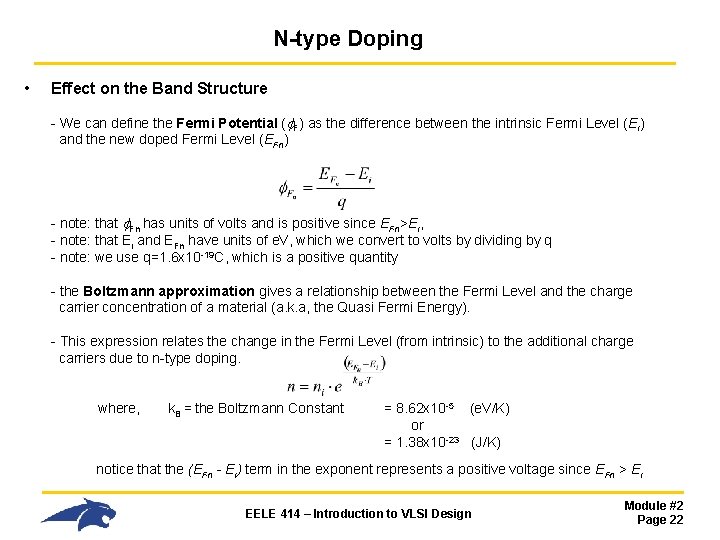
N-type Doping • Effect on the Band Structure - We can define the Fermi Potential ( F) as the difference between the intrinsic Fermi Level (Ei) and the new doped Fermi Level (EFn) - note: that Fn has units of volts and is positive since EFn>Ei, - note: that Ei and EFn have units of e. V, which we convert to volts by dividing by q - note: we use q=1. 6 x 10 -19 C, which is a positive quantity - the Boltzmann approximation gives a relationship between the Fermi Level and the charge carrier concentration of a material (a. k. a, the Quasi Fermi Energy). - This expression relates the change in the Fermi Level (from intrinsic) to the additional charge carriers due to n-type doping. where, k. B = the Boltzmann Constant = 8. 62 x 10 -5 (e. V/K) or = 1. 38 x 10 -23 (J/K) notice that the (EFn - Ei) term in the exponent represents a positive voltage since EFn > Ei EELE 414 – Introduction to VLSI Design Module #2 Page 22

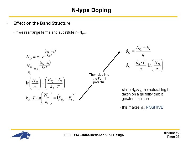
N-type Doping • Effect on the Band Structure - if we rearrange terms and substitute n=ND… Then plug into the Fermi potential - since ND>ni, the natural log is taken on a quantity that is greater than one - this makes Fn POSITIVE EELE 414 – Introduction to VLSI Design Module #2 Page 23

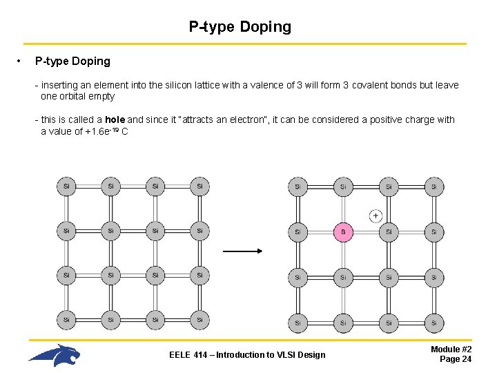
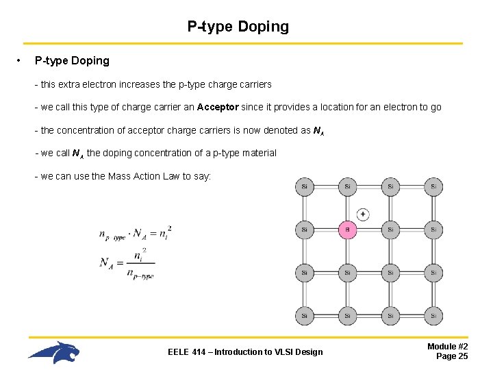
P-type Doping • P-type Doping - inserting an element into the silicon lattice with a valence of 3 will form 3 covalent bonds but leave one orbital empty - this is called a hole and since it “attracts an electron”, it can be considered a positive charge with a value of +1. 6 e-19 C EELE 414 – Introduction to VLSI Design Module #2 Page 24

P-type Doping • P-type Doping - this extra electron increases the p-type charge carriers - we call this type of charge carrier an Acceptor since it provides a location for an electron to go - the concentration of acceptor charge carriers is now denoted as NA - we call NA the doping concentration of a p-type material - we can use the Mass Action Law to say: EELE 414 – Introduction to VLSI Design Module #2 Page 25

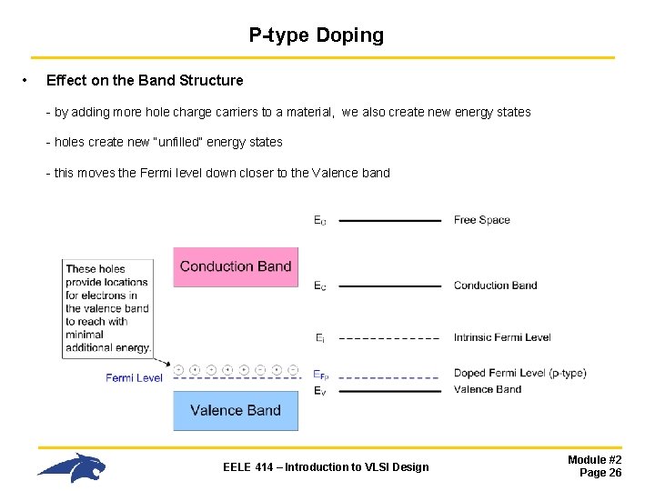
P-type Doping • Effect on the Band Structure - by adding more hole charge carriers to a material, we also create new energy states - holes create new “unfilled” energy states - this moves the Fermi level down closer to the Valence band EELE 414 – Introduction to VLSI Design Module #2 Page 26

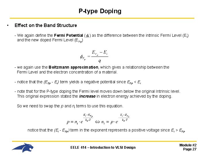
P-type Doping • Effect on the Band Structure - We again define the Fermi Potential ( F) as the difference between the intrinsic Fermi Level (Ei) and the new doped Fermi Level (EFp) - we again use the Boltzmann approximation, which gives a relationship between the Fermi Level and the electron concentration of a material. - notice that the (EFp - Ei) term yields a negative potential since EFp < Ei - note that for the P-type doping the Fermi level moves down below the original Intrinsic level. This original expression stated the increase in electron energy achieved by the doping. So we need to swap the p and ni terms to use this equation. notice that the (Ei - EFp) term in the exponent represents a positive voltage since Ei > EFp EELE 414 – Introduction to VLSI Design Module #2 Page 27

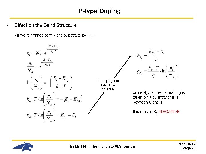
P-type Doping • Effect on the Band Structure - if we rearrange terms and substitute p=NA… Then plug into the Fermi potential - since NA>ni, the natural log is taken on a quantity that is between 0 and 1 - this makes Fp NEGATIVE EELE 414 – Introduction to VLSI Design Module #2 Page 28

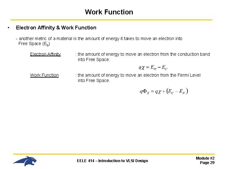
Work Function • Electron Affinity & Work Function - another metric of a material is the amount of energy it takes to move an electron into Free Space (E 0) Electron Affinity : the amount of energy to move an electron from the conduction band into Free Space. Work Function : the amount of energy to move an electron from the Fermi Level into Free Space. EELE 414 – Introduction to VLSI Design Module #2 Page 29

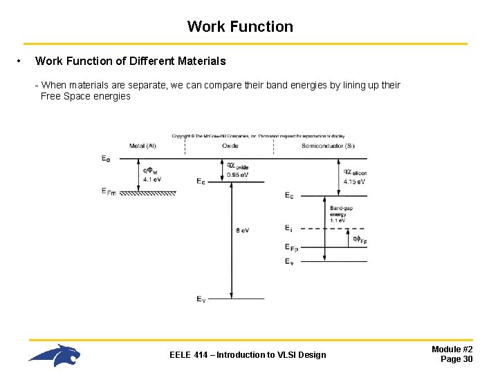
Work Function • Work Function of Different Materials - When materials are separate, we can compare their band energies by lining up their Free Space energies EELE 414 – Introduction to VLSI Design Module #2 Page 30

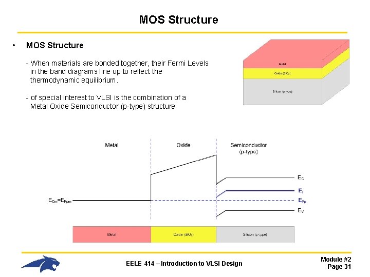
MOS Structure • MOS Structure - When materials are bonded together, their Fermi Levels in the band diagrams line up to reflect thermodynamic equilibrium. - of special interest to VLSI is the combination of a Metal Oxide Semiconductor (p-type) structure EELE 414 – Introduction to VLSI Design Module #2 Page 31

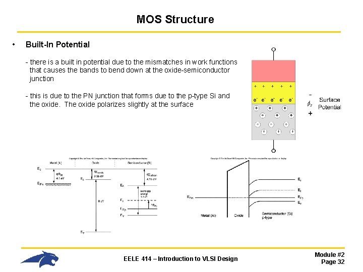
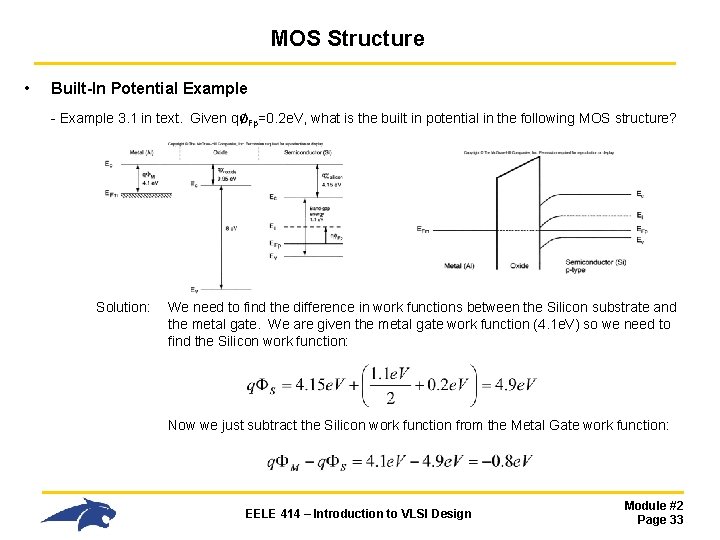
MOS Structure • Built-In Potential - there is a built in potential due to the mismatches in work functions that causes the bands to bend down at the oxide-semiconductor junction - this is due to the PN junction that forms due to the p-type Si and the oxide. The oxide polarizes slightly at the surface EELE 414 – Introduction to VLSI Design Module #2 Page 32

MOS Structure • Built-In Potential Example - Example 3. 1 in text. Given q∅Fp=0. 2 e. V, what is the built in potential in the following MOS structure? Solution: We need to find the difference in work functions between the Silicon substrate and the metal gate. We are given the metal gate work function (4. 1 e. V) so we need to find the Silicon work function: Now we just subtract the Silicon work function from the Metal Gate work function: EELE 414 – Introduction to VLSI Design Module #2 Page 33

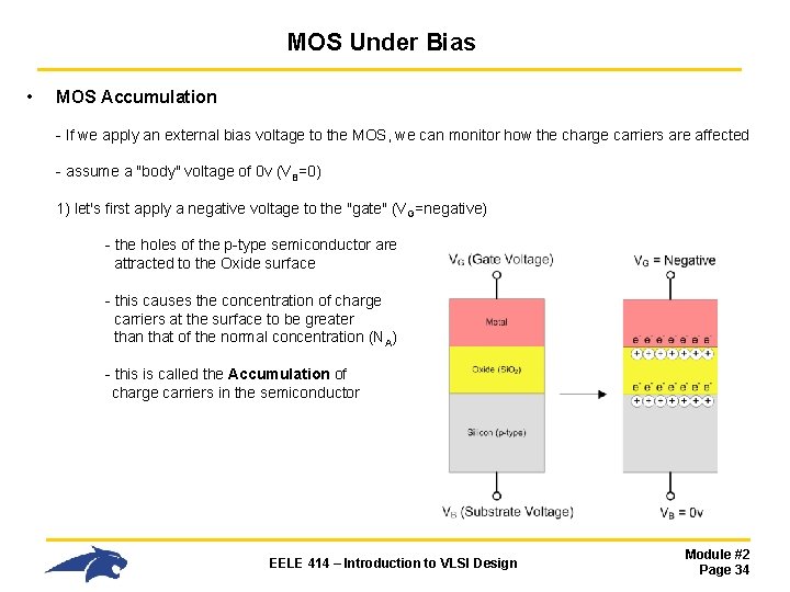
MOS Under Bias • MOS Accumulation - If we apply an external bias voltage to the MOS, we can monitor how the charge carriers are affected - assume a "body" voltage of 0 v (VB=0) 1) let's first apply a negative voltage to the "gate" (VG=negative) - the holes of the p-type semiconductor are attracted to the Oxide surface - this causes the concentration of charge carriers at the surface to be greater than that of the normal concentration (NA) - this is called the Accumulation of charge carriers in the semiconductor EELE 414 – Introduction to VLSI Design Module #2 Page 34

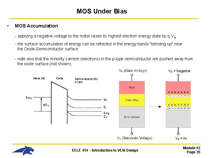
MOS Under Bias • MOS Accumulation - applying a negative voltage to the metal raises its highest electron energy state by q·VG - the surface accumulation of energy can be reflected in the energy bands "bending up" near the Oxide-Semiconductor surface - note also that the minority carriers (electrons) in the p-type semiconductor are pushed away from the oxide surface (not shown) EELE 414 – Introduction to VLSI Design Module #2 Page 35

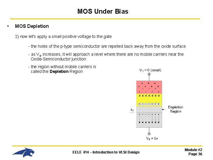
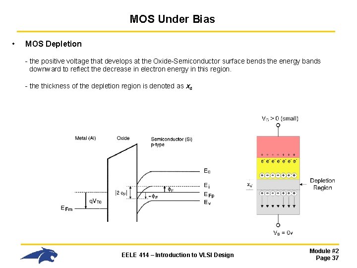
MOS Under Bias • MOS Depletion 2) now let's apply a small positive voltage to the gate - the holes of the p-type semiconductor are repelled back away from the oxide surface - as VG increases, it will approach a level where there are no mobile carriers near the Oxide-Semiconductor junction - the region without mobile carriers is called the Depletion Region EELE 414 – Introduction to VLSI Design Module #2 Page 36

MOS Under Bias • MOS Depletion - the positive voltage that develops at the Oxide-Semiconductor surface bends the energy bands downward to reflect the decrease in electron energy in this region. - the thickness of the depletion region is denoted as xd EELE 414 – Introduction to VLSI Design Module #2 Page 37

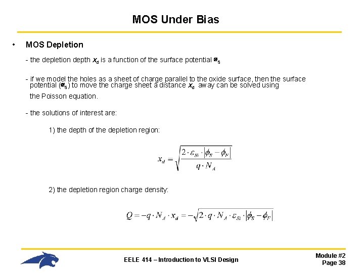
MOS Under Bias • MOS Depletion - the depletion depth xd is a function of the surface potential ∅S - if we model the holes as a sheet of charge parallel to the oxide surface, then the surface potential (∅S) to move the charge sheet a distance xd away can be solved using the Poisson equation. - the solutions of interest are: 1) the depth of the depletion region: 2) the depletion region charge density: EELE 414 – Introduction to VLSI Design Module #2 Page 38

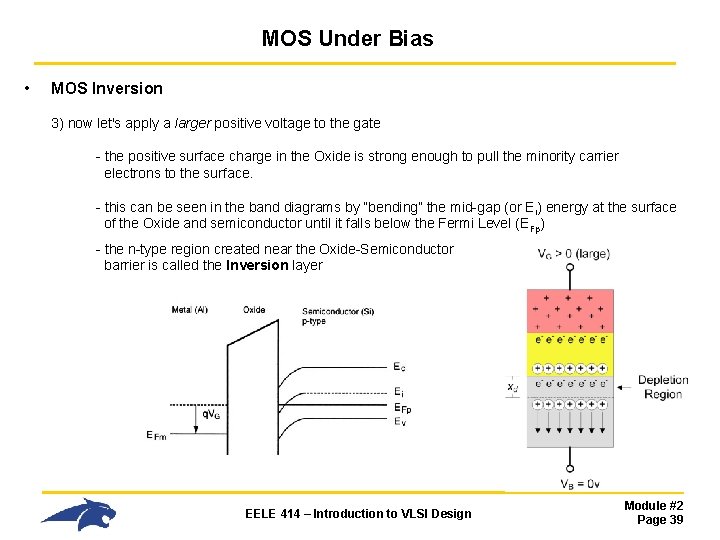
MOS Under Bias • MOS Inversion 3) now let's apply a larger positive voltage to the gate - the positive surface charge in the Oxide is strong enough to pull the minority carrier electrons to the surface. - this can be seen in the band diagrams by “bending” the mid-gap (or Ei) energy at the surface of the Oxide and semiconductor until it falls below the Fermi Level (EFp) - the n-type region created near the Oxide-Semiconductor barrier is called the Inversion layer EELE 414 – Introduction to VLSI Design Module #2 Page 39

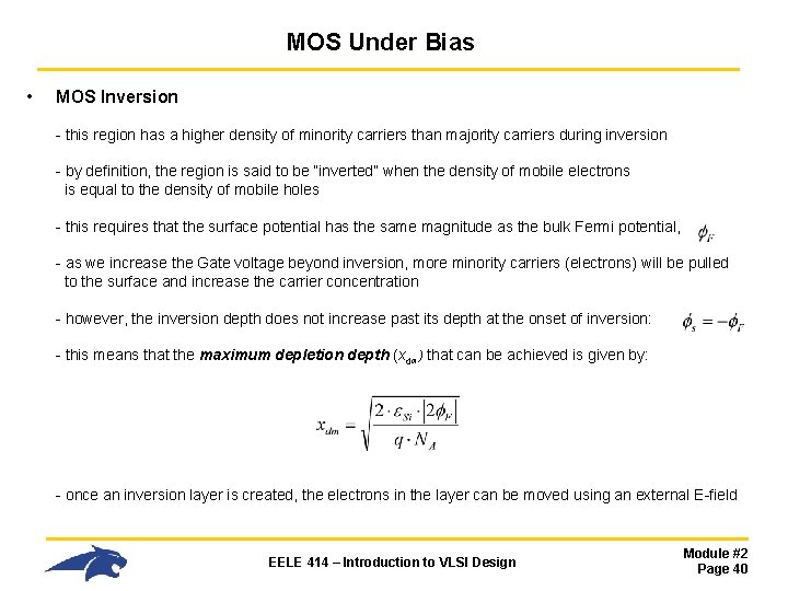
MOS Under Bias • MOS Inversion - this region has a higher density of minority carriers than majority carriers during inversion - by definition, the region is said to be “inverted” when the density of mobile electrons is equal to the density of mobile holes - this requires that the surface potential has the same magnitude as the bulk Fermi potential, - as we increase the Gate voltage beyond inversion, more minority carriers (electrons) will be pulled to the surface and increase the carrier concentration - however, the inversion depth does not increase past its depth at the onset of inversion: - this means that the maximum depletion depth (xdm) that can be achieved is given by: - once an inversion layer is created, the electrons in the layer can be moved using an external E-field EELE 414 – Introduction to VLSI Design Module #2 Page 40

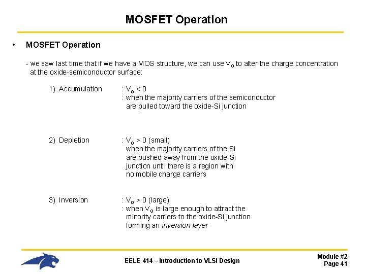
MOSFET Operation • MOSFET Operation - we saw last time that if we have a MOS structure, we can use VG to alter the charge concentration at the oxide-semiconductor surface: 1) Accumulation : VG < 0 : when the majority carriers of the semiconductor are pulled toward the oxide-Si junction 2) Depletion : VG > 0 (small) when the majority carriers of the Si are pushed away from the oxide-Si junction until there is a region with no mobile charge carriers 3) Inversion : VG > 0 (large) : when VG is large enough to attract the minority carriers to the oxide-Si junction forming an inversion layer EELE 414 – Introduction to VLSI Design Module #2 Page 41

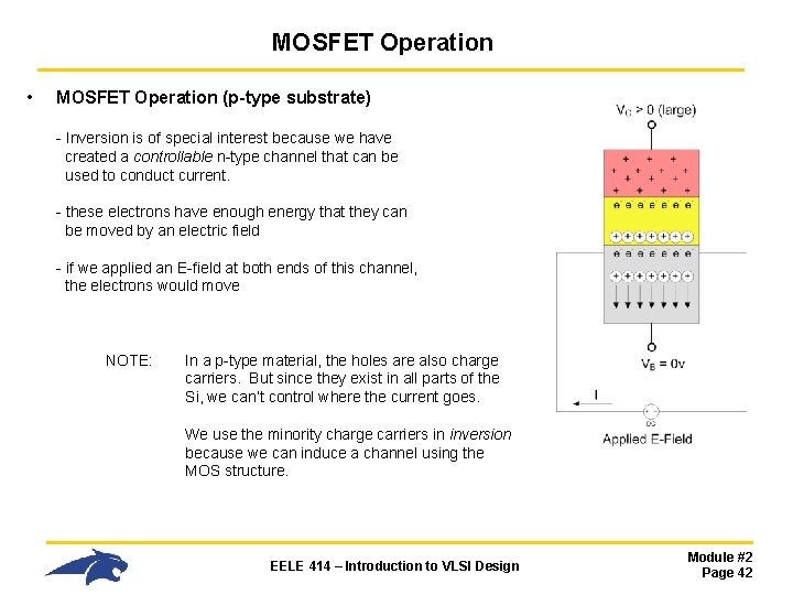
MOSFET Operation • MOSFET Operation (p-type substrate) - Inversion is of special interest because we have created a controllable n-type channel that can be used to conduct current. - these electrons have enough energy that they can be moved by an electric field - if we applied an E-field at both ends of this channel, the electrons would move NOTE: In a p-type material, the holes are also charge carriers. But since they exist in all parts of the Si, we can’t control where the current goes. We use the minority charge carriers in inversion because we can induce a channel using the MOS structure. EELE 414 – Introduction to VLSI Design Module #2 Page 42

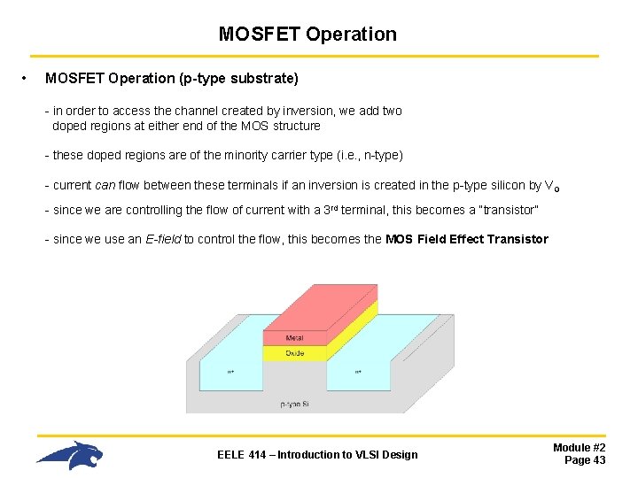
MOSFET Operation • MOSFET Operation (p-type substrate) - in order to access the channel created by inversion, we add two doped regions at either end of the MOS structure - these doped regions are of the minority carrier type (i. e. , n-type) - current can flow between these terminals if an inversion is created in the p-type silicon by VG - since we are controlling the flow of current with a 3 rd terminal, this becomes a “transistor” - since we use an E-field to control the flow, this becomes the MOS Field Effect Transistor EELE 414 – Introduction to VLSI Design Module #2 Page 43

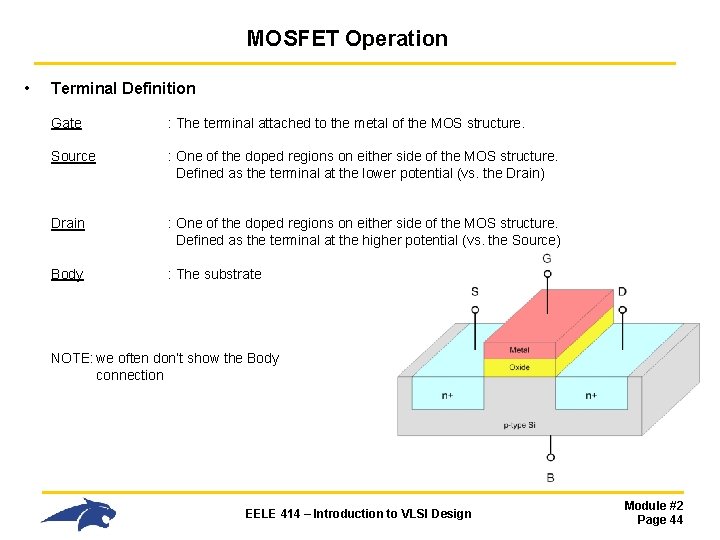
MOSFET Operation • Terminal Definition Gate : The terminal attached to the metal of the MOS structure. Source : One of the doped regions on either side of the MOS structure. Defined as the terminal at the lower potential (vs. the Drain) Drain : One of the doped regions on either side of the MOS structure. Defined as the terminal at the higher potential (vs. the Source) Body : The substrate NOTE: we often don’t show the Body connection EELE 414 – Introduction to VLSI Design Module #2 Page 44

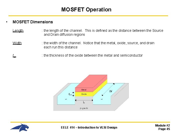
MOSFET Operation • MOSFET Dimensions Length : the length of the channel. This is defined as the distance between the Source and Drain diffusion regions Width : the width of the channel. Notice that the metal, oxide, source, and drain each run this distance tox : the thickness of the oxide between the metal and semiconductor EELE 414 – Introduction to VLSI Design Module #2 Page 45

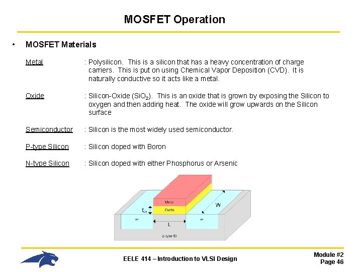
MOSFET Operation • MOSFET Materials Metal : Polysilicon. This is a silicon that has a heavy concentration of charge carriers. This is put on using Chemical Vapor Deposition (CVD). It is naturally conductive so it acts like a metal. Oxide : Silicon-Oxide (Si. O 2). This is an oxide that is grown by exposing the Silicon to oxygen and then adding heat. The oxide will grow upwards on the Silicon surface Semiconductor : Silicon is the most widely used semiconductor. P-type Silicon : Silicon doped with Boron N-type Silicon : Silicon doped with either Phosphorus or Arsenic EELE 414 – Introduction to VLSI Design Module #2 Page 46

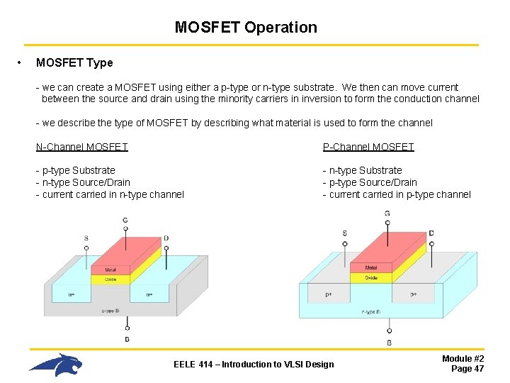
MOSFET Operation • MOSFET Type - we can create a MOSFET using either a p-type or n-type substrate. We then can move current between the source and drain using the minority carriers in inversion to form the conduction channel - we describe the type of MOSFET by describing what material is used to form the channel N-Channel MOSFET P-Channel MOSFET - p-type Substrate - n-type Source/Drain - current carried in n-type channel - n-type Substrate - p-type Source/Drain - current carried in p-type channel EELE 414 – Introduction to VLSI Design Module #2 Page 47

MOSFET Operation • Enhancement vs. Depletion MOSFETS Enhancement Type : when a MOSFET has no conduction channel at VG=0 v : also called enhancement-mode : we apply a voltage at the gate to turn ON the channel : this is used most frequently and what we will use to learn VLSI Depletion Type : when a MOSFET does have a conducting channel at VG=0 v : also called depletion-mode : we apply a voltage at the gate to turn OFF the channel : we won’t use this type of transistor for now Note: We will learn VLSI circuits using enhancement-type, n-channel MOSFETS. All of the principles apply directly to Depletion-type MOSFETs as well as p-channel MOSFETs. EELE 414 – Introduction to VLSI Design Module #2 Page 48

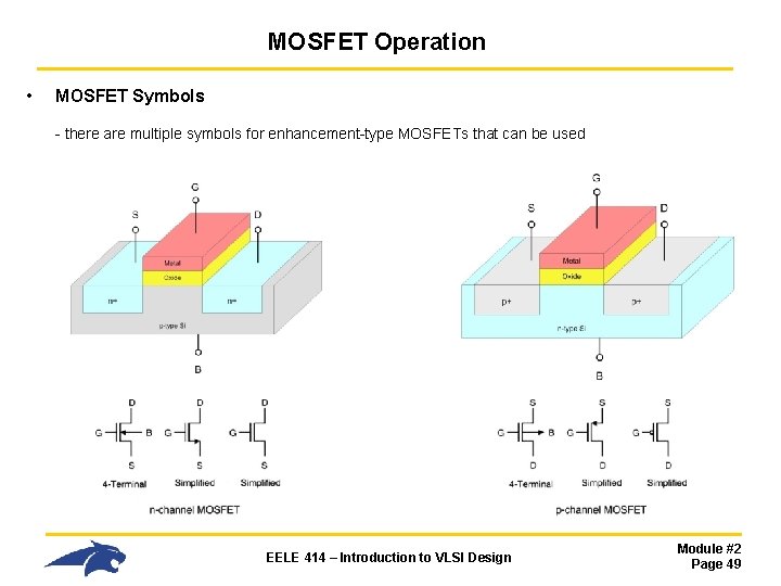
MOSFET Operation • MOSFET Symbols - there are multiple symbols for enhancement-type MOSFETs that can be used EELE 414 – Introduction to VLSI Design Module #2 Page 49

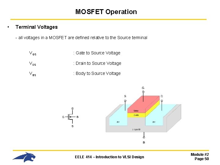
MOSFET Operation • Terminal Voltages - all voltages in a MOSFET are defined relative to the Source terminal VGS : Gate to Source Voltage VDS : Drain to Source Voltage VBS : Body to Source Voltage EELE 414 – Introduction to VLSI Design Module #2 Page 50

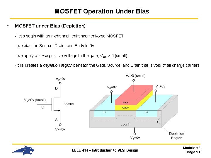
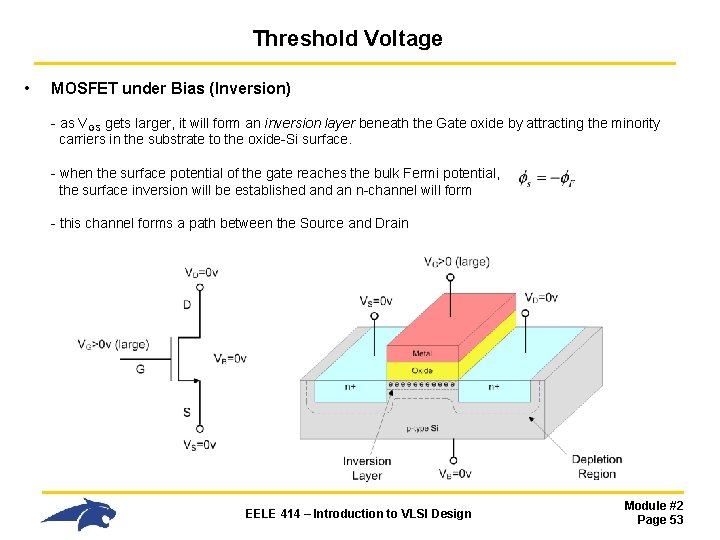
MOSFET Operation Under Bias • MOSFET under Bias (Depletion) - let’s begin with an n-channel, enhancement-type MOSFET - we bias the Source, Drain, and Body to 0 v - we apply a small positive voltage to the gate, VGS > 0 (small) - this creates a depletion region beneath the Gate, Source, and Drain that is void of all charge carriers EELE 414 – Introduction to VLSI Design Module #2 Page 51

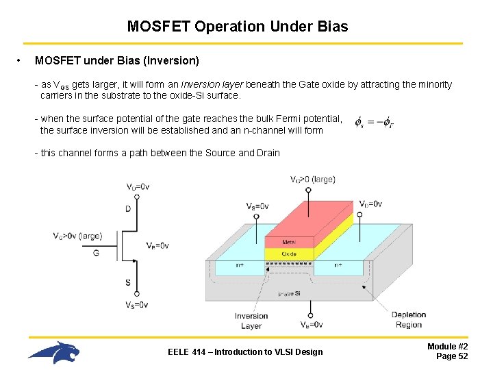
MOSFET Operation Under Bias • MOSFET under Bias (Inversion) - as VGS gets larger, it will form an inversion layer beneath the Gate oxide by attracting the minority carriers in the substrate to the oxide-Si surface. - when the surface potential of the gate reaches the bulk Fermi potential, the surface inversion will be established an n-channel will form - this channel forms a path between the Source and Drain EELE 414 – Introduction to VLSI Design Module #2 Page 52

Threshold Voltage • MOSFET under Bias (Inversion) - as VGS gets larger, it will form an inversion layer beneath the Gate oxide by attracting the minority carriers in the substrate to the oxide-Si surface. - when the surface potential of the gate reaches the bulk Fermi potential, the surface inversion will be established an n-channel will form - this channel forms a path between the Source and Drain EELE 414 – Introduction to VLSI Design Module #2 Page 53

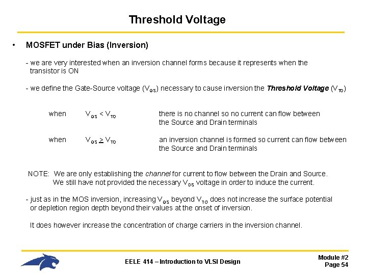
Threshold Voltage • MOSFET under Bias (Inversion) - we are very interested when an inversion channel forms because it represents when the transistor is ON - we define the Gate-Source voltage (VGS) necessary to cause inversion the Threshold Voltage (VT 0) when VGS < VT 0 there is no channel so no current can flow between the Source and Drain terminals when VGS > VT 0 an inversion channel is formed so current can flow between the Source and Drain terminals NOTE: We are only establishing the channel for current to flow between the Drain and Source. We still have not provided the necessary VDS voltage in order to induce the current. - just as in the MOS inversion, increasing VGS beyond VTO does not increase the surface potential or depletion region depth beyond their values at the onset of inversion. It does however increase the concentration of charge carriers in the inversion channel. EELE 414 – Introduction to VLSI Design Module #2 Page 54

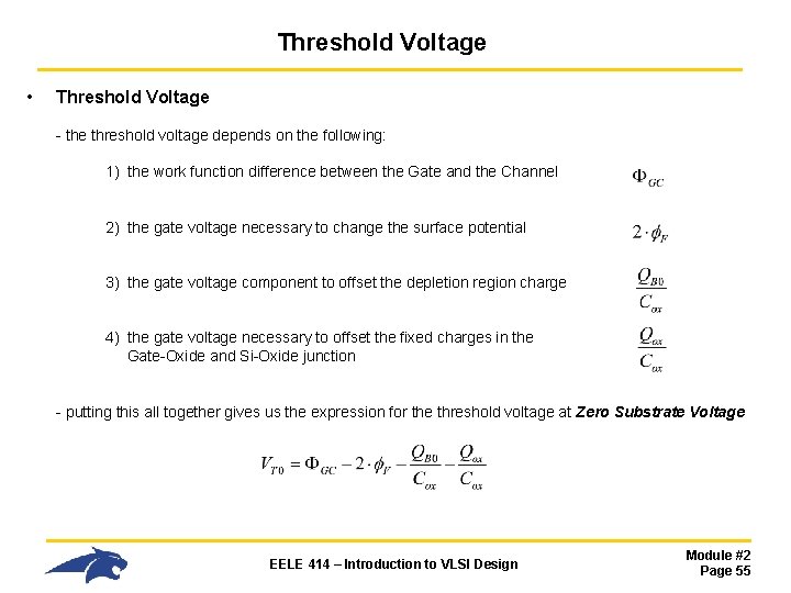
Threshold Voltage • Threshold Voltage - the threshold voltage depends on the following: 1) the work function difference between the Gate and the Channel 2) the gate voltage necessary to change the surface potential 3) the gate voltage component to offset the depletion region charge 4) the gate voltage necessary to offset the fixed charges in the Gate-Oxide and Si-Oxide junction - putting this all together gives us the expression for the threshold voltage at Zero Substrate Voltage EELE 414 – Introduction to VLSI Design Module #2 Page 55

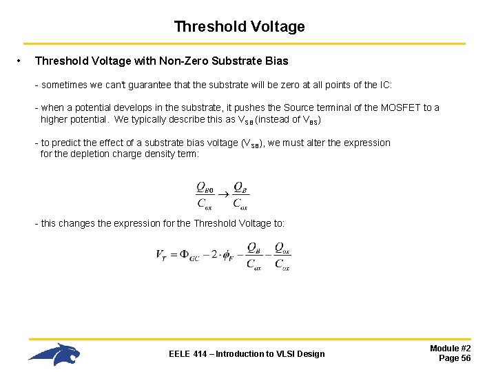
Threshold Voltage • Threshold Voltage with Non-Zero Substrate Bias - sometimes we can't guarantee that the substrate will be zero at all points of the IC: - when a potential develops in the substrate, it pushes the Source terminal of the MOSFET to a higher potential. We typically describe this as VSB (instead of VBS) - to predict the effect of a substrate bias voltage (VSB), we must alter the expression for the depletion charge density term: - this changes the expression for the Threshold Voltage to: EELE 414 – Introduction to VLSI Design Module #2 Page 56

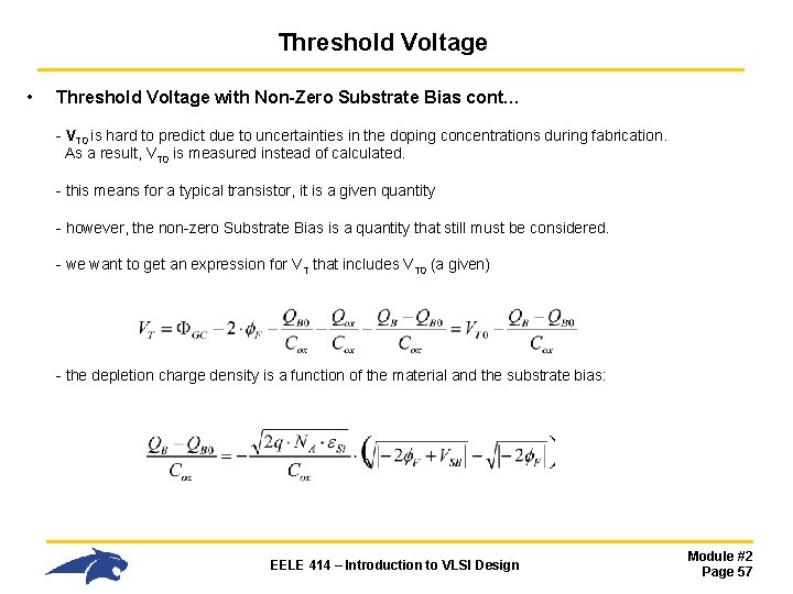
Threshold Voltage • Threshold Voltage with Non-Zero Substrate Bias cont… - VT 0 is hard to predict due to uncertainties in the doping concentrations during fabrication. As a result, VT 0 is measured instead of calculated. - this means for a typical transistor, it is a given quantity - however, the non-zero Substrate Bias is a quantity that still must be considered. - we want to get an expression for VT that includes VT 0 (a given) - the depletion charge density is a function of the material and the substrate bias: EELE 414 – Introduction to VLSI Design Module #2 Page 57

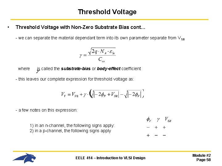
Threshold Voltage • Threshold Voltage with Non-Zero Substrate Bias cont… - we can separate the material dependant term into its own parameter separate from VSB where is called the substrate-bias or body-effect coefficient - this leaves our complete expression for threshold voltage as: - a few notes on this expression: 1) in an n-channel, the following signs apply: 2) in a p-channel, the following signs apply EELE 414 – Introduction to VLSI Design Module #2 Page 58

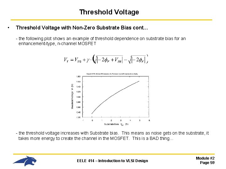
Threshold Voltage • Threshold Voltage with Non-Zero Substrate Bias cont… - the following plot shows an example of threshold dependence on substrate bias for an enhancement-type, n-channel MOSFET - the threshold voltage increases with Substrate bias. This means as noise gets on the substrate, it takes more energy to create the channel in the MOSFET. This is a BAD thing… EELE 414 – Introduction to VLSI Design Module #2 Page 59

MOSFET I-V Characteristics • MOSFET I-V Characteristics - we have seen how the Gate-to-Source voltage (VGS) induces a channel between the Source and Drain for current to flow through - this current is denoted IDS - remember that this current doesn't flow unless a potential exists between VD and VS - the voltage that controls the current flow is denoted as VDS - once again, we start by applying a small voltage and watching how IDS responds - notice that now we actually have two control variables that effect the current flow, VGS and VDS - this is typical operating behavior for a 3 -terminal device or transistor - we can use an enhancement n-channel MOSFET to understand the IV characteristics and then directly apply them to p-channel and depletion-type devices EELE 414 – Introduction to VLSI Design Module #2 Page 60

MOSFET I-V Characteristics • MOSFET I-V Characteristics : Cutoff Region - when VGS < VT, there is no channel formed between the Drain and Source and hence IDS=0 A - this region is called the Cutoff Region - this region of operation is when the Transistor is OFF EELE 414 – Introduction to VLSI Design Module #2 Page 61

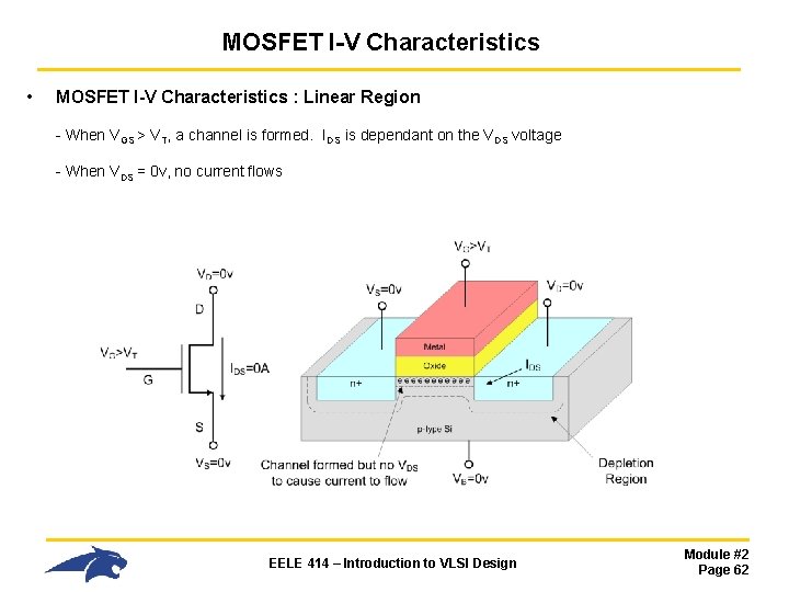
MOSFET I-V Characteristics • MOSFET I-V Characteristics : Linear Region - When VGS > VT, a channel is formed. IDS is dependant on the VDS voltage - When VDS = 0 v, no current flows EELE 414 – Introduction to VLSI Design Module #2 Page 62

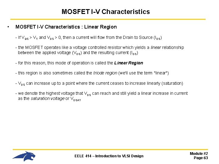
MOSFET I-V Characteristics • MOSFET I-V Characteristics : Linear Region - If VGS > VT and VDS > 0, then a current will flow from the Drain to Source (IDS) - the MOSFET operates like a voltage controlled resistor which yields a linear relationship between the applied voltage (VDS) and the resulting current (IDS) - for this reason, this mode of operation is called the Linear Region - this region is also sometimes called the triode region (we'll use the term "linear") - VDS can increase up to a point where the current ceases to increase linearly (saturation) - we denote the highest voltage that VDS can reach and still yield a linear increase in current as the saturation voltage or VDSAT EELE 414 – Introduction to VLSI Design Module #2 Page 63

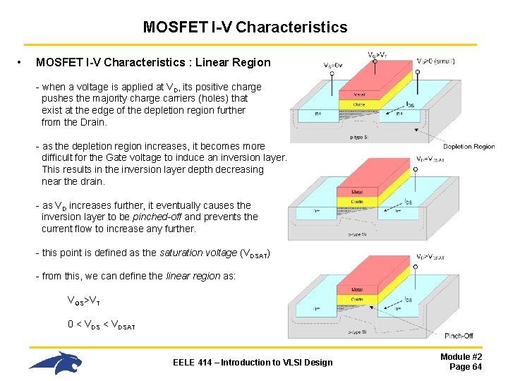
MOSFET I-V Characteristics • MOSFET I-V Characteristics : Linear Region - when a voltage is applied at VD, its positive charge pushes the majority charge carriers (holes) that exist at the edge of the depletion region further from the Drain. - as the depletion region increases, it becomes more difficult for the Gate voltage to induce an inversion layer. This results in the inversion layer depth decreasing near the drain. - as VD increases further, it eventually causes the inversion layer to be pinched-off and prevents the current flow to increase any further. - this point is defined as the saturation voltage (VDSAT) - from this, we can define the linear region as: VGS>VT 0 < VDSAT EELE 414 – Introduction to VLSI Design Module #2 Page 64

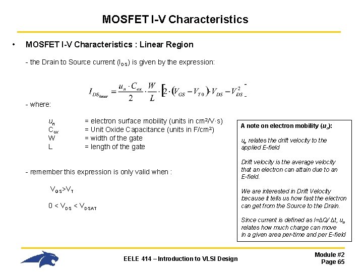
MOSFET I-V Characteristics • MOSFET I-V Characteristics : Linear Region - the Drain to Source current (IDS) is given by the expression: - where: un Cox W L = electron surface mobility (units in cm 2/V·s) = Unit Oxide Capacitance (units in F/cm 2) = width of the gate = length of the gate - remember this expression is only valid when : VGS>VT A note on electron mobility (un): un relates the drift velocity to the applied E-field Drift velocity is the average velocity that an electron can attain due to an E-field. We are interested in Drift Velocity because it tells us how fast the electron can get from the Source to the Drain. 0 < VDSAT Since current is defined as I=∆Q/ ∆t, un relates how much charge can move in a given area per-time and per E-field EELE 414 – Introduction to VLSI Design Module #2 Page 65

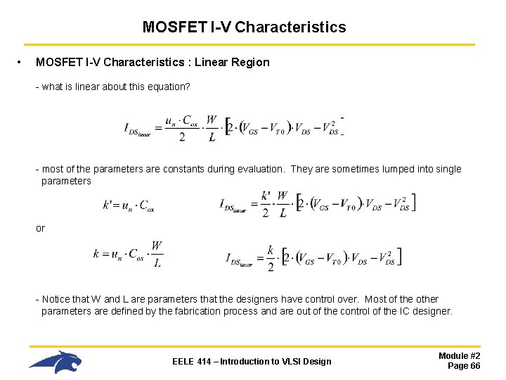
MOSFET I-V Characteristics • MOSFET I-V Characteristics : Linear Region - what is linear about this equation? - most of the parameters are constants during evaluation. They are sometimes lumped into single parameters or - Notice that W and L are parameters that the designers have control over. Most of the other parameters are defined by the fabrication process and are out of the control of the IC designer. EELE 414 – Introduction to VLSI Design Module #2 Page 66

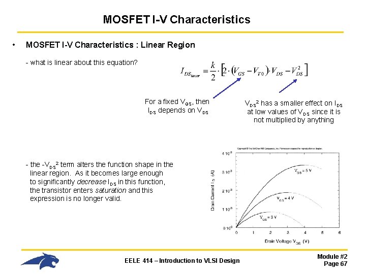
MOSFET I-V Characteristics • MOSFET I-V Characteristics : Linear Region - what is linear about this equation? For a fixed VGS, then IDS depends on VDS 2 has a smaller effect on IDS at low values of VDS since it is not multiplied by anything - the -VDS 2 term alters the function shape in the linear region. As it becomes large enough to significantly decrease IDS in this function, the transistor enters saturation and this expression is no longer valid. EELE 414 – Introduction to VLSI Design Module #2 Page 67

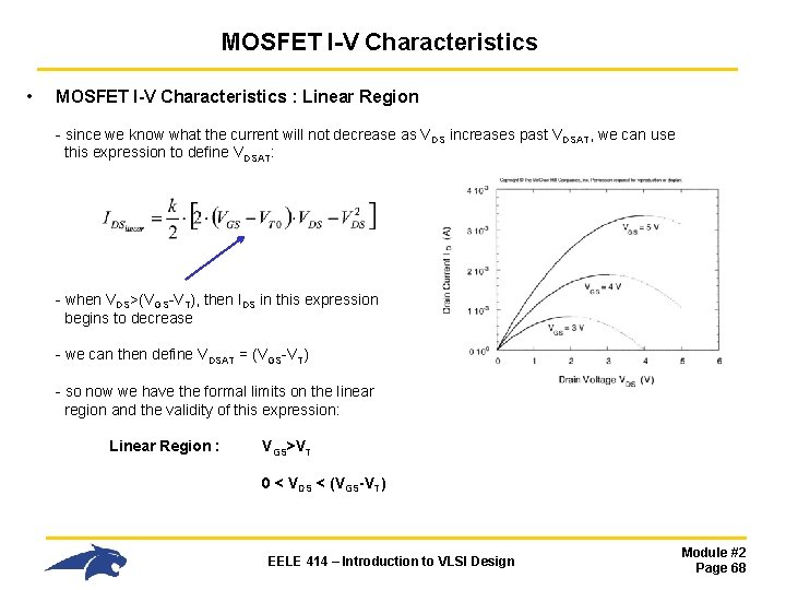
MOSFET I-V Characteristics • MOSFET I-V Characteristics : Linear Region - since we know what the current will not decrease as VDS increases past VDSAT, we can use this expression to define VDSAT: - when VDS>(VGS-VT), then IDS in this expression begins to decrease - we can then define VDSAT = (VGS-VT) - so now we have the formal limits on the linear region and the validity of this expression: Linear Region : VGS>VT 0 < VDS < (VGS-VT) EELE 414 – Introduction to VLSI Design Module #2 Page 68

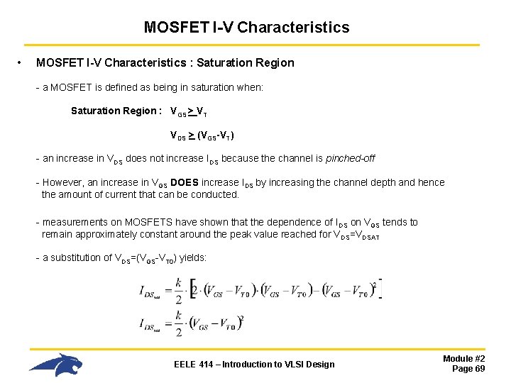
MOSFET I-V Characteristics • MOSFET I-V Characteristics : Saturation Region - a MOSFET is defined as being in saturation when: Saturation Region : VGS > VT VDS > (VGS-VT) - an increase in VDS does not increase IDS because the channel is pinched-off - However, an increase in VGS DOES increase IDS by increasing the channel depth and hence the amount of current that can be conducted. - measurements on MOSFETS have shown that the dependence of IDS on VGS tends to remain approximately constant around the peak value reached for VDS=VDSAT - a substitution of VDS=(VGS-VT 0) yields: EELE 414 – Introduction to VLSI Design Module #2 Page 69

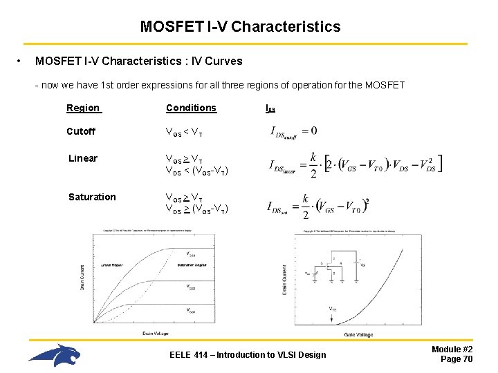
MOSFET I-V Characteristics • MOSFET I-V Characteristics : IV Curves - now we have 1 st order expressions for all three regions of operation for the MOSFET Region Conditions Cutoff VGS < VT Linear VGS > VT VDS < (VGS-VT) Saturation VGS > VT VDS > (VGS-VT) IDS EELE 414 – Introduction to VLSI Design Module #2 Page 70

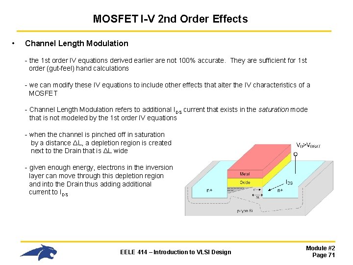
MOSFET I-V 2 nd Order Effects • Channel Length Modulation - the 1 st order IV equations derived earlier are not 100% accurate. They are sufficient for 1 st order (gut-feel) hand calculations - we can modify these IV equations to include other effects that alter the IV characteristics of a MOSFET - Channel Length Modulation refers to additional IDS current that exists in the saturation mode that is not modeled by the 1 st order IV equations - when the channel is pinched off in saturation by a distance ΔL, a depletion region is created next to the Drain that is ΔL wide - given enough energy, electrons in the inversion layer can move through this depletion region and into the Drain thus adding additional current to IDS EELE 414 – Introduction to VLSI Design Module #2 Page 71

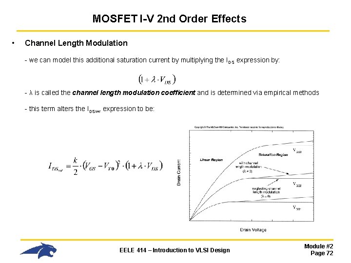
MOSFET I-V 2 nd Order Effects • Channel Length Modulation - we can model this additional saturation current by multiplying the IDS expression by: - λ is called the channel length modulation coefficient and is determined via empirical methods - this term alters the IDSSAT expression to be: EELE 414 – Introduction to VLSI Design Module #2 Page 72

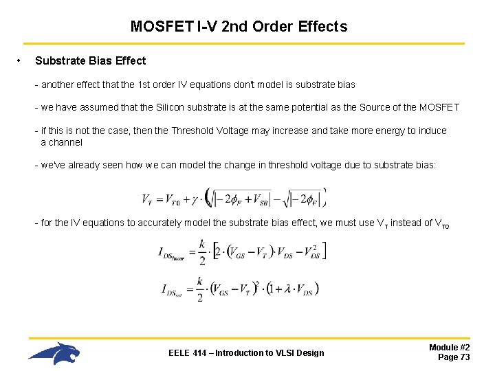
MOSFET I-V 2 nd Order Effects • Substrate Bias Effect - another effect that the 1 st order IV equations don't model is substrate bias - we have assumed that the Silicon substrate is at the same potential as the Source of the MOSFET - if this is not the case, then the Threshold Voltage may increase and take more energy to induce a channel - we've already seen how we can model the change in threshold voltage due to substrate bias: - for the IV equations to accurately model the substrate bias effect, we must use V T instead of VT 0 EELE 414 – Introduction to VLSI Design Module #2 Page 73

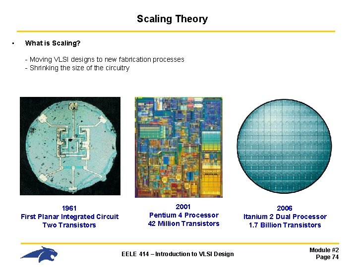
Scaling Theory • What is Scaling? - Moving VLSI designs to new fabrication processes - Shrinking the size of the circuitry 1961 First Planar Integrated Circuit Two Transistors 2001 Pentium 4 Processor 42 Million Transistors EELE 414 – Introduction to VLSI Design 2006 Itanium 2 Dual Processor 1. 7 Billion Transistors Module #2 Page 74

Scaling Theory • Why do we Scale? 1) Improve Performance • More complex systems 2) Increase Transistor Density • Reduce cost per transistor & size of system 300 mm wafer 3) Reduce Power • Smaller transistors require less supply voltage EELE 414 – Introduction to VLSI Design Module #2 Page 75

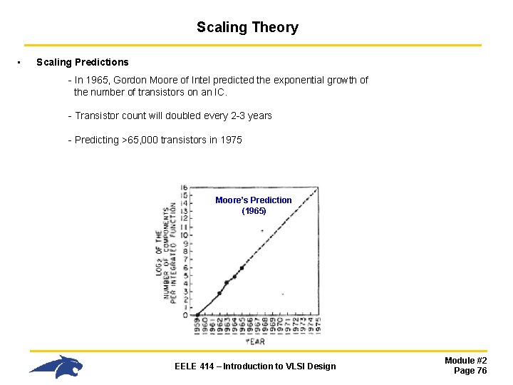
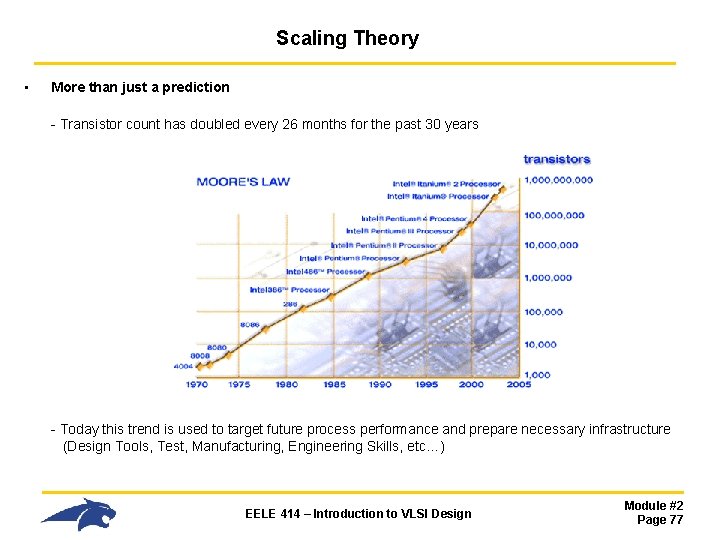
Scaling Theory • Scaling Predictions - In 1965, Gordon Moore of Intel predicted the exponential growth of the number of transistors on an IC. - Transistor count will doubled every 2 -3 years - Predicting >65, 000 transistors in 1975 Moore’s Prediction (1965) EELE 414 – Introduction to VLSI Design Module #2 Page 76

Scaling Theory • More than just a prediction - Transistor count has doubled every 26 months for the past 30 years - Today this trend is used to target future process performance and prepare necessary infrastructure (Design Tools, Test, Manufacturing, Engineering Skills, etc…) EELE 414 – Introduction to VLSI Design Module #2 Page 77

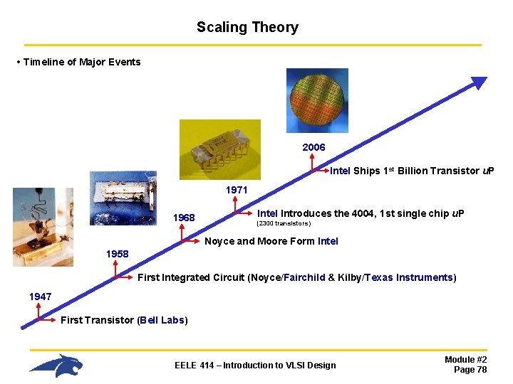
Scaling Theory • Timeline of Major Events 2006 Intel Ships 1 st Billion Transistor u. P 1971 1968 Intel Introduces the 4004, 1 st single chip u. P (2300 transistors) Noyce and Moore Form Intel 1958 First Integrated Circuit (Noyce/Fairchild & Kilby/Texas Instruments) 1947 First Transistor (Bell Labs) EELE 414 – Introduction to VLSI Design Module #2 Page 78

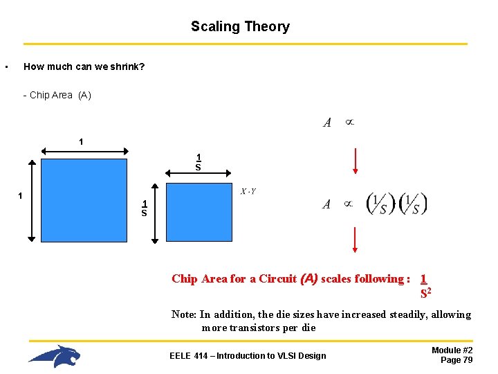
Scaling Theory • How much can we shrink? - Chip Area (A) 1 1 S Chip Area for a Circuit (A) scales following : 1 S 2 Note: In addition, the die sizes have increased steadily, allowing more transistors per die EELE 414 – Introduction to VLSI Design Module #2 Page 79

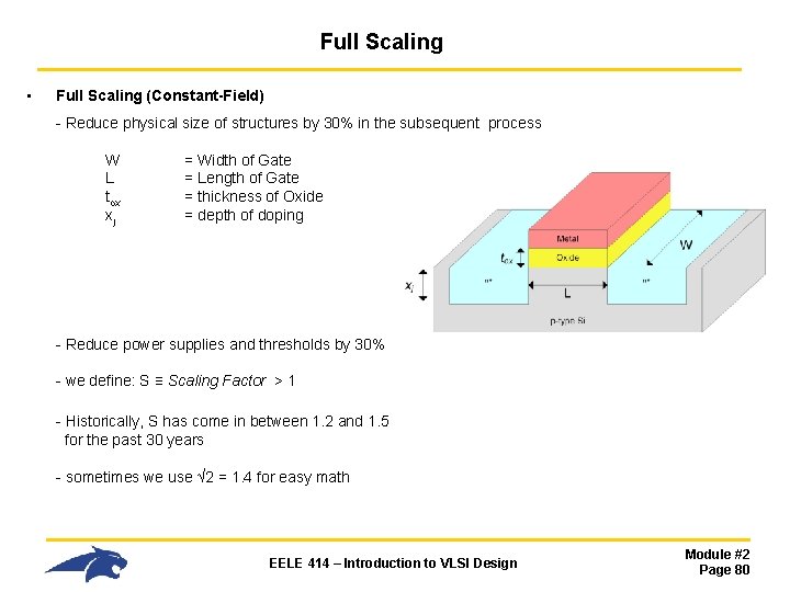
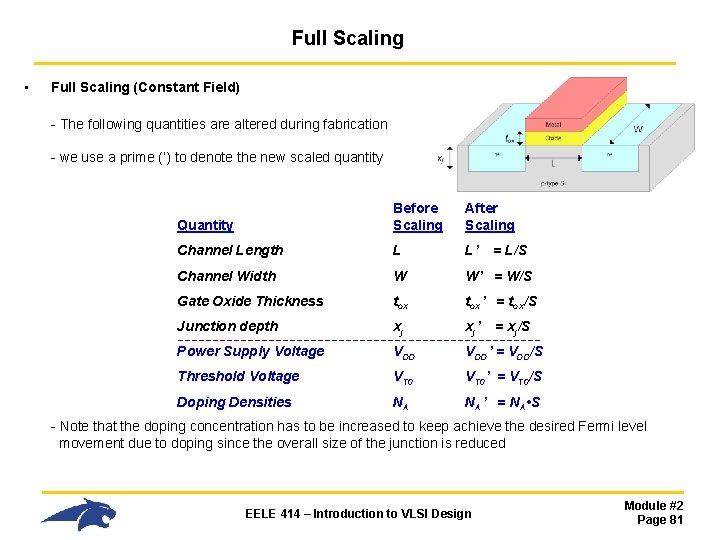
Full Scaling • Full Scaling (Constant-Field) - Reduce physical size of structures by 30% in the subsequent process W L tox xj = Width of Gate = Length of Gate = thickness of Oxide = depth of doping - Reduce power supplies and thresholds by 30% - we define: S ≡ Scaling Factor > 1 - Historically, S has come in between 1. 2 and 1. 5 for the past 30 years - sometimes we use √ 2 = 1. 4 for easy math EELE 414 – Introduction to VLSI Design Module #2 Page 80

Full Scaling • Full Scaling (Constant Field) - The following quantities are altered during fabrication - we use a prime (‘) to denote the new scaled quantity Quantity Before Scaling After Scaling Channel Length L L’ Channel Width W W’ = W/S Gate Oxide Thickness tox’ = tox/S Junction depth xj xj ’ Power Supply Voltage VDD’ = VDD/S Threshold Voltage VT 0’ = VT 0/S Doping Densities NA NA’ = NA • S = L/S = xj/S - Note that the doping concentration has to be increased to keep achieve the desired Fermi level movement due to doping since the overall size of the junction is reduced EELE 414 – Introduction to VLSI Design Module #2 Page 81

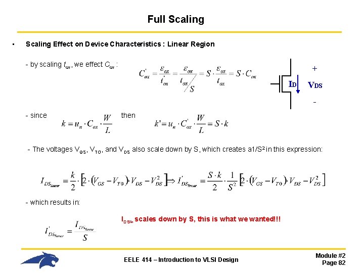
Full Scaling • Scaling Effect on Device Characteristics : Linear Region - by scaling tox, we effect Cox : + ID VDS - - since then - The voltages VGS, VTO, and VDS also scale down by S, which creates a 1/S 2 in this expression: - which results in: IDSlin scales down by S, this is what we wanted!!! EELE 414 – Introduction to VLSI Design Module #2 Page 82

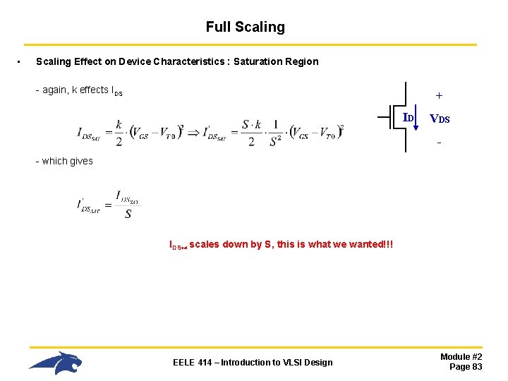
Full Scaling • Scaling Effect on Device Characteristics : Saturation Region - again, k effects IDS + ID VDS - - which gives IDSsat scales down by S, this is what we wanted!!! EELE 414 – Introduction to VLSI Design Module #2 Page 83

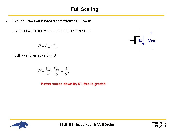
Full Scaling • Scaling Effect on Device Characteristics : Power - Static Power in the MOSFET can be described as: + ID VDS - - both quantities scale by 1/S Power scales down by S 2, this is great!!! EELE 414 – Introduction to VLSI Design Module #2 Page 84

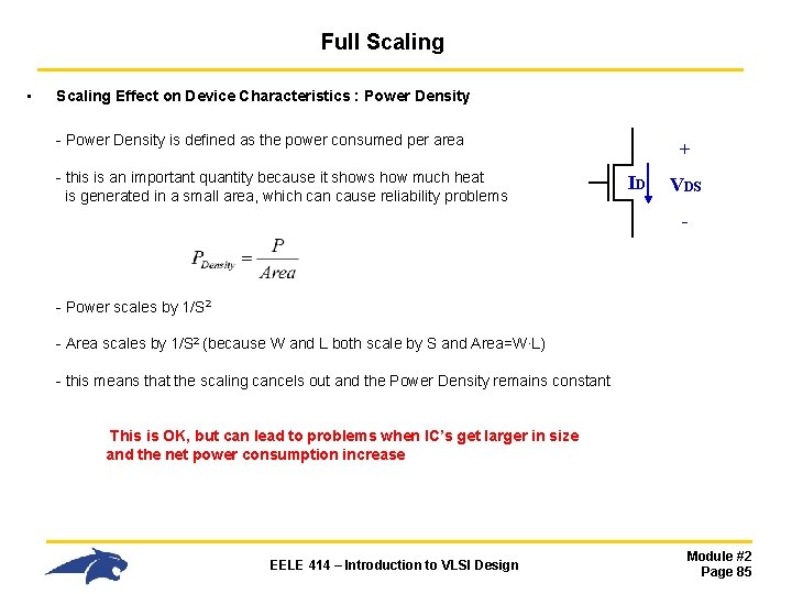
Full Scaling • Scaling Effect on Device Characteristics : Power Density - Power Density is defined as the power consumed per area - this is an important quantity because it shows how much heat is generated in a small area, which can cause reliability problems + ID VDS - - Power scales by 1/S 2 - Area scales by 1/S 2 (because W and L both scale by S and Area=W∙L) - this means that the scaling cancels out and the Power Density remains constant This is OK, but can lead to problems when IC’s get larger in size and the net power consumption increase EELE 414 – Introduction to VLSI Design Module #2 Page 85

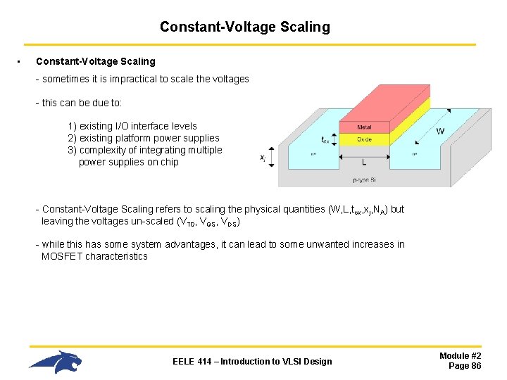
Constant-Voltage Scaling • Constant-Voltage Scaling - sometimes it is impractical to scale the voltages - this can be due to: 1) existing I/O interface levels 2) existing platform power supplies 3) complexity of integrating multiple power supplies on chip - Constant-Voltage Scaling refers to scaling the physical quantities (W, L, tox, xj, NA) but leaving the voltages un-scaled (VT 0, VGS, VDS) - while this has some system advantages, it can lead to some unwanted increases in MOSFET characteristics EELE 414 – Introduction to VLSI Design Module #2 Page 86

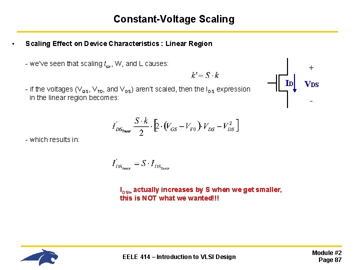
Constant-Voltage Scaling • Scaling Effect on Device Characteristics : Linear Region - we’ve seen that scaling tox, W, and L causes: - if the voltages (VGS, VT 0, and VDS) aren’t scaled, then the IDS expression in the linear region becomes: + ID VDS - - which results in: IDSlin actually increases by S when we get smaller, this is NOT what we wanted!!! EELE 414 – Introduction to VLSI Design Module #2 Page 87

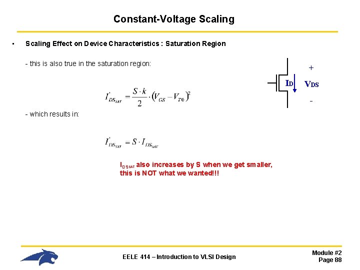
Constant-Voltage Scaling • Scaling Effect on Device Characteristics : Saturation Region - this is also true in the saturation region: + ID VDS - - which results in: IDSSAT also increases by S when we get smaller, this is NOT what we wanted!!! EELE 414 – Introduction to VLSI Design Module #2 Page 88

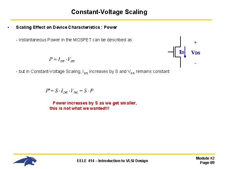
Constant-Voltage Scaling • Scaling Effect on Device Characteristics : Power - Instantaneous Power in the MOSFET can be described as: + ID VDS - - but in Constant-Voltage Scaling, IDS increases by S and VDS remains constant Power increases by S as we get smaller, this is not what we wanted!!! EELE 414 – Introduction to VLSI Design Module #2 Page 89

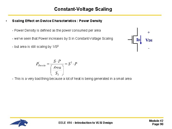
Constant-Voltage Scaling • Scaling Effect on Device Characteristics : Power Density - Power Density is defined as the power consumed per area - we’ve seen that Power increases by S in Constant-Voltage Scaling - but area is still scaling by 1/S 2 + ID VDS - - This is a very bad thing because a lot of heat is being generated in a small area EELE 414 – Introduction to VLSI Design Module #2 Page 90

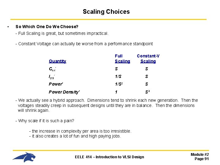
Scaling Choices • So Which One Do We Choose? - Full Scaling is great, but sometimes impractical. - Constant Voltage can actually be worse from a performance standpoint Quantity Full Scaling Constant-V Scaling Cox' S S IDS' 1/S S Power' 1/S 2 S Power Density' 1 S 3 - We actually see a hybrid approach. Dimensions tend to shrink each new generation. Then the voltages steadily creep in subsequent designs until they are in balance. Then the dimensions will shrink again. - Why scale if it is such a pain? - the increase in complexity per area is too irresistible. - it also creates a lot of fun and high paying jobs. EELE 414 – Introduction to VLSI Design Module #2 Page 91

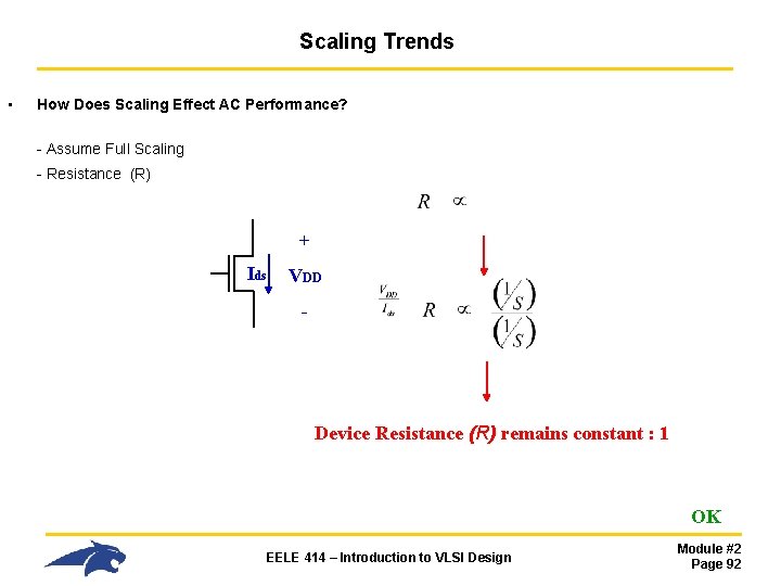
Scaling Trends • How Does Scaling Effect AC Performance? - Assume Full Scaling - Resistance (R) + Ids VDD - Device Resistance (R) remains constant : 1 OK EELE 414 – Introduction to VLSI Design Module #2 Page 92

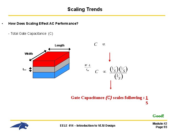
Scaling Trends • How Does Scaling Effect AC Performance? - Total Gate Capacitance (C) Length Width tox Gate Capacitance (C) scales following : 1 S Good! EELE 414 – Introduction to VLSI Design Module #2 Page 93

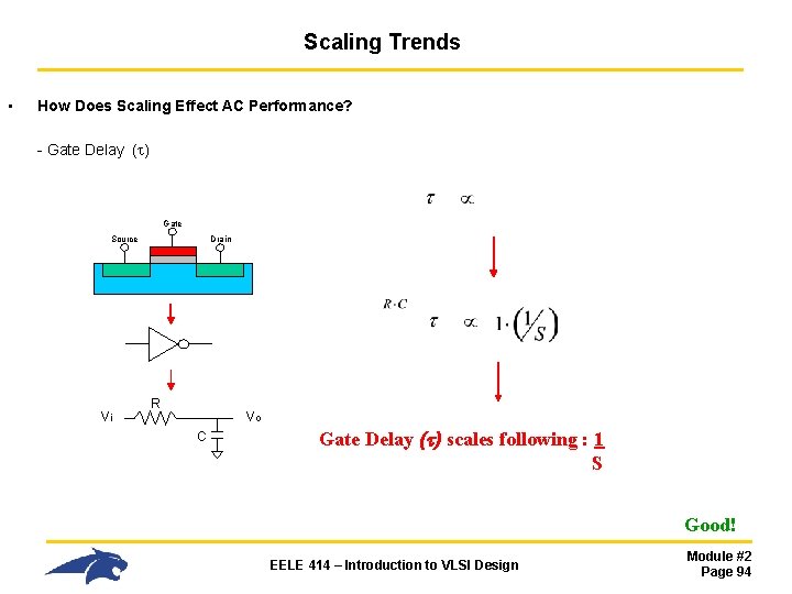
Scaling Trends • How Does Scaling Effect AC Performance? - Gate Delay ( ) Gate Source Vi Drain R Vo C Gate Delay ( ) scales following : 1 S Good! EELE 414 – Introduction to VLSI Design Module #2 Page 94

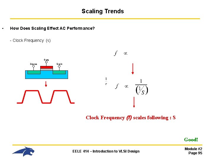
Scaling Trends • How Does Scaling Effect AC Performance? - Clock Frequency ( ) Gate Source Drain Clock Frequency (f) scales following : S Good! EELE 414 – Introduction to VLSI Design Module #2 Page 95

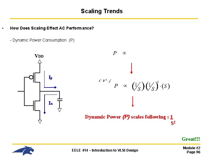
Scaling Trends • How Does Scaling Effect AC Performance? - Dynamic Power Consumption (P) VDD Ip In Dynamic Power (P) scales following : 1 S 2 Great!!! EELE 414 – Introduction to VLSI Design Module #2 Page 96

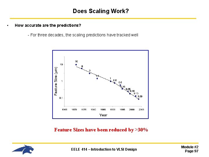
Does Scaling Work? • How accurate are the predictions? - For three decades, the scaling predictions have tracked well Feature Sizes have been reduced by >30% EELE 414 – Introduction to VLSI Design Module #2 Page 97

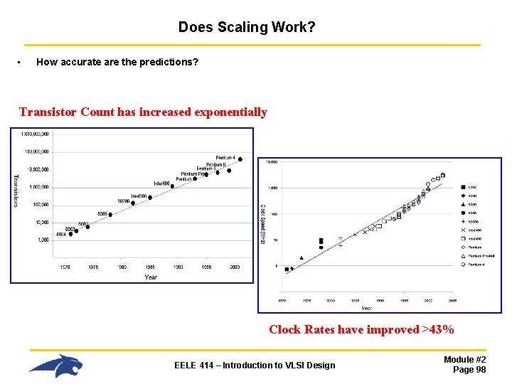
Does Scaling Work? • How accurate are the predictions? Transistor Count has increased exponentially Clock Rates have improved >43% EELE 414 – Introduction to VLSI Design Module #2 Page 98

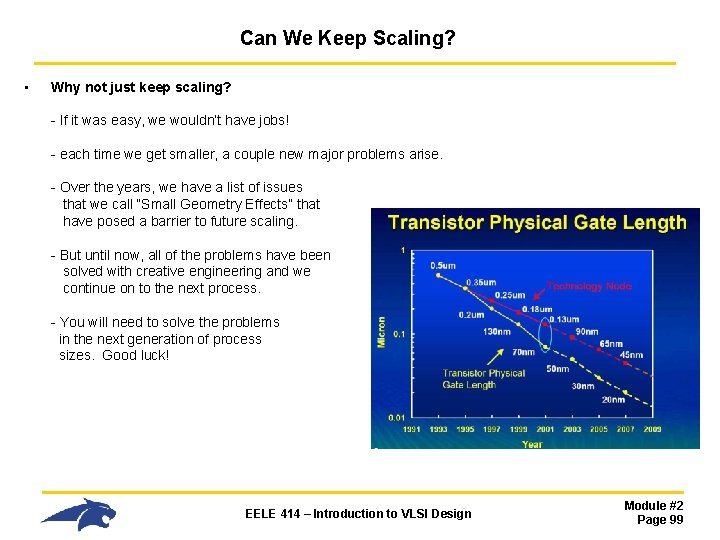
Can We Keep Scaling? • Why not just keep scaling? - If it was easy, we wouldn’t have jobs! - each time we get smaller, a couple new major problems arise. - Over the years, we have a list of issues that we call “Small Geometry Effects” that have posed a barrier to future scaling. - But until now, all of the problems have been solved with creative engineering and we continue on to the next process. - You will need to solve the problems in the next generation of process sizes. Good luck! EELE 414 – Introduction to VLSI Design Module #2 Page 99

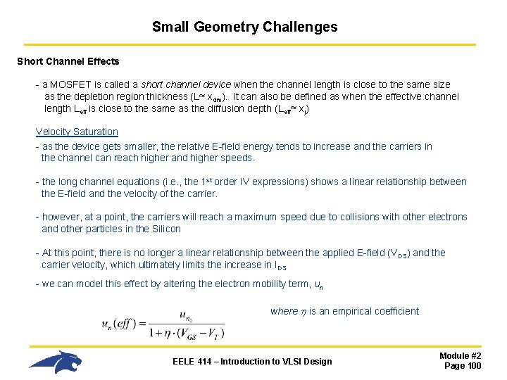
Small Geometry Challenges Short Channel Effects - a MOSFET is called a short channel device when the channel length is close to the same size as the depletion region thickness (L≈ xdm). It can also be defined as when the effective channel length Leff is close to the same as the diffusion depth (Leff≈ xj) Velocity Saturation - as the device gets smaller, the relative E-field energy tends to increase and the carriers in the channel can reach higher and higher speeds. - the long channel equations (i. e. , the 1 st order IV expressions) shows a linear relationship between the E-field and the velocity of the carrier. - however, at a point, the carriers will reach a maximum speed due to collisions with other electrons and other particles in the Silicon - At this point, there is no longer a linear relationship between the applied E-field (V DS) and the carrier velocity, which ultimately limits the increase in IDS - we can model this effect by altering the electron mobility term, un where is an empirical coefficient EELE 414 – Introduction to VLSI Design Module #2 Page 100

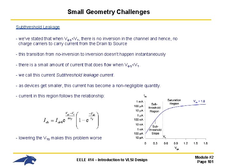
Small Geometry Challenges Subthreshold Leakage - we’ve stated that when VGS<VT, there is no inversion in the channel and hence, no charge carriers to carry current from the Drain to Source - this transition from no-inversion to inversion doesn’t happen instantaneously - there is a small amount of current that does flow when VGS<VT. - we call this current Subthreshold leakage current. - as devices get smaller, this current has become a non-negligible quantity. - current in this region follows the relationship: - lowering the VT 0 makes this problem worse EELE 414 – Introduction to VLSI Design Module #2 Page 101

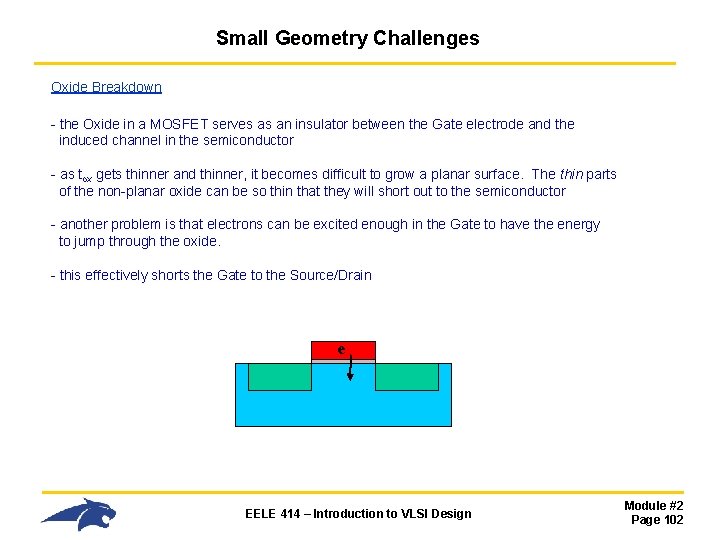
Small Geometry Challenges Oxide Breakdown - the Oxide in a MOSFET serves as an insulator between the Gate electrode and the induced channel in the semiconductor - as tox gets thinner and thinner, it becomes difficult to grow a planar surface. The thin parts of the non-planar oxide can be so thin that they will short out to the semiconductor - another problem is that electrons can be excited enough in the Gate to have the energy to jump through the oxide. - this effectively shorts the Gate to the Source/Drain e EELE 414 – Introduction to VLSI Design Module #2 Page 102

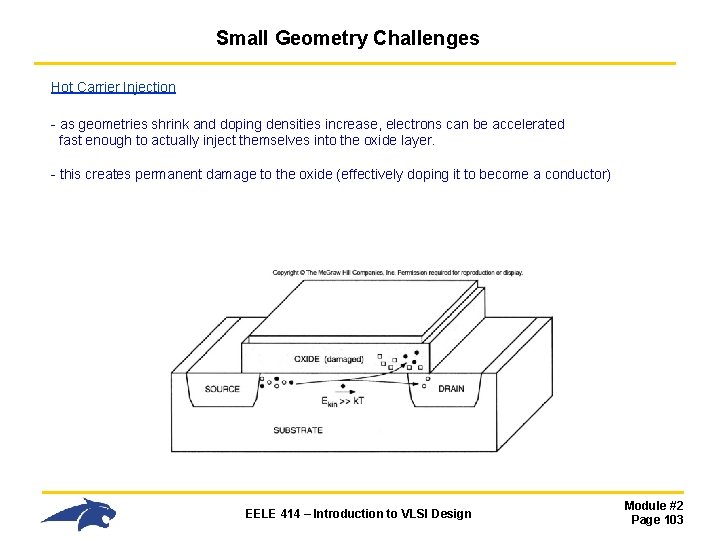
Small Geometry Challenges Hot Carrier Injection - as geometries shrink and doping densities increase, electrons can be accelerated fast enough to actually inject themselves into the oxide layer. - this creates permanent damage to the oxide (effectively doping it to become a conductor) EELE 414 – Introduction to VLSI Design Module #2 Page 103

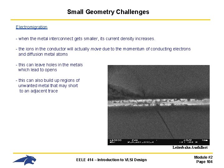
Small Geometry Challenges Electromigration - when the metal interconnect gets smaller, its current density increases. - the ions in the conductor will actually move due to the momentum of conducting electrons and diffusion metal atoms - this can leave holes in the metals which lead to opens - this can also build up regions of unwanted metal that may short to an adjacent trace Leiterbahn Ausfallort EELE 414 – Introduction to VLSI Design Module #2 Page 104

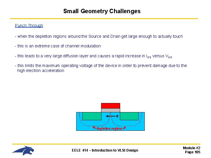
Small Geometry Challenges Punch Through - when the depletion regions around the Source and Drain get large enough to actually touch - this is an extreme case of channel modulation - this leads to a very large diffusion layer and causes a rapid increase in IDS versus VDS - this limits the maximum operating voltage of the device in order to prevent damage due to the high electron acceleration e depletion regions EELE 414 – Introduction to VLSI Design Module #2 Page 105

Small Geometry Challenges Drain Induced Barrier Lowering (DIBL) - if the gate length is scaled without properly scaling the Source/Drain regions, the Drain voltage will cause an un-proportionally large inversion layer - this inversion interferes with the desired inversion layer being created by the Gate voltage - this effectively lowers the Threshold voltage because it takes less energy to create inversion since the Drain is providing some inversion itself. EELE 414 – Introduction to VLSI Design Module #2 Page 106

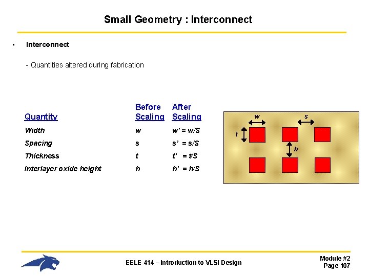
Small Geometry : Interconnect • Interconnect - Quantities altered during fabrication Quantity Before After Scaling Width w w’ = w/S Spacing s s’ = s/S Thickness t t’ = t/S Interlayer oxide height h h’ = h/S w s t EELE 414 – Introduction to VLSI Design h Module #2 Page 107

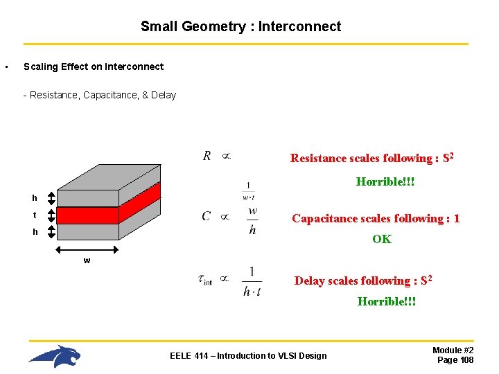
Small Geometry : Interconnect • Scaling Effect on Interconnect - Resistance, Capacitance, & Delay Resistance scales following : S 2 Horrible!!! h t Capacitance scales following : 1 h OK w Delay scales following : S 2 Horrible!!! EELE 414 – Introduction to VLSI Design Module #2 Page 108

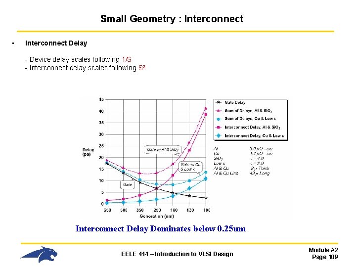
Small Geometry : Interconnect • Interconnect Delay - Device delay scales following 1/S - Interconnect delay scales following S 2 Interconnect Delay Dominates below 0. 25 um EELE 414 – Introduction to VLSI Design Module #2 Page 109

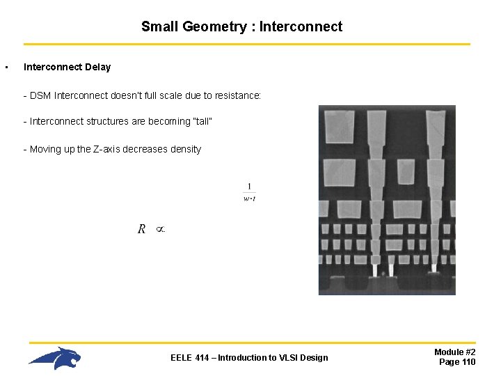
Small Geometry : Interconnect • Interconnect Delay - DSM Interconnect doesn’t full scale due to resistance: - Interconnect structures are becoming “tall” - Moving up the Z-axis decreases density EELE 414 – Introduction to VLSI Design Module #2 Page 110

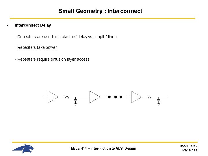
Small Geometry : Interconnect • Interconnect Delay - Repeaters are used to make the “delay vs. length” linear - Repeaters take power - Repeaters require diffusion layer access EELE 414 – Introduction to VLSI Design Module #2 Page 111

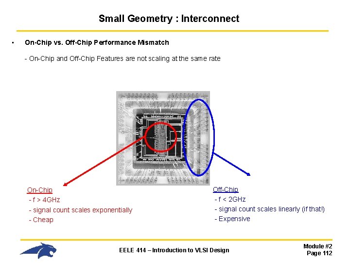
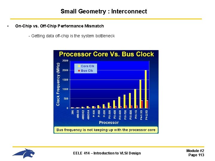
Small Geometry : Interconnect • On-Chip vs. Off-Chip Performance Mismatch - On-Chip and Off-Chip Features are not scaling at the same rate On-Chip - f > 4 GHz - signal count scales exponentially - Cheap Off-Chip - f < 2 GHz - signal count scales linearly (if that!) - Expensive EELE 414 – Introduction to VLSI Design Module #2 Page 112

Small Geometry : Interconnect • On-Chip vs. Off-Chip Performance Mismatch - Getting data off-chip is the system bottleneck EELE 414 – Introduction to VLSI Design Module #2 Page 113

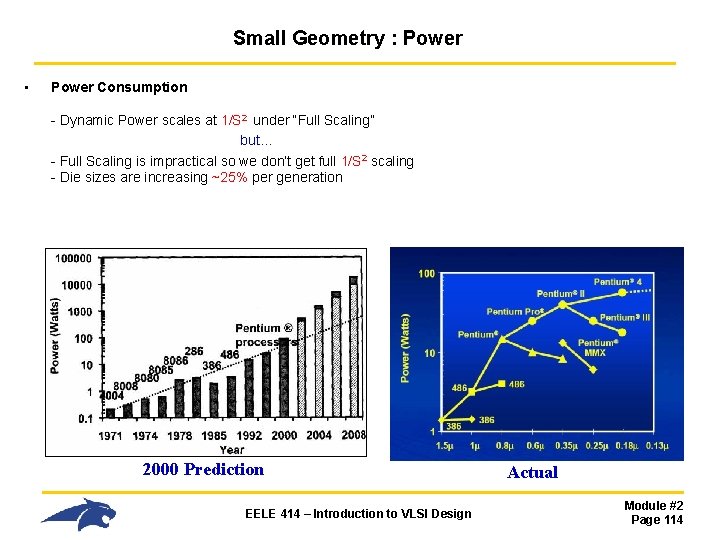
Small Geometry : Power • Power Consumption - Dynamic Power scales at 1/S 2 under “Full Scaling” but… - Full Scaling is impractical so we don’t get full 1/S 2 scaling - Die sizes are increasing ~25% per generation 2000 Prediction EELE 414 – Introduction to VLSI Design Actual Module #2 Page 114

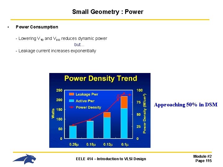
Small Geometry : Power • Power Consumption - Lowering VT 0 and VDD reduces dynamic power but… - Leakage current increases exponentially Approaching 50% in DSM EELE 414 – Introduction to VLSI Design Module #2 Page 115

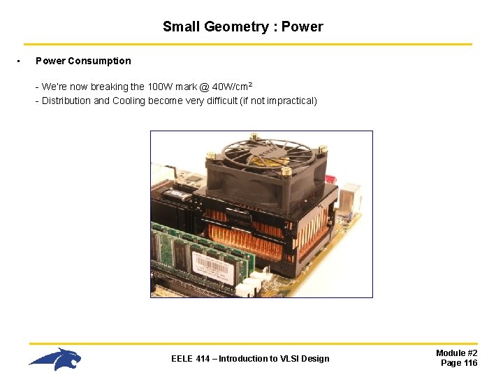
Small Geometry : Power • Power Consumption - We’re now breaking the 100 W mark @ 40 W/cm 2 - Distribution and Cooling become very difficult (if not impractical) EELE 414 – Introduction to VLSI Design Module #2 Page 116

MOSFET Capacitance • MOSFET Capacitance - We have looked at device physics of the MOS structure - We have also looked at the DC I-V characteristics of the MOS Transistors - We have not looked at AC performance - Capacitance is the dominating imaginary component on-chip (i. e. , we don't really have inductance) - the Capacitances of a MOSFET are considered parasitic - "parasitic" means unwanted or unintentional. They are unavoidable and a result of fabricating the devices using physical materials. - we can use the capacitances of the MOSFET to estimate factors such as rise time, delay, fan-out, and propagation delay EELE 414 – Introduction to VLSI Design Module #2 Page 117

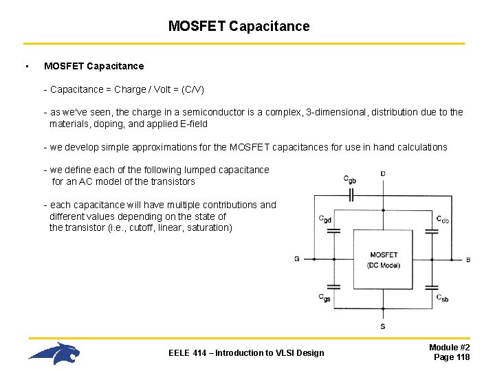
MOSFET Capacitance • MOSFET Capacitance - Capacitance = Charge / Volt = (C/V) - as we've seen, the charge in a semiconductor is a complex, 3 -dimensional, distribution due to the materials, doping, and applied E-field - we develop simple approximations for the MOSFET capacitances for use in hand calculations - we define each of the following lumped capacitance for an AC model of the transistors - each capacitance will have multiple contributions and different values depending on the state of the transistor (i. e. , cutoff, linear, saturation) EELE 414 – Introduction to VLSI Design Module #2 Page 118

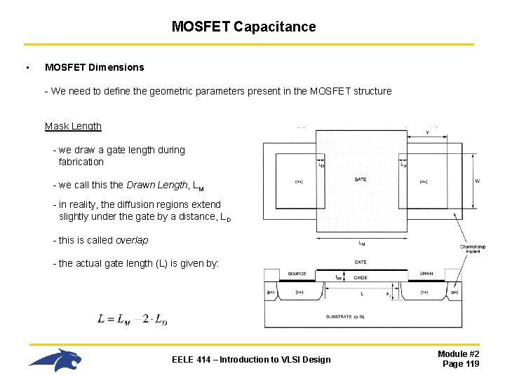
MOSFET Capacitance • MOSFET Dimensions - We need to define the geometric parameters present in the MOSFET structure Mask Length - we draw a gate length during fabrication - we call this the Drawn Length, LM - in reality, the diffusion regions extend slightly under the gate by a distance, LD - this is called overlap - the actual gate length (L) is given by: EELE 414 – Introduction to VLSI Design Module #2 Page 119

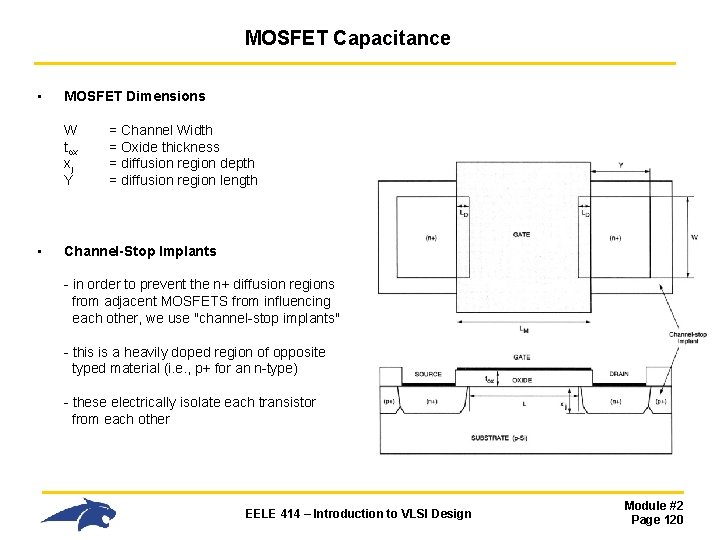
MOSFET Capacitance • MOSFET Dimensions W tox xj Y • = Channel Width = Oxide thickness = diffusion region depth = diffusion region length Channel-Stop Implants - in order to prevent the n+ diffusion regions from adjacent MOSFETS from influencing each other, we use "channel-stop implants" - this is a heavily doped region of opposite typed material (i. e. , p+ for an n-type) - these electrically isolate each transistor from each other EELE 414 – Introduction to VLSI Design Module #2 Page 120

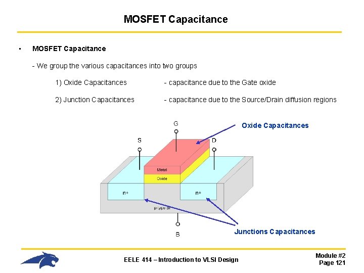
MOSFET Capacitance • MOSFET Capacitance - We group the various capacitances into two groups 1) Oxide Capacitances - capacitance due to the Gate oxide 2) Junction Capacitances - capacitance due to the Source/Drain diffusion regions Oxide Capacitances Junctions Capacitances EELE 414 – Introduction to VLSI Design Module #2 Page 121

Oxide-Related Capacitance • Oxide-Capacitance - Oxide Capacitance refers to capacitance which uses the gate oxide as the insulator between the parallel plates of the capacitor - as a result, these capacitances always use the Gate as one of the terminals of the capacitor - we are concerned with the following capacitances: Cgb Cgd Cgs = Gate to Body capacitance = Gate to Drain capacitance = Gate to Source capacitance - again, each of these values will differ depending on the mode of operation of the MOSFET EELE 414 – Introduction to VLSI Design Module #2 Page 122

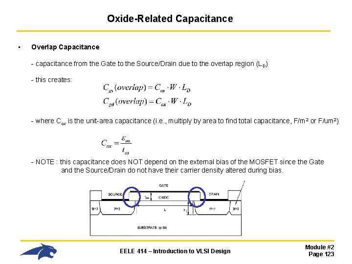
Oxide-Related Capacitance • Overlap Capacitance - capacitance from the Gate to the Source/Drain due to the overlap region (LD) - this creates: - where Cox is the unit-area capacitance (i. e. , multiply by area to find total capacitance, F/m 2 or F/um 2) - NOTE : this capacitance does NOT depend on the external bias of the MOSFET since the Gate and the Source/Drain do not have their carrier density altered during bias. EELE 414 – Introduction to VLSI Design Module #2 Page 123

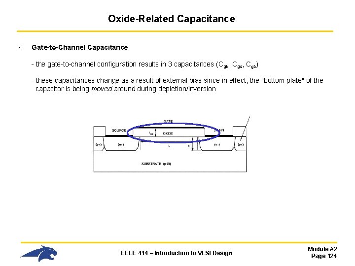
Oxide-Related Capacitance • Gate-to-Channel Capacitance - the gate-to-channel configuration results in 3 capacitances (Cgb, Cgs, Cgb) - these capacitances change as a result of external bias since in effect, the "bottom plate" of the capacitor is being moved around during depletion/inversion EELE 414 – Introduction to VLSI Design Module #2 Page 124

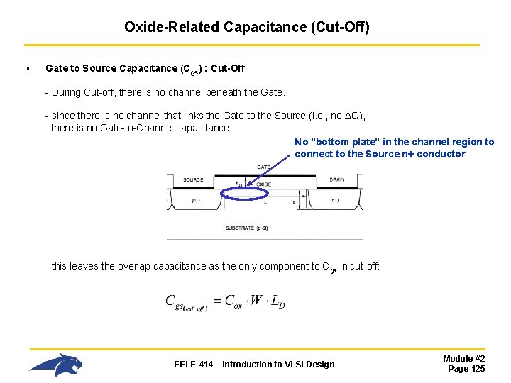
Oxide-Related Capacitance (Cut-Off) • Gate to Source Capacitance (Cgs) : Cut-Off - During Cut-off, there is no channel beneath the Gate. - since there is no channel that links the Gate to the Source (i. e. , no ΔQ), there is no Gate-to-Channel capacitance. No "bottom plate" in the channel region to connect to the Source n+ conductor - this leaves the overlap capacitance as the only component to Cgs in cut-off: EELE 414 – Introduction to VLSI Design Module #2 Page 125

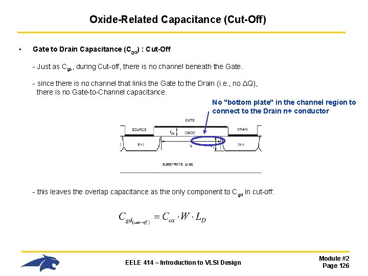
Oxide-Related Capacitance (Cut-Off) • Gate to Drain Capacitance (Cgd) : Cut-Off - Just as Cgs, during Cut-off, there is no channel beneath the Gate. - since there is no channel that links the Gate to the Drain (i. e. , no ΔQ), there is no Gate-to-Channel capacitance. No "bottom plate" in the channel region to connect to the Drain n+ conductor - this leaves the overlap capacitance as the only component to Cgd in cut-off: EELE 414 – Introduction to VLSI Design Module #2 Page 126

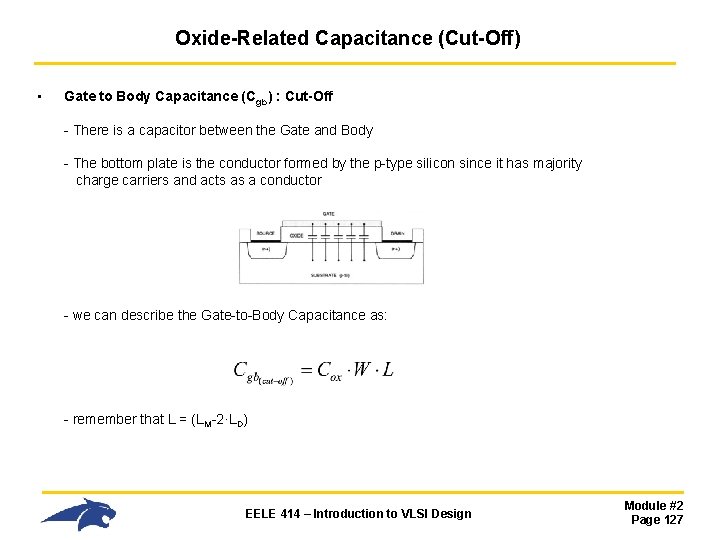
Oxide-Related Capacitance (Cut-Off) • Gate to Body Capacitance (Cgb) : Cut-Off - There is a capacitor between the Gate and Body - The bottom plate is the conductor formed by the p-type silicon since it has majority charge carriers and acts as a conductor - we can describe the Gate-to-Body Capacitance as: - remember that L = (LM-2·LD) EELE 414 – Introduction to VLSI Design Module #2 Page 127

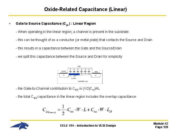
Oxide-Related Capacitance (Linear) • Gate to Source Capacitance (Cgs) : Linear Region - When operating in the linear region, a channel is present in the substrate. - this can be thought of as a conductor (or metal plate) that contacts the Source and Drain - this results in a capacitance between the Gate and the Source/Drain - we split this capacitance between the Source and Drain for simplicity - the Gate-to-Channel contribution to CGS is (1/2)Cox. WL - the total CGS capacitance in the linear region includes the overlap capacitance: EELE 414 – Introduction to VLSI Design Module #2 Page 128

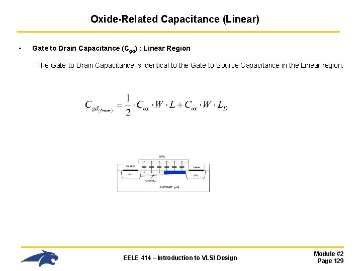
Oxide-Related Capacitance (Linear) • Gate to Drain Capacitance (Cgd) : Linear Region - The Gate-to-Drain Capacitance is identical to the Gate-to-Source Capacitance in the Linear region: EELE 414 – Introduction to VLSI Design Module #2 Page 129

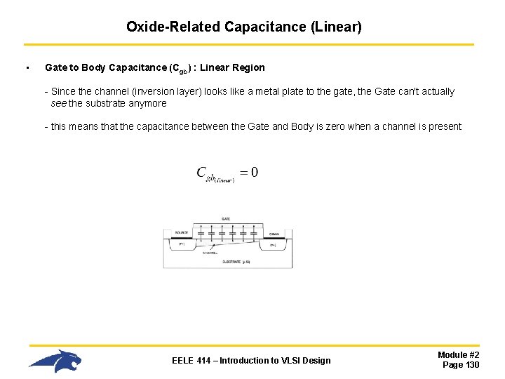
Oxide-Related Capacitance (Linear) • Gate to Body Capacitance (Cgb) : Linear Region - Since the channel (inversion layer) looks like a metal plate to the gate, the Gate can't actually see the substrate anymore - this means that the capacitance between the Gate and Body is zero when a channel is present EELE 414 – Introduction to VLSI Design Module #2 Page 130

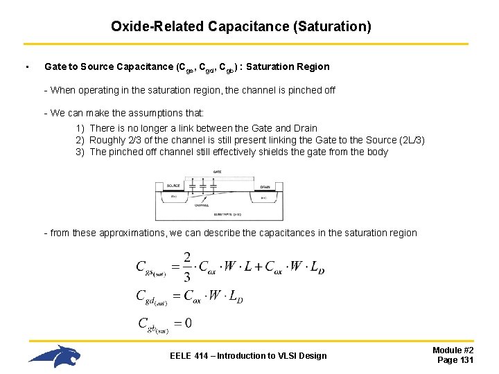
Oxide-Related Capacitance (Saturation) • Gate to Source Capacitance (Cgs, Cgd, Cgb) : Saturation Region - When operating in the saturation region, the channel is pinched off - We can make the assumptions that: 1) There is no longer a link between the Gate and Drain 2) Roughly 2/3 of the channel is still present linking the Gate to the Source (2 L/3) 3) The pinched off channel still effectively shields the gate from the body - from these approximations, we can describe the capacitances in the saturation region EELE 414 – Introduction to VLSI Design Module #2 Page 131

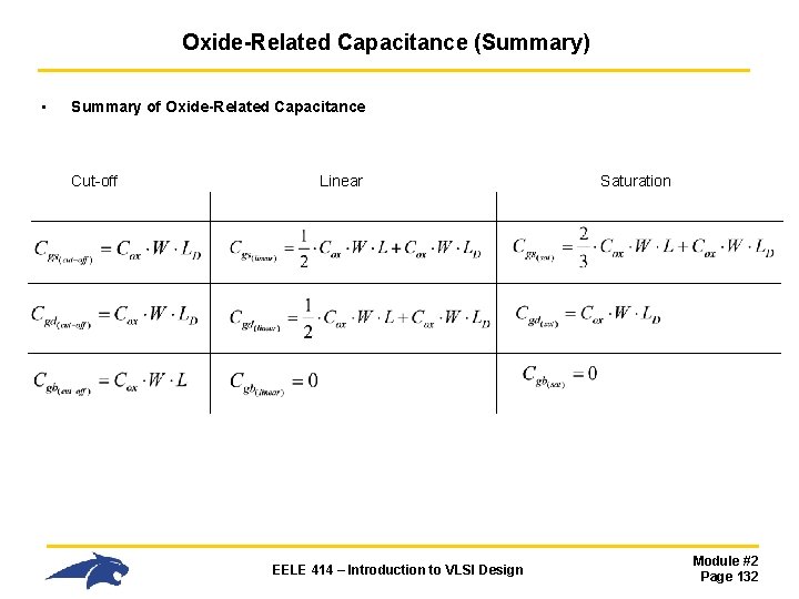
Oxide-Related Capacitance (Summary) • Summary of Oxide-Related Capacitance Cut-off Linear EELE 414 – Introduction to VLSI Design Saturation Module #2 Page 132

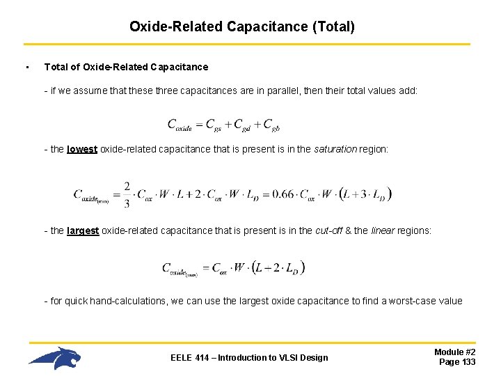
Oxide-Related Capacitance (Total) • Total of Oxide-Related Capacitance - if we assume that these three capacitances are in parallel, then their total values add: - the lowest oxide-related capacitance that is present is in the saturation region: - the largest oxide-related capacitance that is present is in the cut-off & the linear regions: - for quick hand-calculations, we can use the largest oxide capacitance to find a worst-case value EELE 414 – Introduction to VLSI Design Module #2 Page 133

Junction Capacitance • Junction Capacitance - Junction Capacitance refers to capacitance between the diffusion regions of the Source & Drain to the doped substrate surrounding them. - they are called "junction" because these capacitances are due to the PN junctions that are formed between the two materials - we are concerned with the following junction capacitances: Csb Cdb = Source to Body capacitance = Drain to Body capacitance - these capacitances are highly dependant on the bias voltages since the effective distance between plates is the depth of the built in depletion region that forms at the PN junction EELE 414 – Introduction to VLSI Design Module #2 Page 134

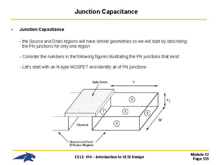
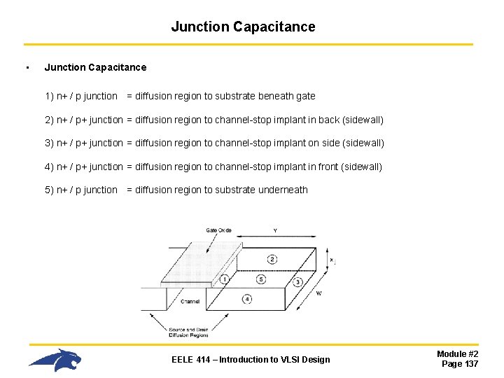
Junction Capacitance • Junction Capacitance - the Source and Drain regions will have similar geometries so we will start by describing the PN junctions for only one region - Consider the numbers in the following figures illustrating the PN junctions that exist - Let's start with an N-type MOSFET and identify all of PN junctions EELE 414 – Introduction to VLSI Design Module #2 Page 135

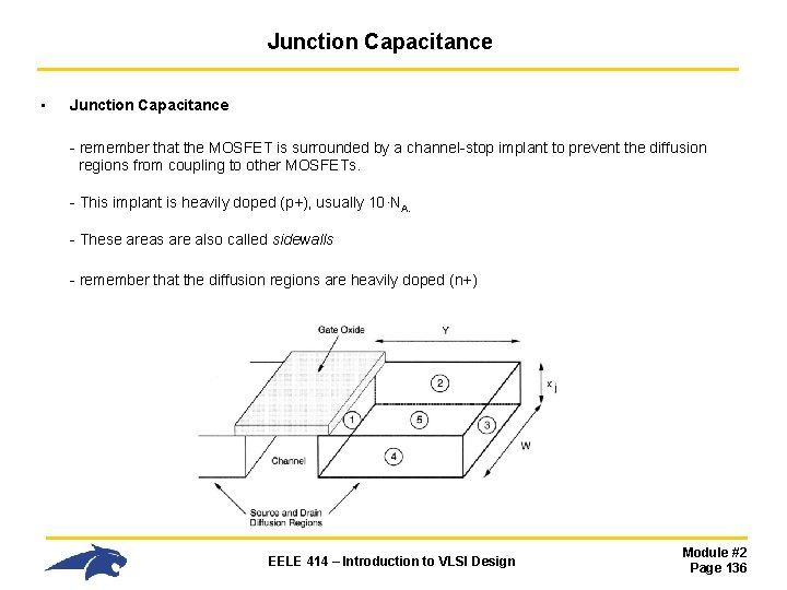
Junction Capacitance • Junction Capacitance - remember that the MOSFET is surrounded by a channel-stop implant to prevent the diffusion regions from coupling to other MOSFETs. - This implant is heavily doped (p+), usually 10·NA. - These areas are also called sidewalls - remember that the diffusion regions are heavily doped (n+) EELE 414 – Introduction to VLSI Design Module #2 Page 136

Junction Capacitance • Junction Capacitance 1) n+ / p junction = diffusion region to substrate beneath gate 2) n+ / p+ junction = diffusion region to channel-stop implant in back (sidewall) 3) n+ / p+ junction = diffusion region to channel-stop implant on side (sidewall) 4) n+ / p+ junction = diffusion region to channel-stop implant in front (sidewall) 5) n+ / p junction = diffusion region to substrate underneath EELE 414 – Introduction to VLSI Design Module #2 Page 137

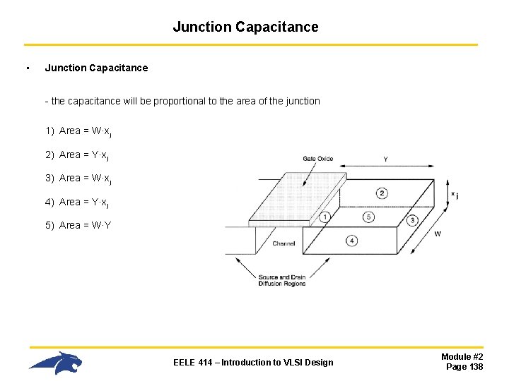
Junction Capacitance • Junction Capacitance - the capacitance will be proportional to the area of the junction 1) Area = W·xj 2) Area = Y·xj 3) Area = W·xj 4) Area = Y·xj 5) Area = W·Y EELE 414 – Introduction to VLSI Design Module #2 Page 138

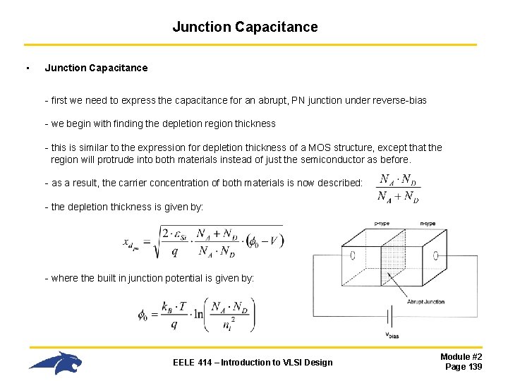
Junction Capacitance • Junction Capacitance - first we need to express the capacitance for an abrupt, PN junction under reverse-bias - we begin with finding the depletion region thickness - this is similar to the expression for depletion thickness of a MOS structure, except that the region will protrude into both materials instead of just the semiconductor as before. - as a result, the carrier concentration of both materials is now described: - the depletion thickness is given by: - where the built in junction potential is given by: EELE 414 – Introduction to VLSI Design Module #2 Page 139

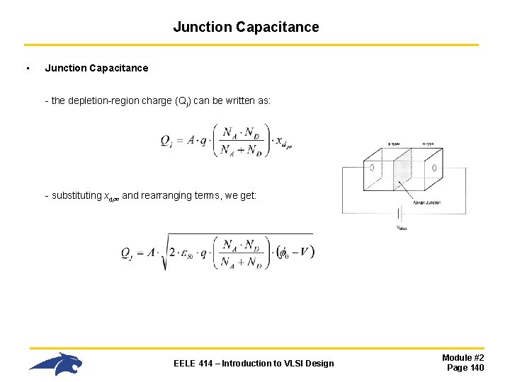
Junction Capacitance • Junction Capacitance - the depletion-region charge (Qj) can be written as: - substituting xdpn and rearranging terms, we get: EELE 414 – Introduction to VLSI Design Module #2 Page 140

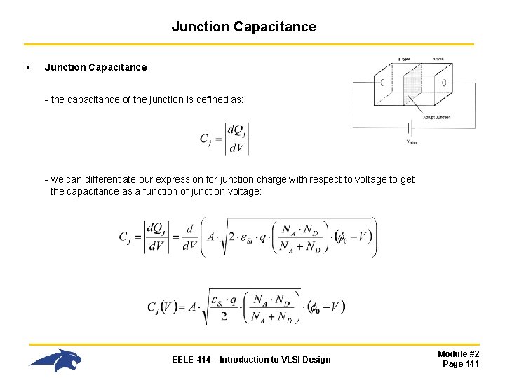
Junction Capacitance • Junction Capacitance - the capacitance of the junction is defined as: - we can differentiate our expression for junction charge with respect to voltage to get the capacitance as a function of junction voltage: EELE 414 – Introduction to VLSI Design Module #2 Page 141

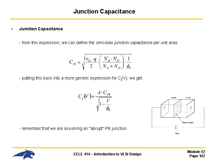
Junction Capacitance • Junction Capacitance - from this expression, we can define the zero-bias junction capacitance per unit area: - putting this back into a more generic expression for Cj(V), we get: - remember that we are assuming an "abrupt" PN junction EELE 414 – Introduction to VLSI Design Module #2 Page 142

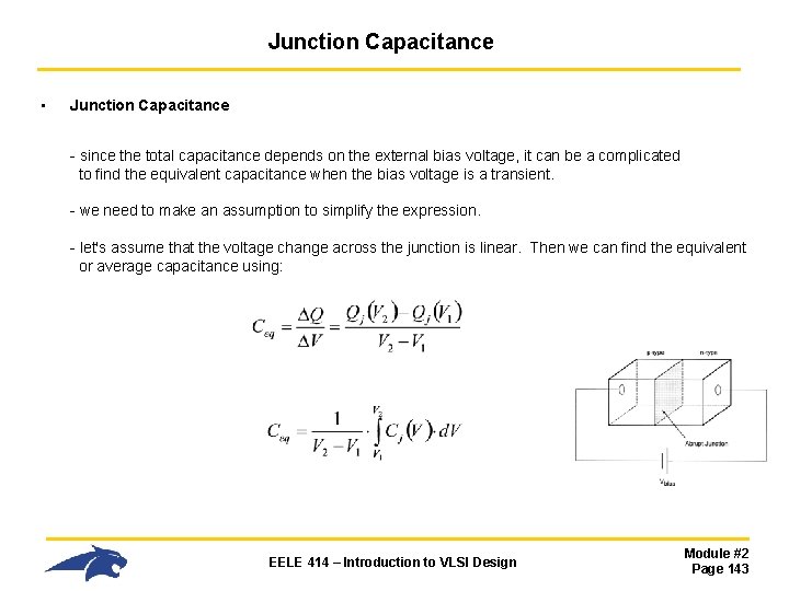
Junction Capacitance • Junction Capacitance - since the total capacitance depends on the external bias voltage, it can be a complicated to find the equivalent capacitance when the bias voltage is a transient. - we need to make an assumption to simplify the expression. - let's assume that the voltage change across the junction is linear. Then we can find the equivalent or average capacitance using: EELE 414 – Introduction to VLSI Design Module #2 Page 143

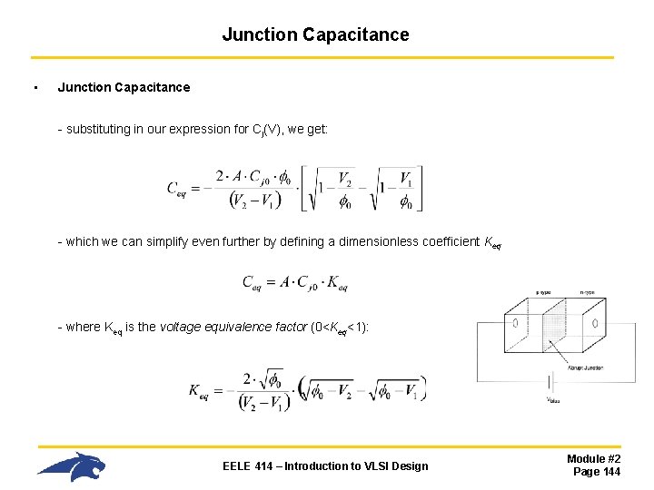
Junction Capacitance • Junction Capacitance - substituting in our expression for Cj(V), we get: - which we can simplify even further by defining a dimensionless coefficient Keq - where Keq is the voltage equivalence factor (0<Keq<1): EELE 414 – Introduction to VLSI Design Module #2 Page 144

Junction Capacitance • Junction Capacitance - How do we use this? - for a given diffusion region, we calculate Ceq for each of the 5 PN junctions - note that there really are only two different regions (n+ / p and n+ / p+) - the sidewalls (2, 3, 4) will have their own zero-bias junction capacitance since they have a unique carrier concentration (i. e. , n+ / p+). - the inner and bottom junctions (1, 5) will have their own zero-bias junction capacitance since they have a unique carrier concentration (i. e. , n+ / p). - when solving for the sidewall contribution, you can add the areas for 2, 3, 4 and solve once - when solving for the inner and bottom junction contributions, you can add the areas for 1 and 5 and solve once - since this is a reverse biased PN junction the voltages for V 1 and V 2 are actually negative when plugged into the Keq expression EELE 414 – Introduction to VLSI Design Module #2 Page 145

Junction Capacitance • Junction Capacitance - What's the difference between the Source and Drain? - If the Source is grounded, then there is no voltage change across it. This means its capacitance is simply the zero-bias capacitance - you will still need to calculate the sidewall and inner/bottom Cj 0 capacitances separately - the drain typically sees a voltage change (VDS). However, one good thing is that typically the source voltage is 0 v, so the expression simplifies somewhat EELE 414 – Introduction to VLSI Design Module #2 Page 146

Junction Capacitance • Junction Capacitance - Doesn't this take a lot of time? - Yes! And remember that we have made a lot of assumptions along the way - For this reason, we typically rely on computer models of the capacitance - We do the hand calculations to get a gut feel for what factors affect capacitance - Gut Feel makes for good designers because design is about balancing trade-offs - If you don’t have Gut Feel and rely totally on simulators, you will struggle when asked to innovate and trouble-shoot. EELE 414 – Introduction to VLSI Design Module #2 Page 147