VLSI Design DC Transient Response EE 447 VLSI
- Slides: 47

VLSI Design DC & Transient Response EE 447 VLSI Design 4: DC and Transient Response 1

Outline n n DC Response Logic Levels and Noise Margins Transient Response Delay Estimation EE 447 VLSI Design 4: DC and Transient Response 2

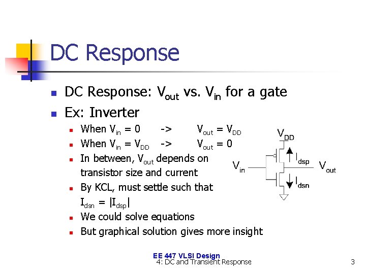
DC Response n n DC Response: Vout vs. Vin for a gate Ex: Inverter n n n When Vin = 0 -> Vout = VDD When Vin = VDD -> Vout = 0 In between, Vout depends on transistor size and current By KCL, must settle such that Idsn = |Idsp| We could solve equations But graphical solution gives more insight EE 447 VLSI Design 4: DC and Transient Response 3

Transistor Operation n n Current depends on region of transistor behavior For what Vin and Vout are n. MOS and p. MOS in n Cutoff? Linear? Saturation? EE 447 VLSI Design 4: DC and Transient Response 4

I-V Characteristics n Make p. MOS is wider than n. MOS such that bn = bp EE 447 VLSI Design 4: DC and Transient Response 5

Current vs. Vout, Vin EE 447 VLSI Design 4: DC and Transient Response 6

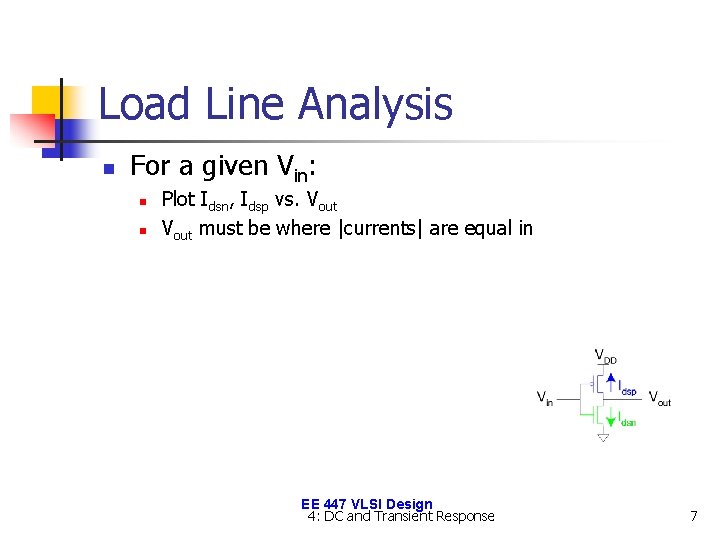
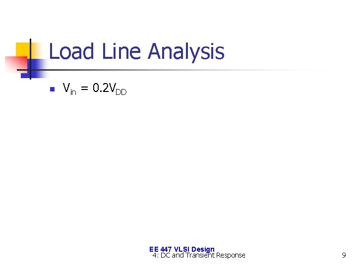
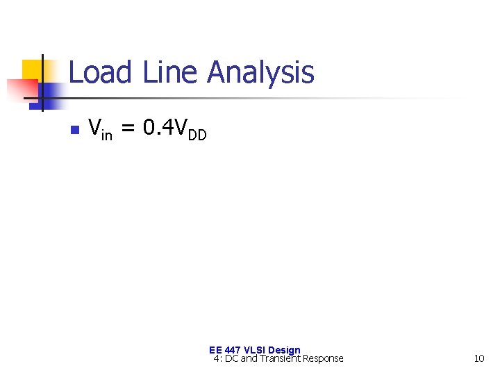
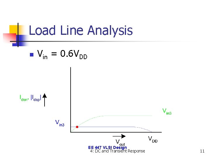
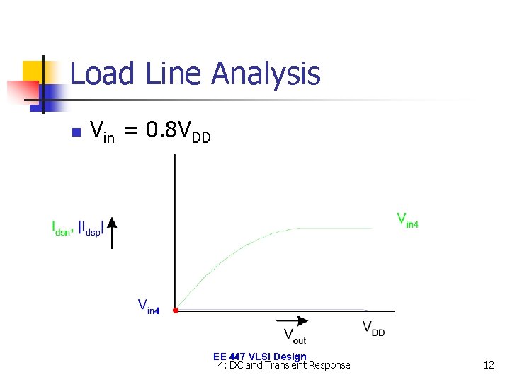
Load Line Analysis n For a given Vin: n n Plot Idsn, Idsp vs. Vout must be where |currents| are equal in EE 447 VLSI Design 4: DC and Transient Response 7

Load Line Analysis n Vin = 0 EE 447 VLSI Design 4: DC and Transient Response 8

Load Line Analysis n Vin = 0. 2 VDD EE 447 VLSI Design 4: DC and Transient Response 9

Load Line Analysis n Vin = 0. 4 VDD EE 447 VLSI Design 4: DC and Transient Response 10

Load Line Analysis n Vin = 0. 6 VDD EE 447 VLSI Design 4: DC and Transient Response 11

Load Line Analysis n Vin = 0. 8 VDD EE 447 VLSI Design 4: DC and Transient Response 12

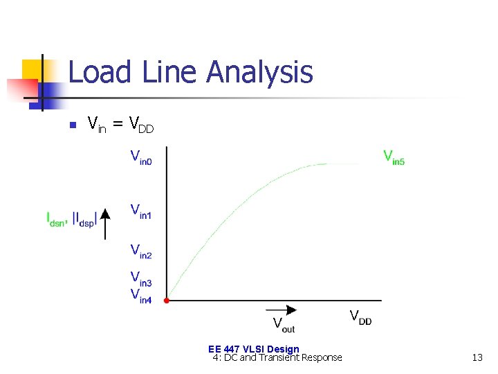
Load Line Analysis n Vin = VDD EE 447 VLSI Design 4: DC and Transient Response 13

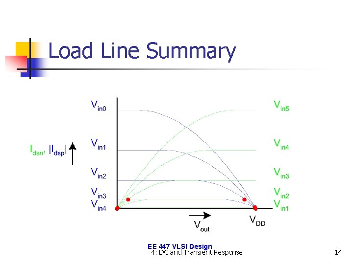
Load Line Summary EE 447 VLSI Design 4: DC and Transient Response 14

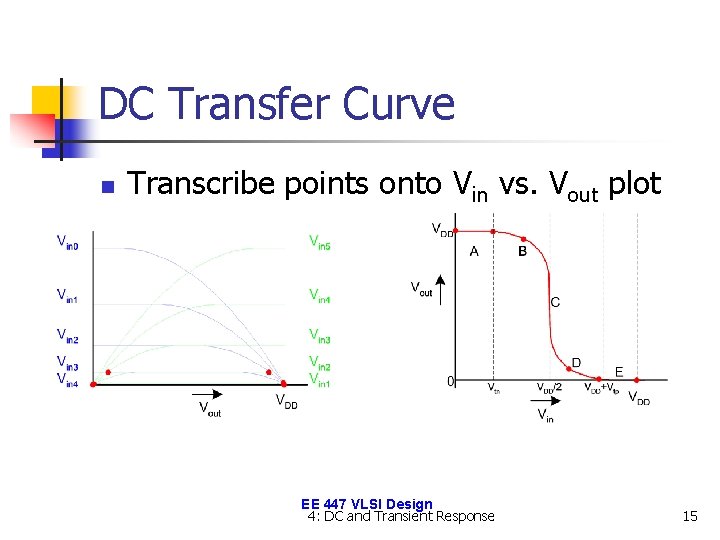
DC Transfer Curve n Transcribe points onto Vin vs. Vout plot EE 447 VLSI Design 4: DC and Transient Response 15

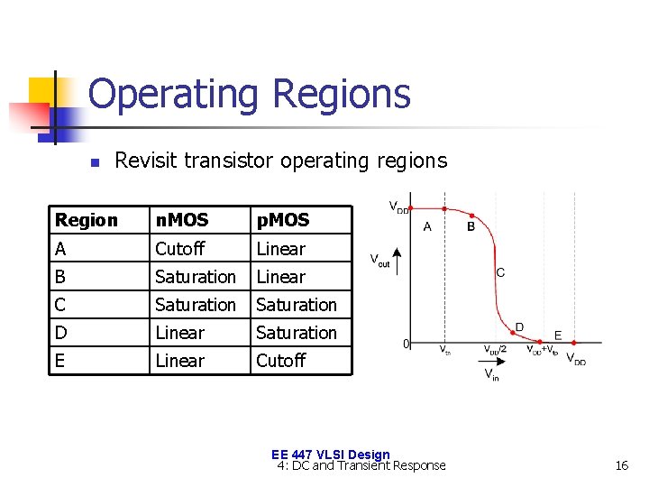
Operating Regions n Revisit transistor operating regions Region n. MOS p. MOS A Cutoff Linear B Saturation Linear C Saturation D Linear Saturation E Linear Cutoff EE 447 VLSI Design 4: DC and Transient Response 16

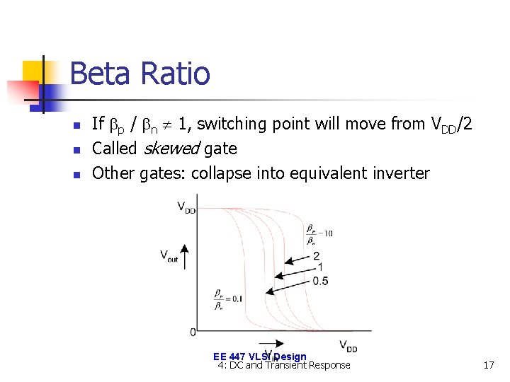
Beta Ratio n n n If bp / bn 1, switching point will move from VDD/2 Called skewed gate Other gates: collapse into equivalent inverter EE 447 VLSI Design 4: DC and Transient Response 17

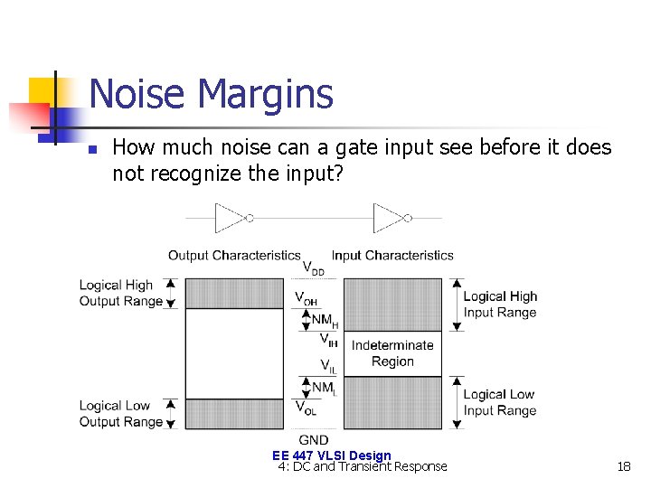
Noise Margins n How much noise can a gate input see before it does not recognize the input? EE 447 VLSI Design 4: DC and Transient Response 18

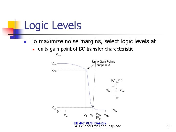
Logic Levels n To maximize noise margins, select logic levels at n unity gain point of DC transfer characteristic EE 447 VLSI Design 4: DC and Transient Response 19

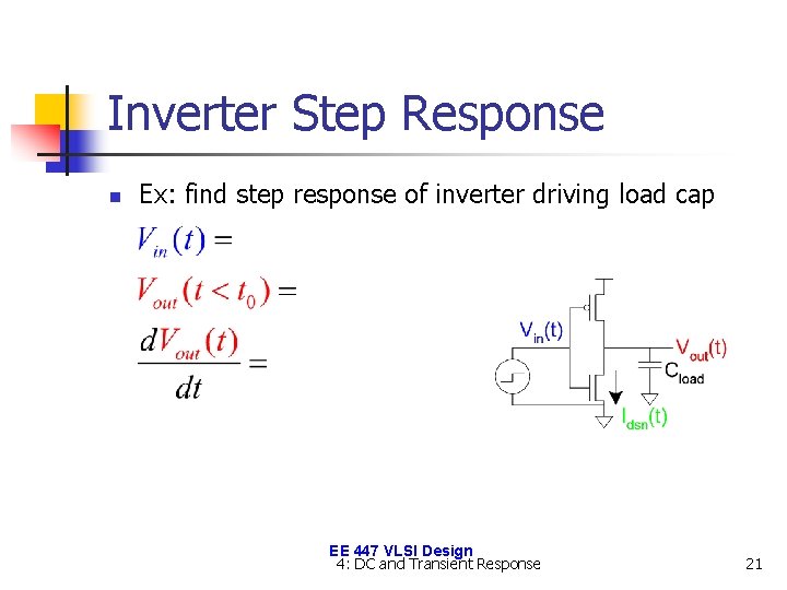
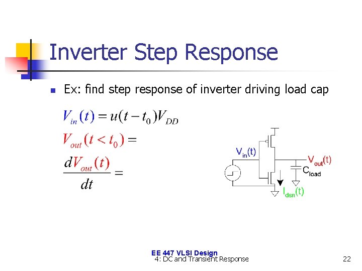
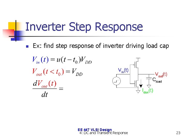
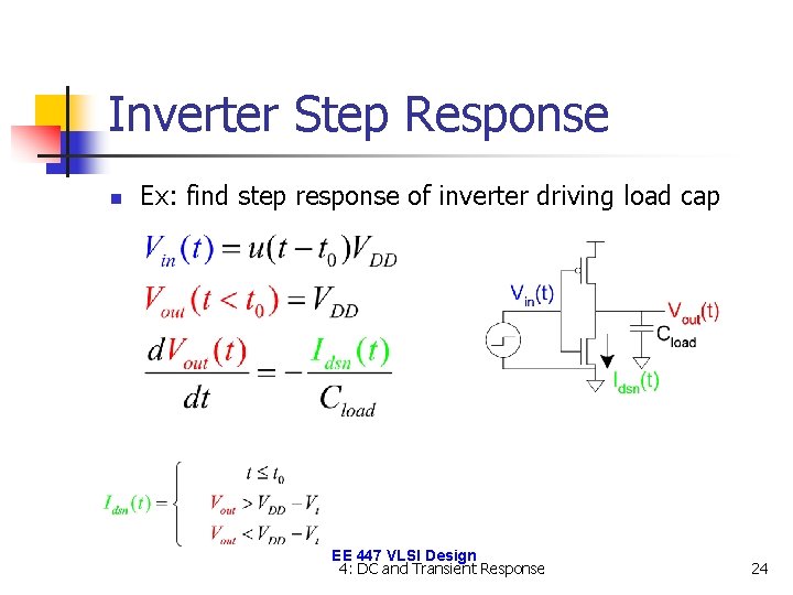
Transient Response n n DC analysis tells us Vout if Vin is constant Transient analysis tells us Vout(t) if Vin(t) changes n n Requires solving differential equations Input is usually considered to be a step or ramp n From 0 to VDD or vice versa EE 447 VLSI Design 4: DC and Transient Response 20

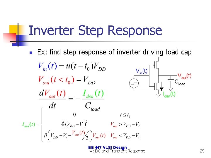
Inverter Step Response n Ex: find step response of inverter driving load cap EE 447 VLSI Design 4: DC and Transient Response 21

Inverter Step Response n Ex: find step response of inverter driving load cap EE 447 VLSI Design 4: DC and Transient Response 22

Inverter Step Response n Ex: find step response of inverter driving load cap EE 447 VLSI Design 4: DC and Transient Response 23

Inverter Step Response n Ex: find step response of inverter driving load cap EE 447 VLSI Design 4: DC and Transient Response 24

Inverter Step Response n Ex: find step response of inverter driving load cap EE 447 VLSI Design 4: DC and Transient Response 25

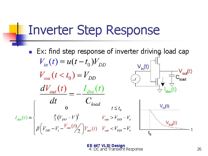
Inverter Step Response n Ex: find step response of inverter driving load cap EE 447 VLSI Design 4: DC and Transient Response 26

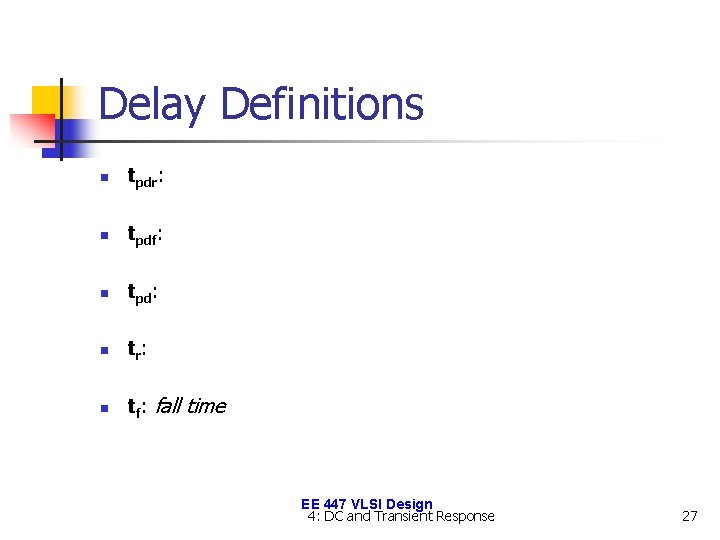
Delay Definitions n tpdr: n tpdf: n tpd: n tr : n tf: fall time EE 447 VLSI Design 4: DC and Transient Response 27

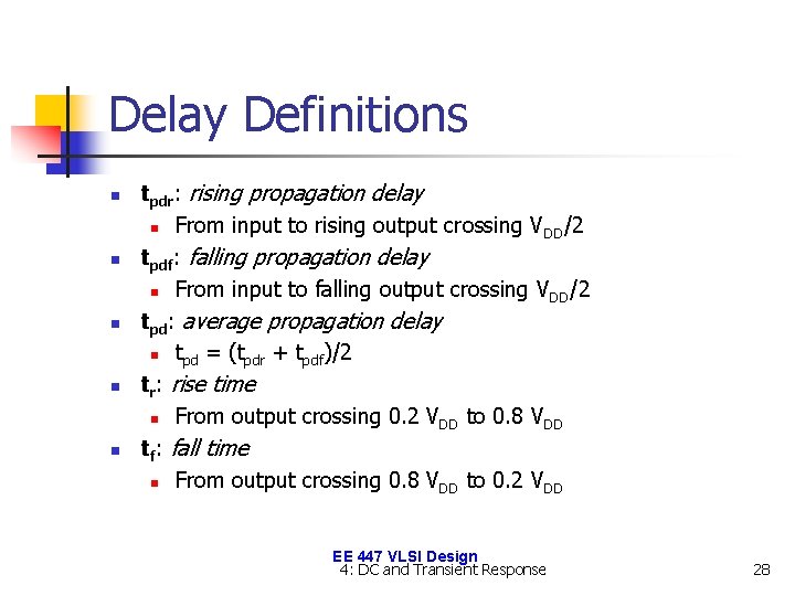
Delay Definitions n n n tpdr: rising propagation delay n From input to rising output crossing V DD/2 tpdf: falling propagation delay n From input to falling output crossing V DD/2 tpd: average propagation delay n tpd = (tpdr + tpdf)/2 tr: rise time n From output crossing 0. 2 VDD to 0. 8 VDD tf: fall time n From output crossing 0. 8 VDD to 0. 2 VDD EE 447 VLSI Design 4: DC and Transient Response 28

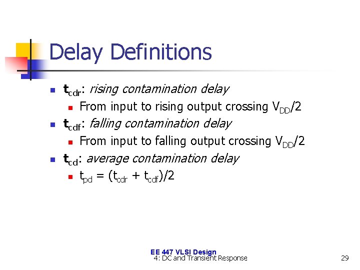
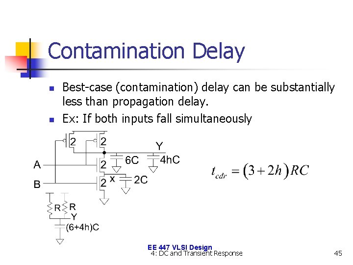
Delay Definitions n n n tcdr: rising contamination delay n From input to rising output crossing V DD/2 tcdf: falling contamination delay n From input to falling output crossing V DD/2 tcd: average contamination delay n tpd = (tcdr + tcdf)/2 EE 447 VLSI Design 4: DC and Transient Response 29

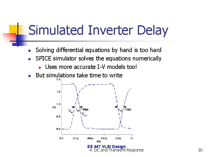
Simulated Inverter Delay n n n Solving differential equations by hand is too hard SPICE simulator solves the equations numerically n Uses more accurate I-V models too! But simulations take time to write EE 447 VLSI Design 4: DC and Transient Response 30

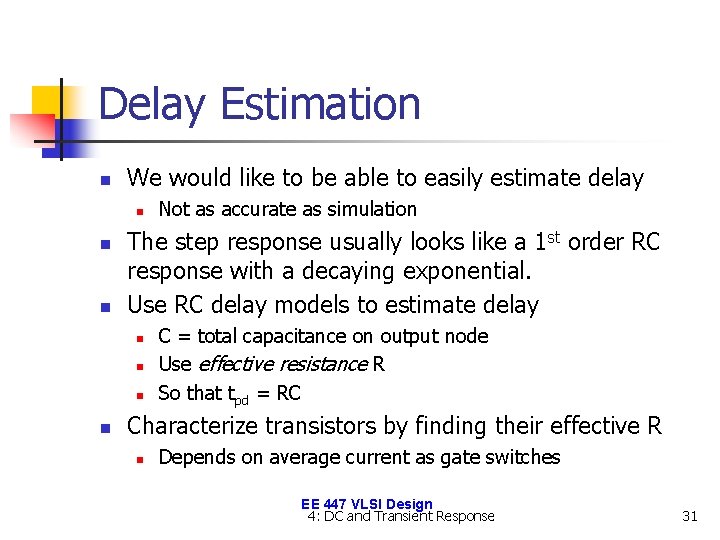
Delay Estimation n We would like to be able to easily estimate delay n n n The step response usually looks like a 1 st order RC response with a decaying exponential. Use RC delay models to estimate delay n n Not as accurate as simulation C = total capacitance on output node Use effective resistance R So that tpd = RC Characterize transistors by finding their effective R n Depends on average current as gate switches EE 447 VLSI Design 4: DC and Transient Response 31

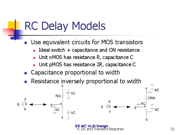
RC Delay Models n Use equivalent circuits for MOS transistors n n n Ideal switch + capacitance and ON resistance Unit n. MOS has resistance R, capacitance C Unit p. MOS has resistance 2 R, capacitance C Capacitance proportional to width Resistance inversely proportional to width EE 447 VLSI Design 4: DC and Transient Response 32

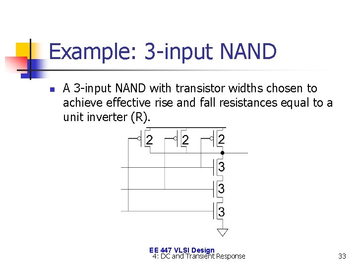
Example: 3 -input NAND n A 3 -input NAND with transistor widths chosen to achieve effective rise and fall resistances equal to a unit inverter (R). EE 447 VLSI Design 4: DC and Transient Response 33

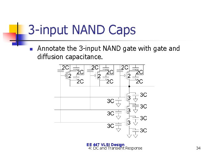
3 -input NAND Caps n Annotate the 3 -input NAND gate with gate and diffusion capacitance. EE 447 VLSI Design 4: DC and Transient Response 34

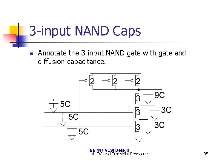
3 -input NAND Caps n Annotate the 3 -input NAND gate with gate and diffusion capacitance. EE 447 VLSI Design 4: DC and Transient Response 35

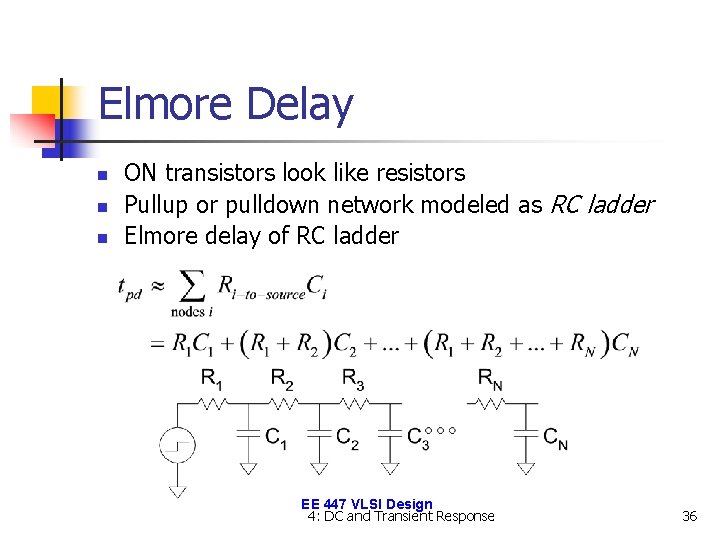
Elmore Delay n n n ON transistors look like resistors Pullup or pulldown network modeled as RC ladder Elmore delay of RC ladder EE 447 VLSI Design 4: DC and Transient Response 36

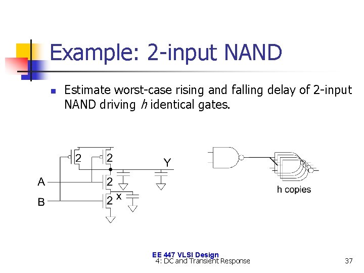
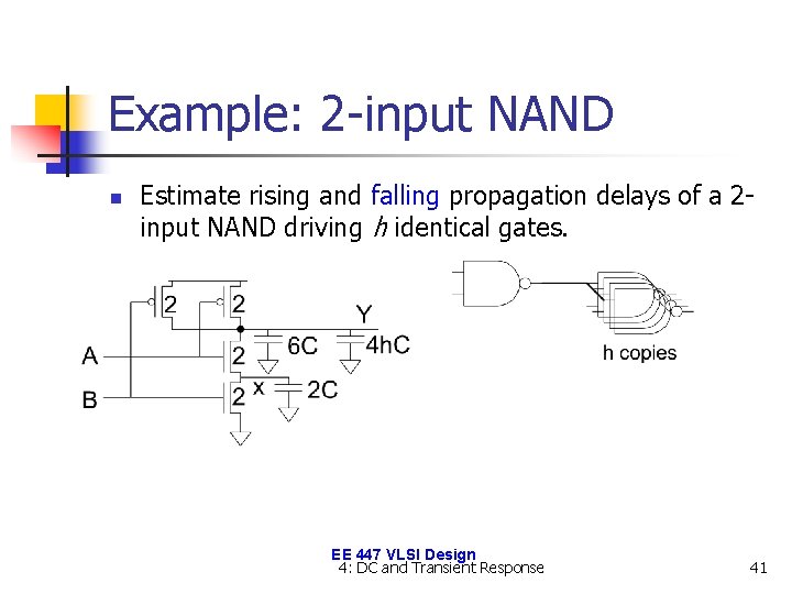
Example: 2 -input NAND n Estimate worst-case rising and falling delay of 2 -input NAND driving h identical gates. EE 447 VLSI Design 4: DC and Transient Response 37

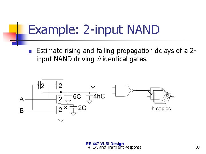
Example: 2 -input NAND n Estimate rising and falling propagation delays of a 2 input NAND driving h identical gates. EE 447 VLSI Design 4: DC and Transient Response 38

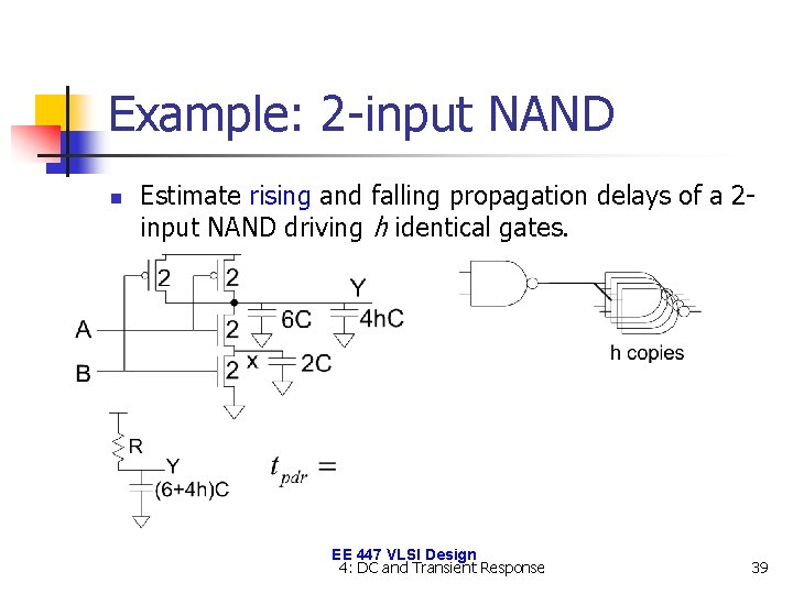
Example: 2 -input NAND n Estimate rising and falling propagation delays of a 2 input NAND driving h identical gates. EE 447 VLSI Design 4: DC and Transient Response 39

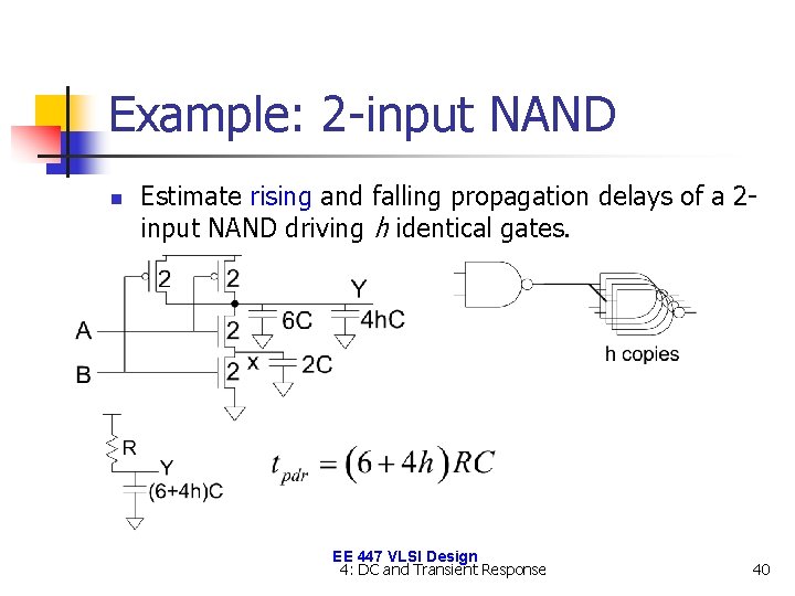
Example: 2 -input NAND n Estimate rising and falling propagation delays of a 2 input NAND driving h identical gates. EE 447 VLSI Design 4: DC and Transient Response 40

Example: 2 -input NAND n Estimate rising and falling propagation delays of a 2 input NAND driving h identical gates. EE 447 VLSI Design 4: DC and Transient Response 41

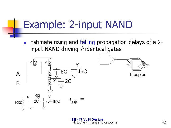
Example: 2 -input NAND n Estimate rising and falling propagation delays of a 2 input NAND driving h identical gates. EE 447 VLSI Design 4: DC and Transient Response 42

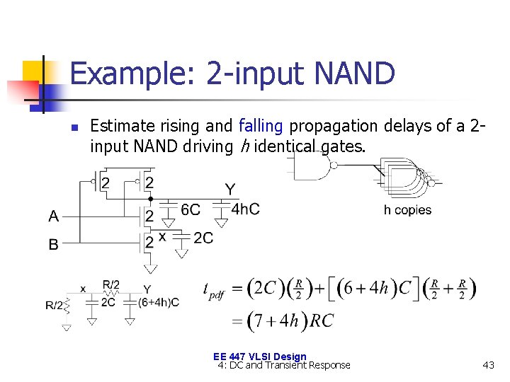
Example: 2 -input NAND n Estimate rising and falling propagation delays of a 2 input NAND driving h identical gates. EE 447 VLSI Design 4: DC and Transient Response 43

Delay Components n Delay has two parts n Parasitic delay n n n 6 or 7 RC Independent of load Effort delay n n 4 h RC Proportional to load capacitance EE 447 VLSI Design 4: DC and Transient Response 44

Contamination Delay n n Best-case (contamination) delay can be substantially less than propagation delay. Ex: If both inputs fall simultaneously EE 447 VLSI Design 4: DC and Transient Response 45

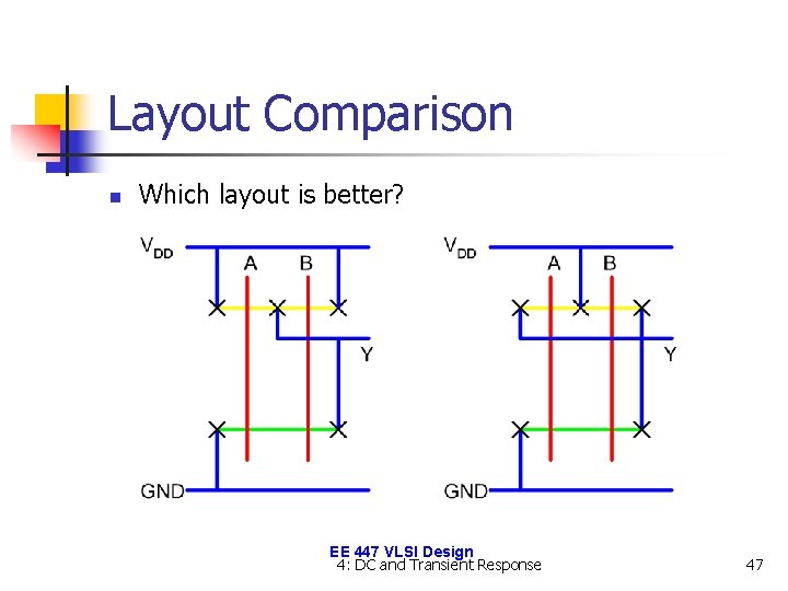
Diffusion Capacitance n n n we assumed contacted diffusion on every s / d. Good layout minimizes diffusion area Ex: NAND 3 layout shares one diffusion contact n n Reduces output capacitance by 2 C Merged uncontacted diffusion might help too EE 447 VLSI Design 4: DC and Transient Response 46

Layout Comparison n Which layout is better? EE 447 VLSI Design 4: DC and Transient Response 47