
Reducing Ripple and Transient Response 1 Output Caps



- Slides: 37
Reducing Ripple and Transient Response 1
Output Caps Selection The output capacitor must be designed to fulfill mainly two requirements: 1. To keep the steady-state peak-to-peak output voltage ripple below the maximum allowed value ∆Vopp 2. To keep the output voltage waveform within the required regulation window [Vo ± ∆Vo_reg] during the overshoot and undershoot caused by output current transients The output capacitor design of a buck converter will be discussed in this presentation 2 2
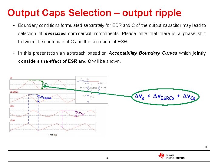
Output Caps Selection – output ripple • Boundary conditions formulated separately for ESR and C of the output capacitor may lead to selection of oversized commercial components. Please note that there is a phase shift between the contribute of C and the contribute of ESR. • In this presentation an approach based on Acceptability Boundary Curves which jointly considers the effect of ESR and C will be shown. 3 3
Output Caps Selection – stray inductances in output ripple analysis • Depending on the constant ESR x C, the output voltage waveform can change from quasi-triangular to quasi-sinusoidal. • The effect of stray inductances can be easily separated from the effect of the principal parameters ESR and C of the capacitor. In fact, stray inductances produce additive step-up and step-down effects on Dominant ESR the output voltage, whose amplitude is given by: Tantalum Electrolytic Dominant C Ceramic NO ESL Bad layout Includes ESL 4 4
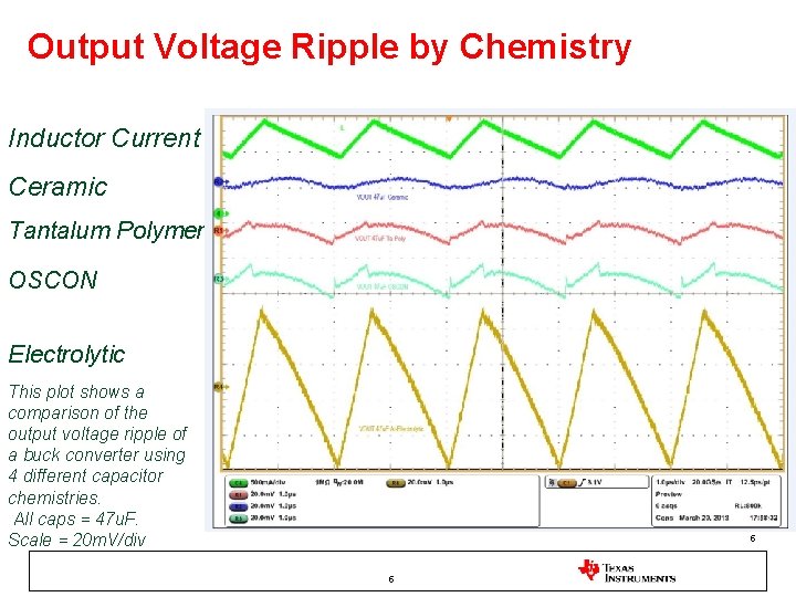
Output Voltage Ripple by Chemistry Inductor Current Ceramic Tantalum Polymer OSCON Electrolytic This plot shows a comparison of the output voltage ripple of a buck converter using 4 different capacitor chemistries. All caps = 47 u. F. Scale = 20 m. V/div 5 5
Output Caps Selection – stray inductances in output ripple analysis • In order to take in account the effect determined by the equivalent series inductance (ESL) of the output capacitor and by the inductance of the printed circuit board trace LPCB it is sufficient to replace the maximum allowed peak-to-peak output ripple voltage amplitude ΔVOpp with the net effective peak-to-peak ripple voltage ΔVOppeff allowed to ESR and capacitance C, given by: • If ESL and LPCB are unknown, the previous formula can also be used to determine the maximum allowed ESL compatible with the ESR and capacitance C of a capacitor selected with the algorithm not including the LPCB : 6 6
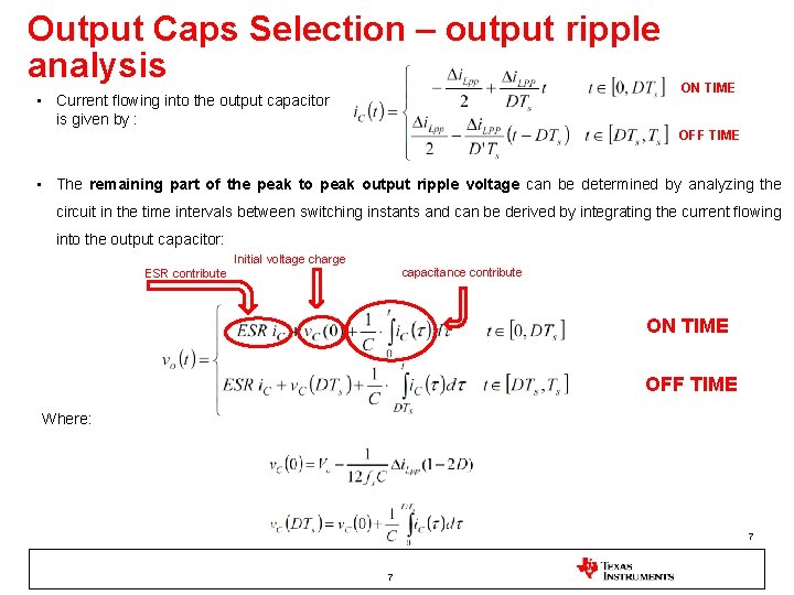
Output Caps Selection – output ripple analysis • Current flowing into the output capacitor is given by : ON TIME OFF TIME • The remaining part of the peak to peak output ripple voltage can be determined by analyzing the circuit in the time intervals between switching instants and can be derived by integrating the current flowing into the output capacitor: Initial voltage charge capacitance contribute ESR contribute ON TIME OFF TIME Where: 7 7
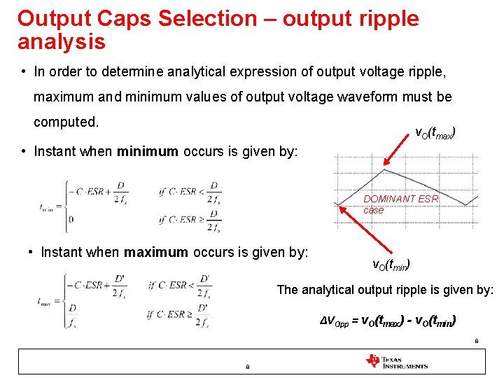
Output Caps Selection – output ripple analysis • In order to determine analytical expression of output voltage ripple, maximum and minimum values of output voltage waveform must be computed. v. O(tmax) • Instant when minimum occurs is given by: DOMINANT ESR case • Instant when maximum occurs is given by: v. O(tmin) The analytical output ripple is given by: ∆VOpp = v. O(tmax) - v. O(tmin) 8 8
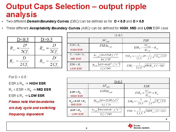
Output Caps Selection – output ripple analysis • Two different Domain Boundary Curves (DBC) can be defined as for D < 0. 5 and D > 0. 5 • Three different Acceptability Boundary Curves (ABC) can be defined for HIGH, MID and LOW ESR case HIGH ESR MID ESR LOW ESR For D < 0. 5 : ESR ≥ Rs- HIGH ESR Ri- < ESR < Rs- MID ESR ≤ Ri- LOW ESR Please note that boundaries are duty cycle and switching frequency dependent ESR > R+ s+ HIGH ESR Rs+< ESR < Ri+ MID ESR < Ri+ LOW ESR 9 9
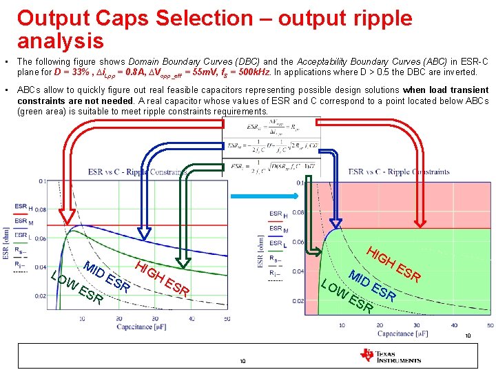
Output Caps Selection – output ripple analysis • The following figure shows Domain Boundary Curves (DBC) and the Acceptability Boundary Curves (ABC) in ESR-C plane for D = 33% , ∆i. Lpp = 0. 8 A, ∆Vopp_eff = 55 m. V, f. S = 500 k. Hz. In applications where D > 0. 5 the DBC are inverted. • ABCs allow to quickly figure out real feasible capacitors representing possible design solutions when load transient constraints are not needed. A real capacitor whose values of ESR and C correspond to a point located below ABCs (green area) is suitable to meet ripple constraints requirements. MI DE LO SR W ES R HIG HE HIG SR MI D LO ES W R ES R HE SR 10 10
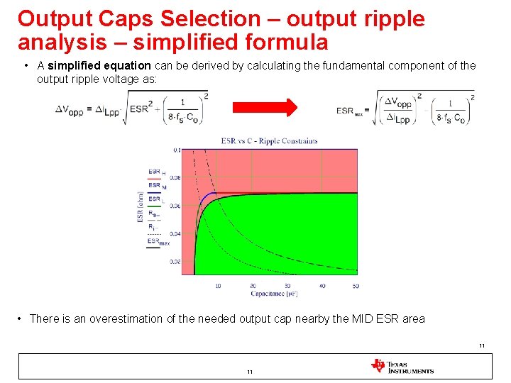
Output Caps Selection – output ripple analysis – simplified formula • A simplified equation can be derived by calculating the fundamental component of the output ripple voltage as: • There is an overestimation of the needed output cap nearby the MID ESR area 11 11
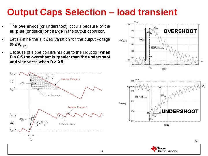
Output Caps Selection – load transient • The overshoot (or undershoot) occurs because of the surplus (or deficit) of charge in the output capacitor. • Let’s define the allowed variation for the output voltage as ∆Voreg • Because of slope constraints due to the inductor: when D < 0. 5 the overshoot is greater than the undershoot and vice versa when D > 0. 5 OVERSHOOT UNDERSHOOT 12 12
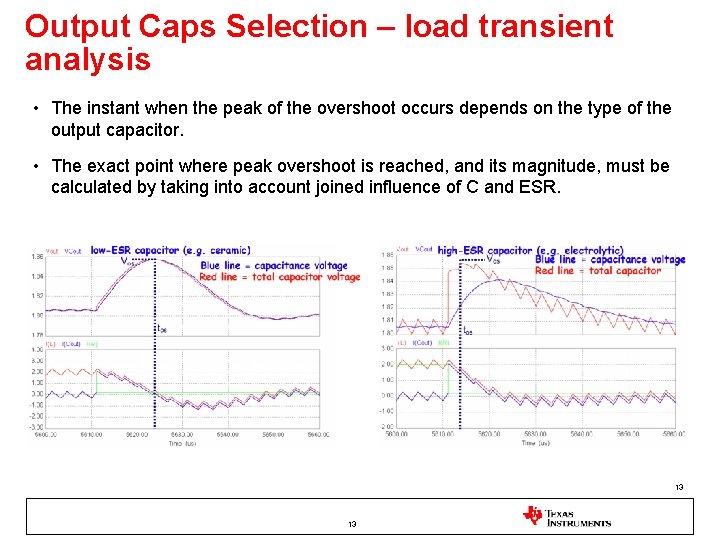
Output Caps Selection – load transient analysis • The instant when the peak of the overshoot occurs depends on the type of the output capacitor. • The exact point where peak overshoot is reached, and its magnitude, must be calculated by taking into account joined influence of C and ESR. 13 13
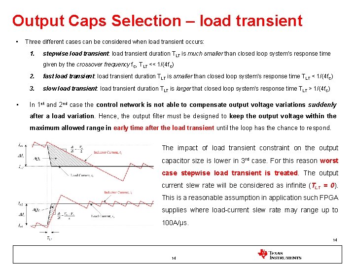
Output Caps Selection – load transient • Three different cases can be considered when load transient occurs: 1. stepwise load transient: load transient duration TLT is much smaller than closed loop system’s response time given by the crossover frequency f. C, TLT << 1/(4 f. C) • 2. fast load transient: load transient duration TLT is smaller than closed loop system’s response time TLT < 1/(4 f. C) 3. slow load transient: load transient duration TLT is larger that closed loop system’s response time TLT > 1/(4 f. C) In 1 st and 2 nd case the control network is not able to compensate output voltage variations suddenly after a load variation. Hence, the output filter must be designed to keep the output voltage within the maximum allowed range in early time after the load transient until the loop has the chance to respond. The impact of load transient constraint on the output capacitor size is lower in 3 rd case. For this reason worst case stepwise load transient is treated. The output current slew rate will be considered as infinite (TLT = 0). This is a reasonable assumption in application such FPGA supplies where load-current slew rate may range up to 100 A/µs. 14 14
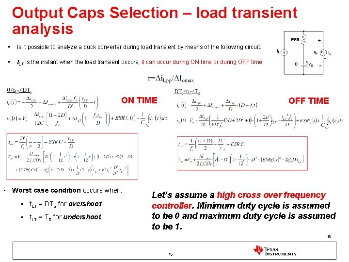
Output Caps Selection – load transient analysis • Is it possible to analyze a buck converter during load transient by means of the following circuit. • t. LT is the instant when the load transient occurs, it can occur during ON time or during OFF time. ON TIME • Worst case condition occurs when: • t. LT = DTS for overshoot • t. LT = TS for undershoot OFF TIME Let’s assume a high cross over frequency controller. Minimum duty cycle is assumed to be 0 and maximum duty cycle is assumed to be 1. 15 15
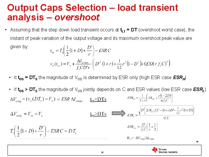
Output Caps Selection – load transient analysis – overshoot • Assuming that the step down load transient occurs at t. LT = DT (overshoot worst case), the instant of peak variation of the output voltage and its maximum overshoot peak value are given by: • It t. OS = DTS the magnitude of VOS is determined by ESR only (high ESR case ESRH) • If t. OS > DTS the magnitude of VOS jointly depends on C and ESR values (low ESR case ESRL) 16 16
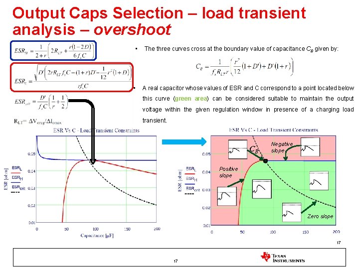
Output Caps Selection – load transient analysis – overshoot • • The three curves cross at the boundary value of capacitance CB given by: A real capacitor whose values of ESR and C correspond to a point located below this curve (green area) can be considered suitable to maintain the output voltage within the given regulation window in presence of a charging load transient. CB Negative slope Positive slope Zero slope 17 17
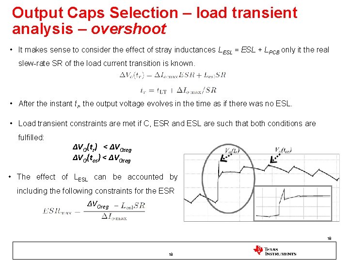
Output Caps Selection – load transient analysis – overshoot • It makes sense to consider the effect of stray inductances LESL = ESL + LPCB only it the real slew-rate SR of the load current transition is known. • After the instant tr, the output voltage evolves in the time as if there was no ESL. • Load transient constraints are met if C, ESR and ESL are such that both conditions are fulfilled: ∆VO(tr) < ∆VOreg ∆VO(tos) < ∆VOreg • The effect of LESL can be accounted by including the following constraints for the ESR ∆VOreg 18 18
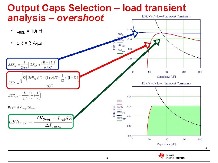
Output Caps Selection – load transient analysis – overshoot • LESL = 10 n. H • SR = 3 A/µs ∆VOreg 19 19
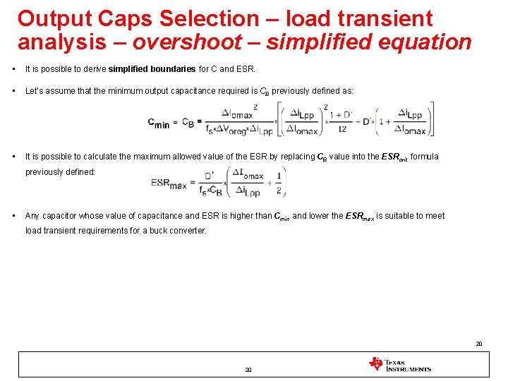
Output Caps Selection – load transient analysis – overshoot – simplified equation • It is possible to derive simplified boundaries for C and ESR. • Let’s assume that the minimum output capacitance required is CB previously defined as: • It is possible to calculate the maximum allowed value of the ESR by replacing CB value into the ESRcrit formula previously defined: • Any capacitor whose value of capacitance and ESR is higher than Cmin and lower the ESRmax is suitable to meet load transient requirements for a buck converter. 20 20
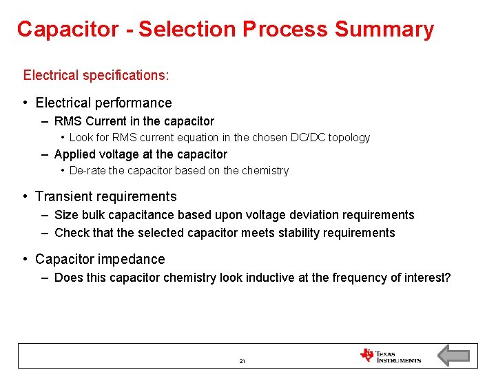
Capacitor - Selection Process Summary Electrical specifications: • Electrical performance – RMS Current in the capacitor • Look for RMS current equation in the chosen DC/DC topology – Applied voltage at the capacitor • De-rate the capacitor based on the chemistry • Transient requirements – Size bulk capacitance based upon voltage deviation requirements – Check that the selected capacitor meets stability requirements • Capacitor impedance – Does this capacitor chemistry look inductive at the frequency of interest? 21
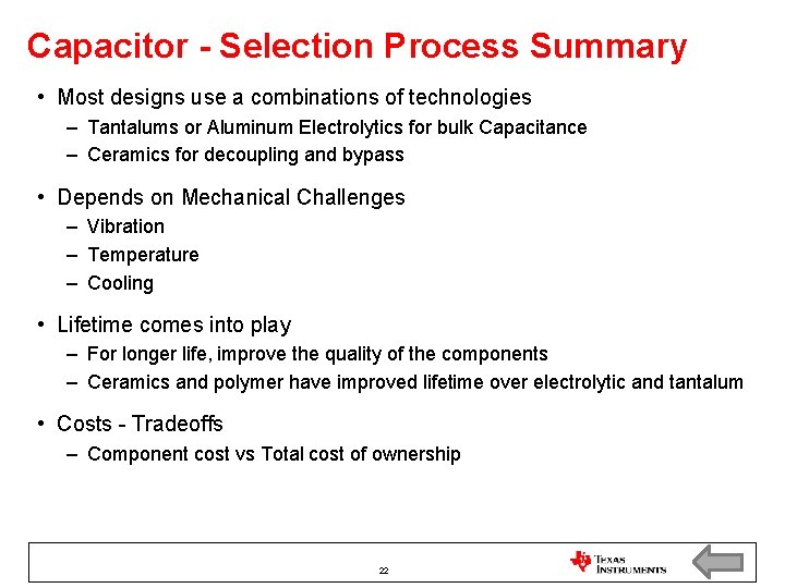
Capacitor - Selection Process Summary • Most designs use a combinations of technologies – Tantalums or Aluminum Electrolytics for bulk Capacitance – Ceramics for decoupling and bypass • Depends on Mechanical Challenges – Vibration – Temperature – Cooling • Lifetime comes into play – For longer life, improve the quality of the components – Ceramics and polymer have improved lifetime over electrolytic and tantalum • Costs - Tradeoffs – Component cost vs Total cost of ownership 22
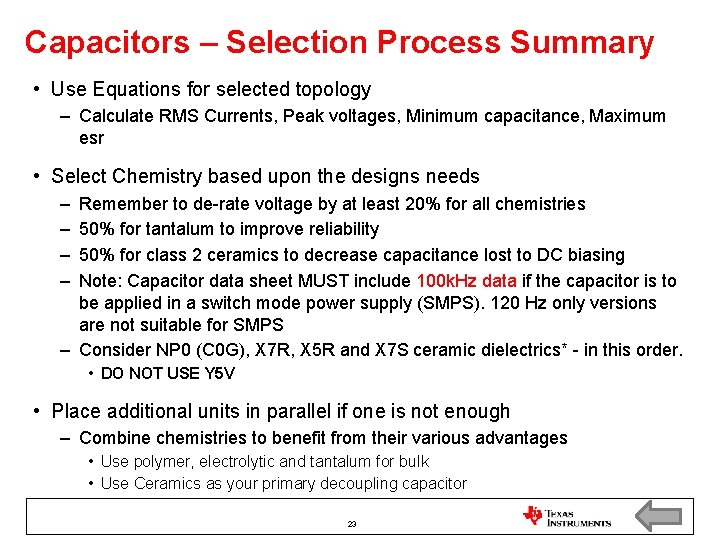
Capacitors – Selection Process Summary • Use Equations for selected topology – Calculate RMS Currents, Peak voltages, Minimum capacitance, Maximum esr • Select Chemistry based upon the designs needs – – Remember to de-rate voltage by at least 20% for all chemistries 50% for tantalum to improve reliability 50% for class 2 ceramics to decrease capacitance lost to DC biasing Note: Capacitor data sheet MUST include 100 k. Hz data if the capacitor is to be applied in a switch mode power supply (SMPS). 120 Hz only versions are not suitable for SMPS – Consider NP 0 (C 0 G), X 7 R, X 5 R and X 7 S ceramic dielectrics* - in this order. • DO NOT USE Y 5 V • Place additional units in parallel if one is not enough – Combine chemistries to benefit from their various advantages • Use polymer, electrolytic and tantalum for bulk • Use Ceramics as your primary decoupling capacitor 23
Output Caps Selection – References • A. De Nardo, N. Femia, G. Petrone, G. Spagnuolo, “A unified method for optimal buck converter output capacitor design”, Proc. Of ISIE 2008, Cambridge, UK, pp. 56 -61 • S. Maniktala, Switching Power Supply Design & Optimization, Mc Graw Hill, New York, 2004 • G. Spagnuolo, N. Femia, A. De Nardo, “Optimal Buck Converter Output Filter Design for Point of Load applications”, IEEE Trans. Ind. Electron. , DOI 10. 1109/TIE. 2009. 2030219, in press • R. W. Erickson, D. Maksimovic, “Fundamentals of Power Electronics”, 2001 Kluwer Academic Publishers 24 24
Paralleling capacitors to reduce high frequency output voltage ripple 25
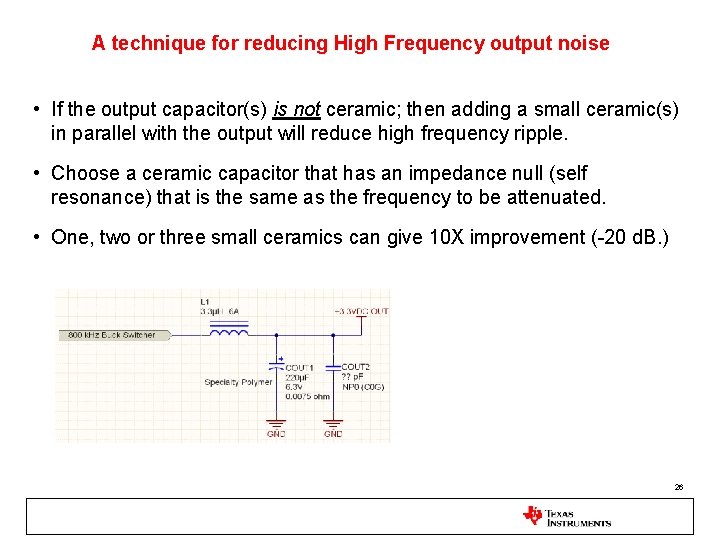
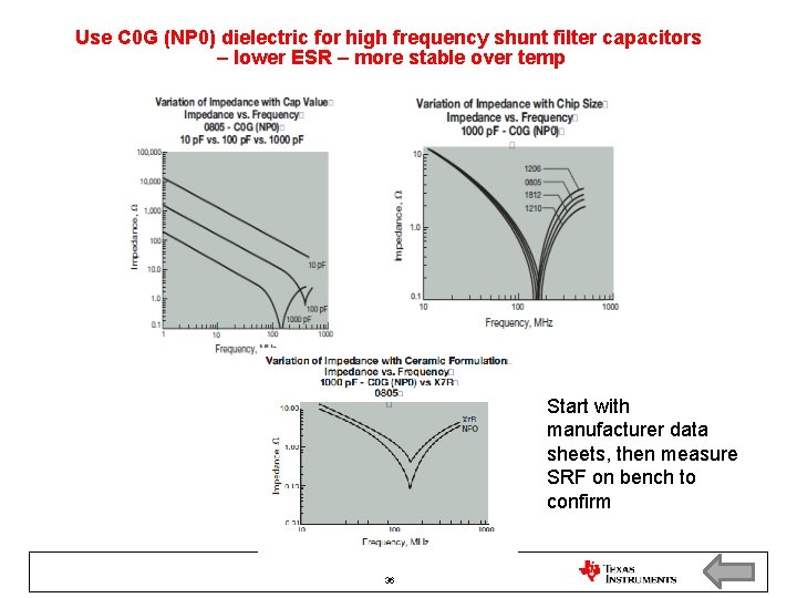
A technique for reducing High Frequency output noise • If the output capacitor(s) is not ceramic; then adding a small ceramic(s) in parallel with the output will reduce high frequency ripple. • Choose a ceramic capacitor that has an impedance null (self resonance) that is the same as the frequency to be attenuated. • One, two or three small ceramics can give 10 X improvement (-20 d. B. ) 26
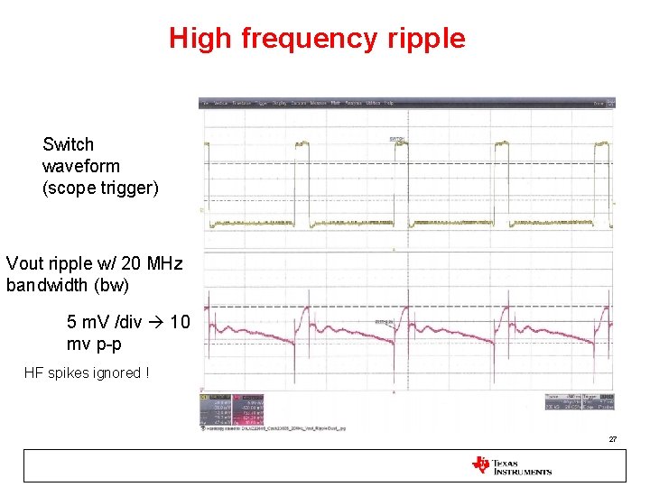
High frequency ripple Switch waveform (scope trigger) Vout ripple w/ 20 MHz bandwidth (bw) 5 m. V /div 10 mv p-p HF spikes ignored ! 27
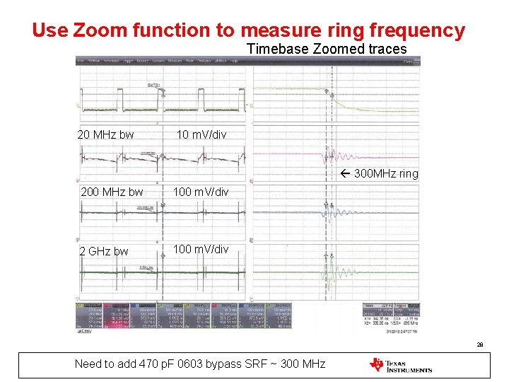
Use Zoom function to measure ring frequency Timebase Zoomed traces 20 MHz bw 10 m. V/div 300 MHz ring 200 MHz bw 100 m. V/div 2 GHz bw 100 m. V/div 28 Need to add 470 p. F 0603 bypass SRF ~ 300 MHz
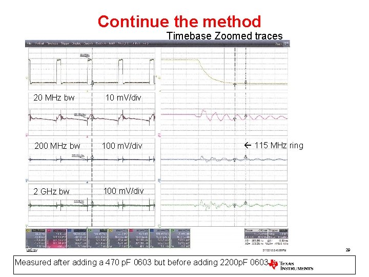
Continue the method Timebase Zoomed traces 20 MHz bw 10 m. V/div 200 MHz bw 100 m. V/div 2 GHz bw 100 m. V/div 115 MHz ring 29 Measured after adding a 470 p. F 0603 but before adding 2200 p. F 0603
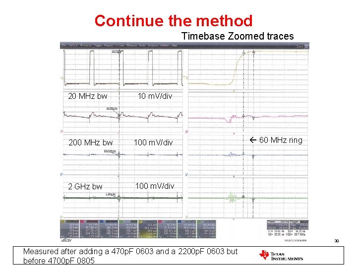
Continue the method Timebase Zoomed traces 20 MHz bw 10 m. V/div 200 MHz bw 100 m. V/div 2 GHz bw 100 m. V/div 60 MHz ring 30 Measured after adding a 470 p. F 0603 and a 2200 p. F 0603 but before 4700 p. F 0805
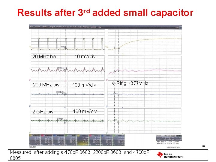
Results after 3 rd added small capacitor 20 MHz bw 10 m. V/div 200 MHz bw 100 m. V/div 2 GHz bw 100 m. V/div Ring ~377 MHz 31 Measured after adding a 470 p. F 0603, 2200 p. F 0603, and 4700 p. F 0805
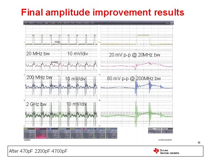
Final amplitude improvement results 20 MHz bw 10 m. V/div 200 MHz bw 10 m. V/div 2 GHz bw 10 m. V/div 20 m. V p-p @ 20 MHz bw 80 m. V p-p @ 200 MHz bw 32 After 470 p. F 2200 p. F 4700 p. F
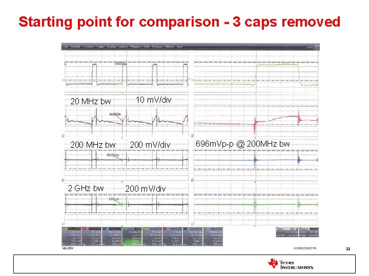
Starting point for comparison - 3 caps removed 20 MHz bw 200 MHz bw 2 GHz bw 10 m. V/div 200 m. V/div 696 m. Vp-p @ 200 MHz bw 200 m. V/div 33
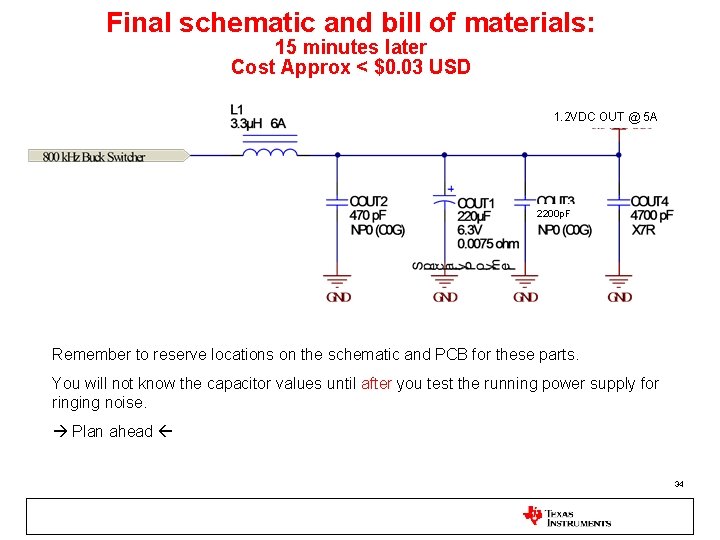
Final schematic and bill of materials: 15 minutes later Cost Approx < $0. 03 USD 1. 2 VDC OUT @ 5 A 2200 p. F Remember to reserve locations on the schematic and PCB for these parts. You will not know the capacitor values until after you test the running power supply for ringing noise. Plan ahead 34
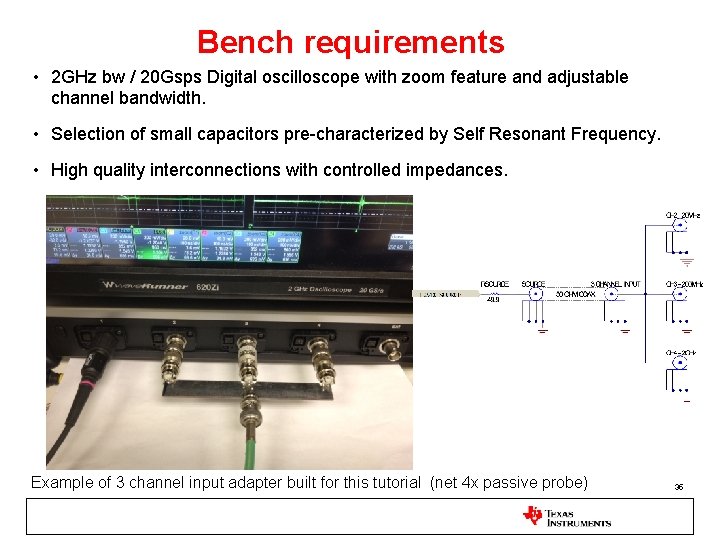
Bench requirements • 2 GHz bw / 20 Gsps Digital oscilloscope with zoom feature and adjustable channel bandwidth. • Selection of small capacitors pre-characterized by Self Resonant Frequency. • High quality interconnections with controlled impedances. Example of 3 channel input adapter built for this tutorial (net 4 x passive probe) 35
Use C 0 G (NP 0) dielectric for high frequency shunt filter capacitors – lower ESR – more stable over temp Start with manufacturer data sheets, then measure SRF on bench to confirm 36
Thank You Questions? 37