
VLSI System Design Lect 2 2 CMOS Transistor
- Slides: 33
VLSI System Design Lect. 2. 2 CMOS Transistor Theory 2 Engr. Anees ul Husnain ( anees. buzdar@gmail. com ) Department of Electronics & Computer Systems Engineering, College of Engineering & Technology, IUB
Outline. . . o Non-ideal Transistor Behavior n High Field Effects o Mobility Degradation o Velocity Saturation n Channel Length Modulation
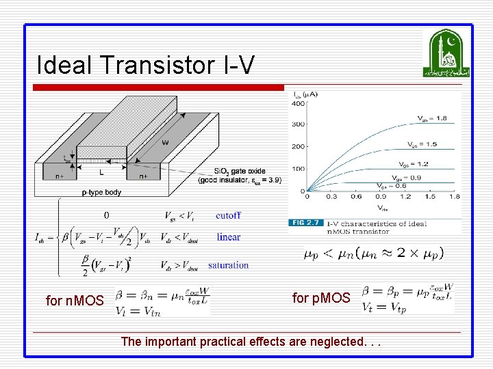
Ideal Transistor I-V for n. MOS for p. MOS The important practical effects are neglected. . .
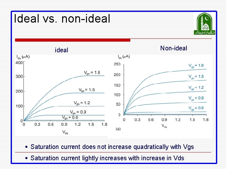
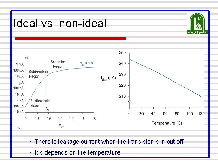
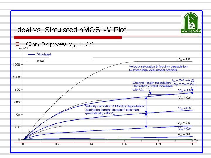
Ideal vs. non-ideal Non-ideal § Saturation current does not increase quadratically with Vgs § Saturation current lightly increases with increase in Vds
REASONS § Velocity Saturation § Mobility Degradation § Channel Length Modulation § Sub-Threshold Conduction § Junction Leakage
Ideal vs. non-ideal § There is leakage current when the transistor is in cut off § Ids depends on the temperature
Ideal vs. Simulated n. MOS I-V Plot o 65 nm IBM process, VDD = 1. 0 V
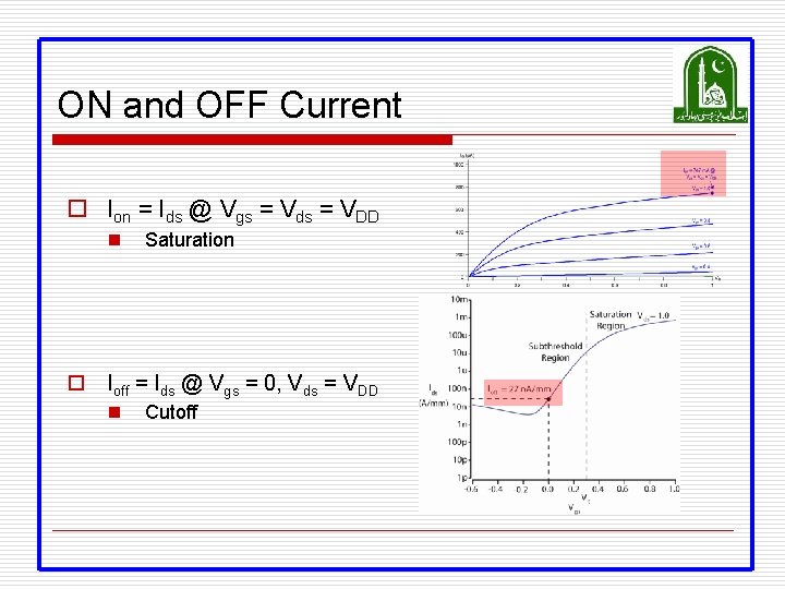
ON and OFF Current o Ion = Ids @ Vgs = Vds = VDD n Saturation o Ioff = Ids @ Vgs = 0, Vds = VDD n Cutoff
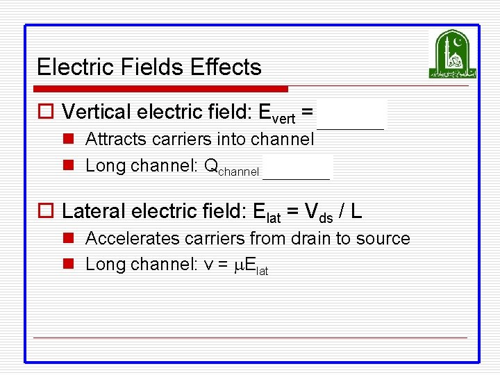
Electric Fields Effects o Vertical electric field: Evert = Vgs / tox n Attracts carriers into channel n Long channel: Qchannel Evert o Lateral electric field: Elat = Vds / L n Accelerates carriers from drain to source n Long channel: v = m. Elat
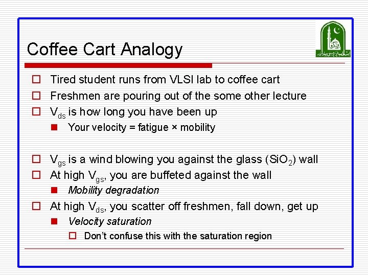
Coffee Cart Analogy o Tired student runs from VLSI lab to coffee cart o Freshmen are pouring out of the some other lecture o Vds is how long you have been up n Your velocity = fatigue × mobility o Vgs is a wind blowing you against the glass (Si. O 2) wall o At high Vgs, you are buffeted against the wall n Mobility degradation o At high Vds, you scatter off freshmen, fall down, get up n Velocity saturation o Don’t confuse this with the saturation region
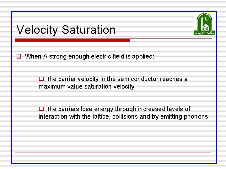
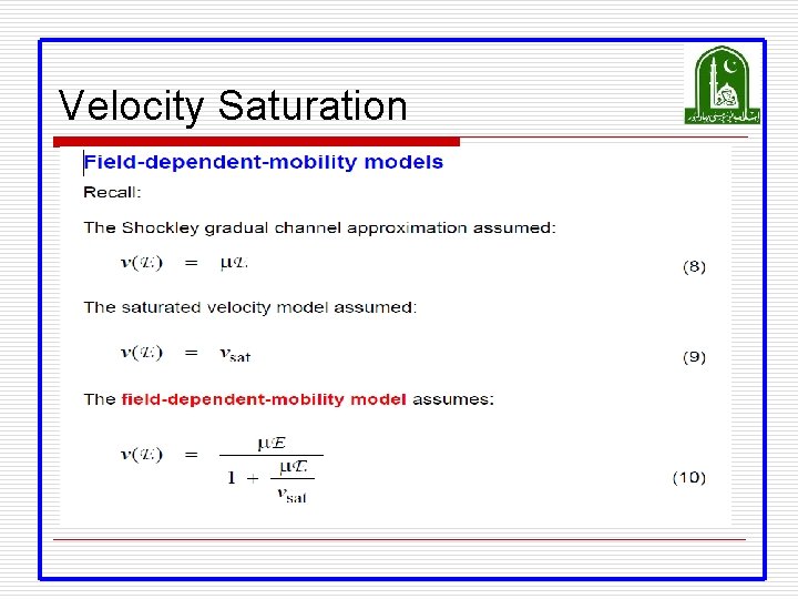
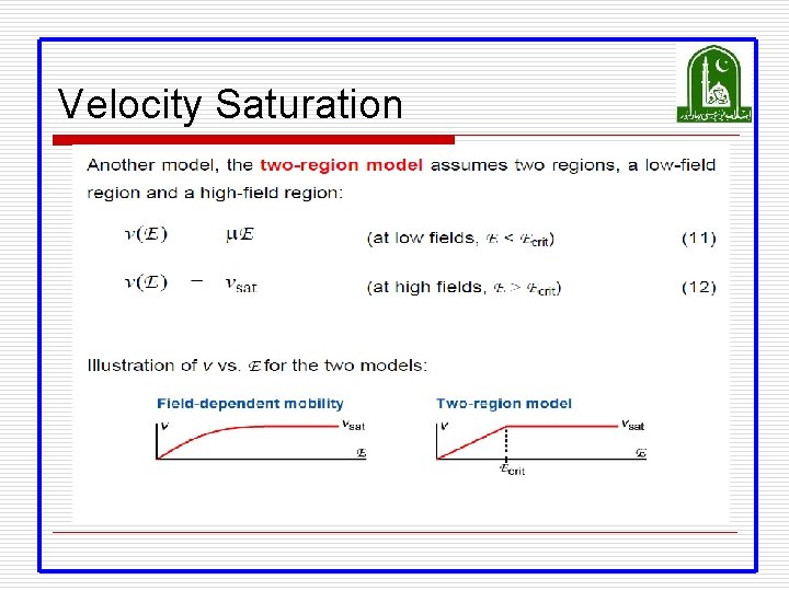
Velocity Saturation q When A strong enough electric field is applied: q the carrier velocity in the semiconductor reaches a maximum value saturation velocity q the carriers lose energy through increased levels of interaction with the lattice, collisions and by emitting phonons
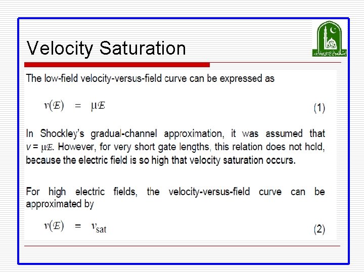
Velocity Saturation
Velocity Saturation
Velocity Saturation
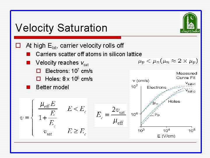
Velocity Saturation o At high Elat, carrier velocity rolls off n Carriers scatter off atoms in silicon lattice n Velocity reaches vsat o Electrons: 107 cm/s o Holes: 8 x 106 cm/s n Better model
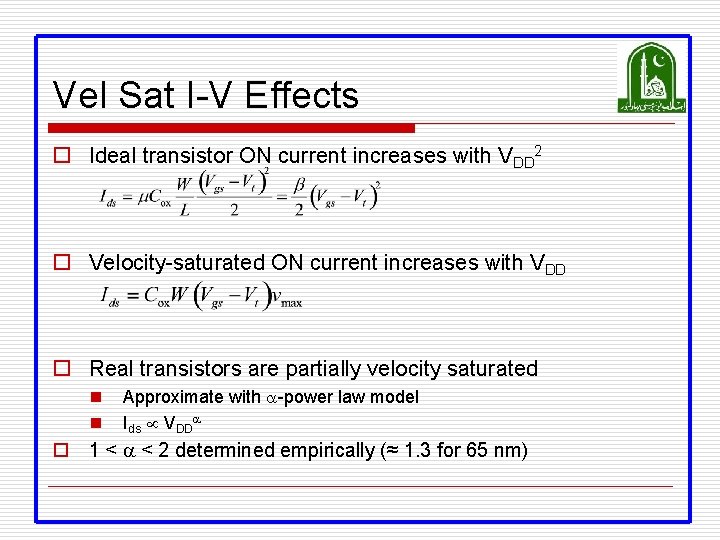
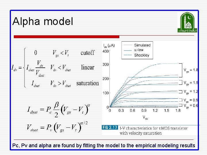
Vel Sat I-V Effects o Ideal transistor ON current increases with VDD 2 o Velocity-saturated ON current increases with VDD o Real transistors are partially velocity saturated n n Approximate with a-power law model Ids VDDa o 1 < a < 2 determined empirically (≈ 1. 3 for 65 nm)
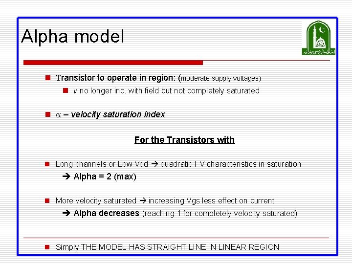
Alpha model n Transistor to operate in region: (moderate supply voltages) n v no longer inc. with field but not completely saturated n a – velocity saturation index For the Transistors with n Long channels or Low Vdd quadratic I-V characteristics in saturation Alpha = 2 (max) n More velocity saturated increasing Vgs less effect on current Alpha decreases (reaching 1 for completely velocity saturated) n Simply THE MODEL HAS STRAIGHT LINE IN LINEAR REGION
Alpha model Pc, Pv and alpha are found by fitting the model to the empirical modeling results
Empirical Modeling o Refers to any kind of (computer) modelling based on empirical observations rather than on mathematically describable relationships of the system modelled. o The word empirical denotes information gained by means of observation, experience, or experiment
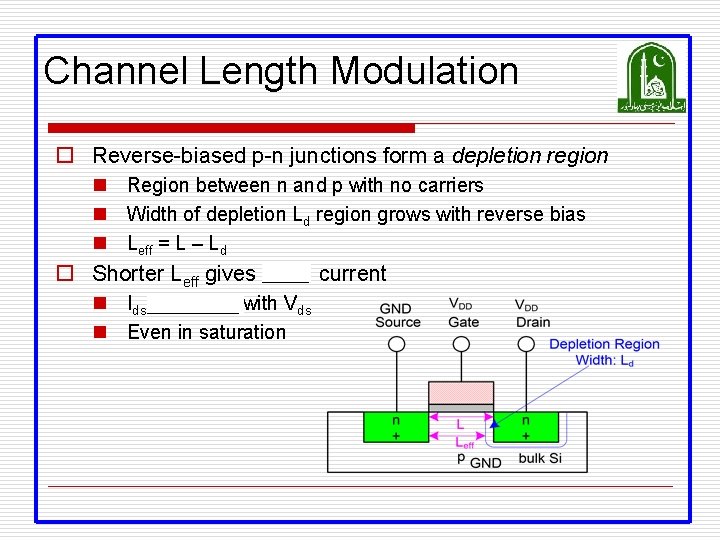
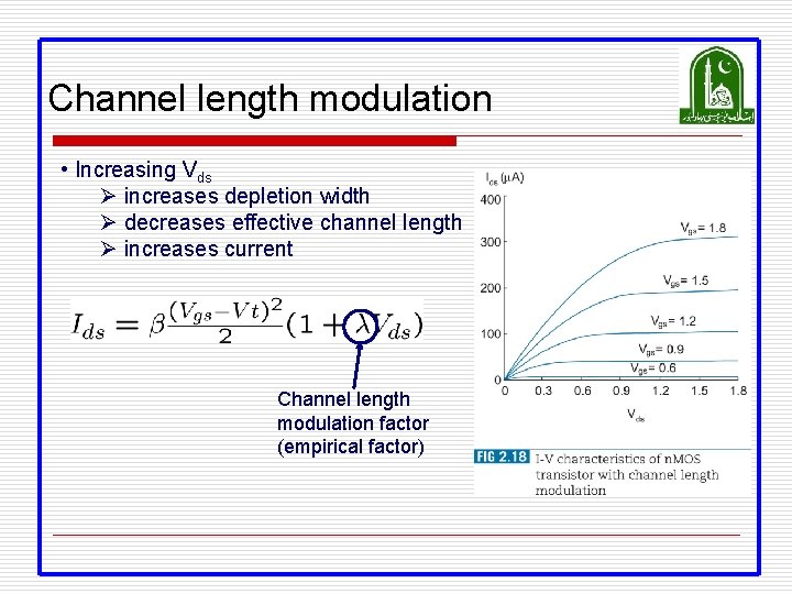
Channel Length Modulation o Reverse-biased p-n junctions form a depletion region n Region between n and p with no carriers n Width of depletion Ld region grows with reverse bias n Leff = L – Ld o Shorter Leff gives more current n Ids increases with Vds n Even in saturation
Channel length modulation • Increasing Vds Ø increases depletion width Ø decreases effective channel length Ø increases current Channel length modulation factor (empirical factor)
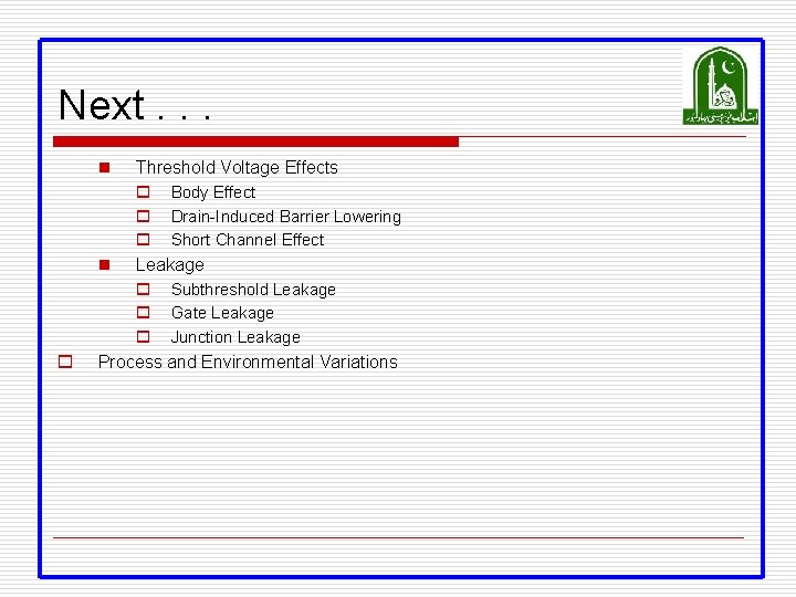
Next. . . n o Threshold Voltage Effects o Body Effect o Drain-Induced Barrier Lowering o Short Channel Effect n Leakage o Subthreshold Leakage o Gate Leakage o Junction Leakage Process and Environmental Variations
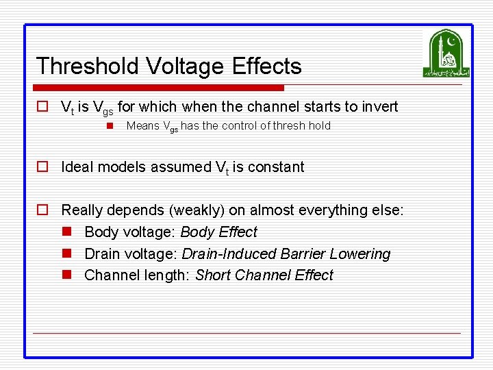
Threshold Voltage Effects o Vt is Vgs for which when the channel starts to invert n Means Vgs has the control of thresh hold o Ideal models assumed Vt is constant o Really depends (weakly) on almost everything else: n Body voltage: Body Effect n Drain voltage: Drain-Induced Barrier Lowering n Channel length: Short Channel Effect
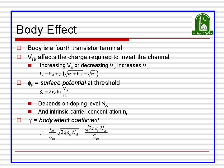
Body Effect o Body is a fourth transistor terminal o Vsb affects the charge required to invert the channel n Increasing Vs or decreasing Vb increases Vt o fs = surface potential at threshold n n o Depends on doping level NA And intrinsic carrier concentration ni g = body effect coefficient
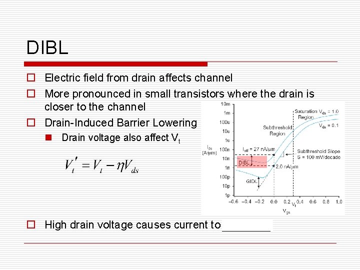
DIBL o Electric field from drain affects channel o More pronounced in small transistors where the drain is closer to the channel o Drain-Induced Barrier Lowering n Drain voltage also affect Vt o High drain voltage causes current to increase.
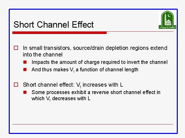
Short Channel Effect o In small transistors, source/drain depletion regions extend into the channel n Impacts the amount of charge required to invert the channel n And thus makes Vt a function of channel length o Short channel effect: Vt increases with L n Some processes exhibit a reverse short channel effect in which Vt decreases with L
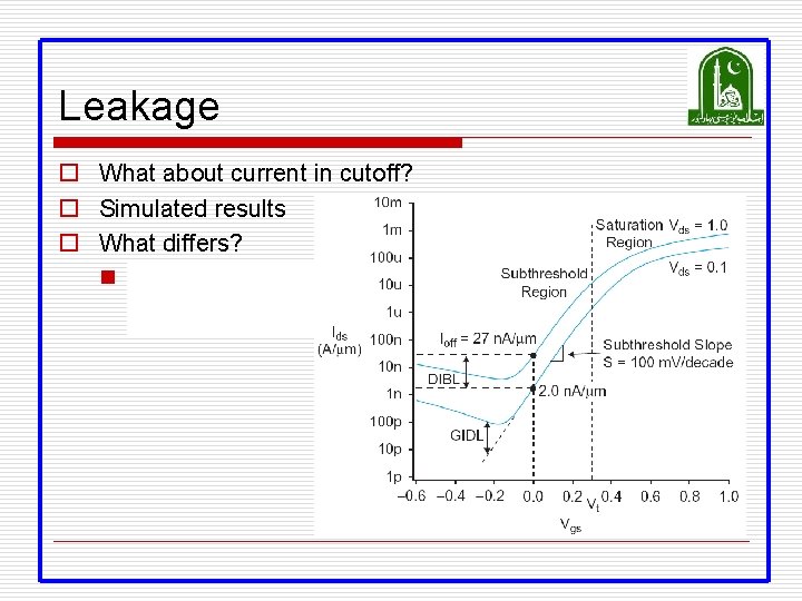
Leakage o What about current in cutoff? o Simulated results o What differs? n Current doesn’t go to 0 in cutoff
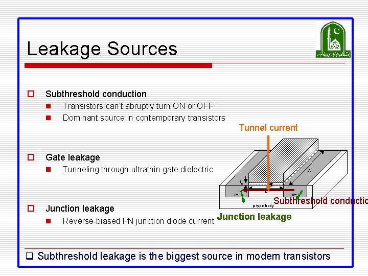
Leakage Sources o Subthreshold conduction n n Transistors can’t abruptly turn ON or OFF Dominant source in contemporary transistors Tunnel current o Gate leakage n polysilicon gate Tunneling through ultrathin gate dielectric W t ox n+ o Junction leakage n L n+ Subthreshold conductio p-type body Reverse-biased PN junction diode current Junction leakage q Subthreshold leakage is the biggest source in modern transistors
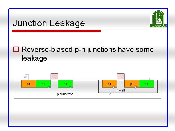
Junction Leakage o Reverse-biased p-n junctions have some leakage
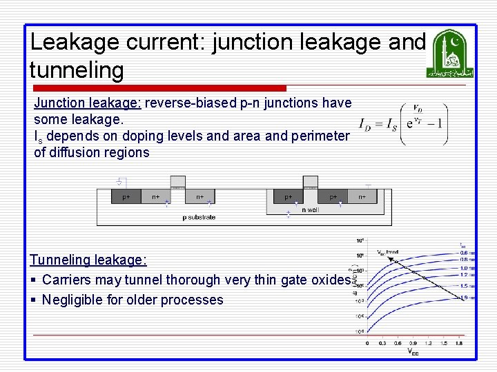
Leakage current: junction leakage and tunneling Junction leakage: reverse-biased p-n junctions have some leakage. Is depends on doping levels and area and perimeter of diffusion regions Tunneling leakage: § Carriers may tunnel thorough very thin gate oxides § Negligible for older processes
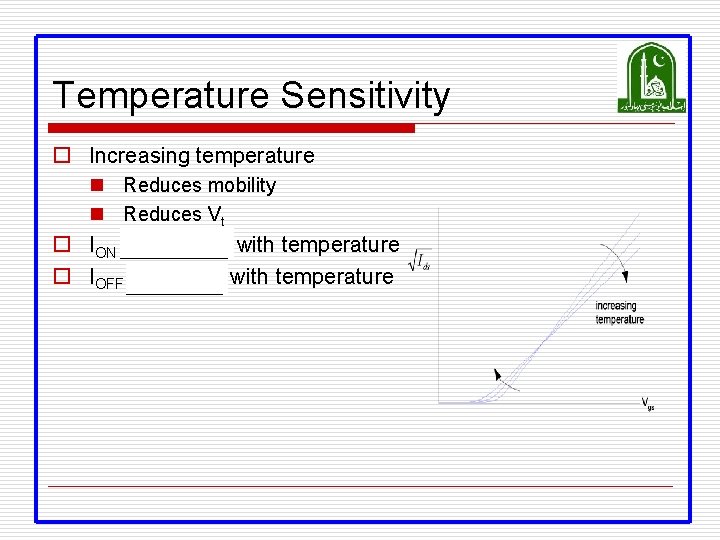
Temperature Sensitivity o Increasing temperature n Reduces mobility n Reduces Vt o ION decreases with temperature o IOFF increases with temperature
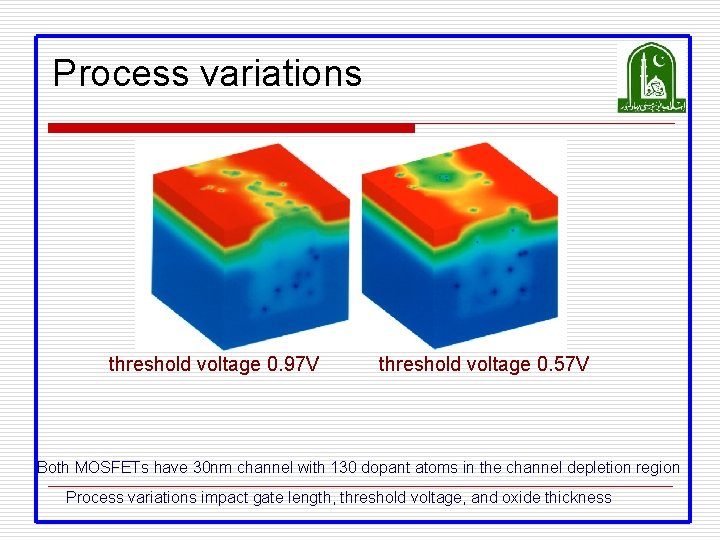
Process variations threshold voltage 0. 97 V threshold voltage 0. 57 V Both MOSFETs have 30 nm channel with 130 dopant atoms in the channel depletion region Process variations impact gate length, threshold voltage, and oxide thickness
So What? o So what if transistors are not ideal? n They still behave like switches. o But these effects matter for… n n n Supply voltage choice Logical effort Quiescent power consumption Pass transistors Temperature of operation