VLSI Design Lecture 5 Logic Gates Mohammad Arjomand

![AOI example out = [ab+c]’: invert symbol circuit or and Modern VLSI Design 4 AOI example out = [ab+c]’: invert symbol circuit or and Modern VLSI Design 4](https://slidetodoc.com/presentation_image/0f0bcac95dc9251381adfe4a6b06afb5/image-16.jpg)
- Slides: 43

VLSI Design Lecture 5: Logic Gates Mohammad Arjomand CE Department Sharif Univ. of Tech. Adapted with modifications from Wayne Wolf’s lecture notes

Topics Combinational logic functions. n Static complementary logic gate structures. n Modern VLSI Design 4 e: Chapter 3 Copyright 2008 Wayne Wolf

Combinational logic expressions Combinational logic: function value is a combination of function arguments. n A logic gate implements a particular logic function. n Both specification (logic equations) and implementation (logic gate networks) are written in Boolean logic. n Modern VLSI Design 4 e: Chapter 3 Copyright 2008 Wayne Wolf

Gate design Why designing gates for logic functions is non -trivial: – may not have logic gates in the libray for all logic expressions; – a logic expression may map into gates that consume a lot of area, delay, or power. Modern VLSI Design 4 e: Chapter 3 Copyright 2008 Wayne Wolf

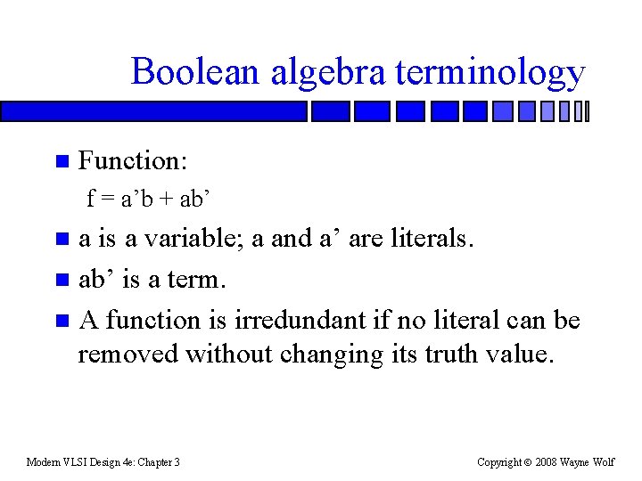
Boolean algebra terminology n Function: f = a’b + ab’ a is a variable; a and a’ are literals. n ab’ is a term. n A function is irredundant if no literal can be removed without changing its truth value. n Modern VLSI Design 4 e: Chapter 3 Copyright 2008 Wayne Wolf

Completeness A set of functions f 1, f 2, . . . is complete iff every Boolean function can be generated by a combination of the functions. n NAND is a complete set; NOR is a complete set; {AND, OR} is not complete. n Transmission gates are not complete. n If your set of logic gates is not complete, you can’t design arbitrary logic. n Modern VLSI Design 4 e: Chapter 3 Copyright 2008 Wayne Wolf

Static complementary gates Complementary: have complementary pullup (p-type) and pulldown (n-type) networks. n Static: do not rely on stored charge. n Simple, effective, reliable; hence ubiquitous. n Modern VLSI Design 4 e: Chapter 3 Copyright 2008 Wayne Wolf

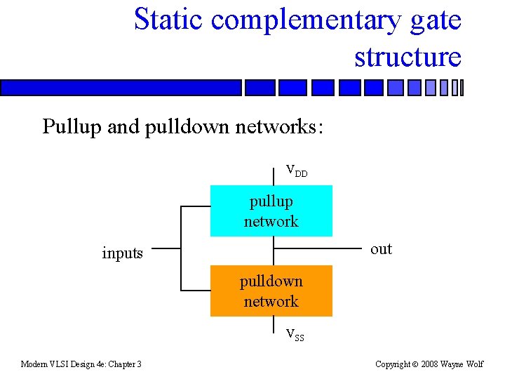
Static complementary gate structure Pullup and pulldown networks: VDD pullup network out inputs pulldown network VSS Modern VLSI Design 4 e: Chapter 3 Copyright 2008 Wayne Wolf

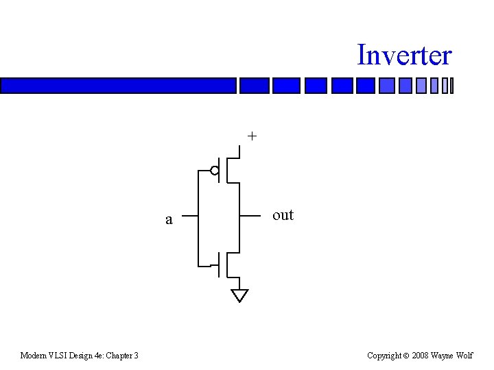
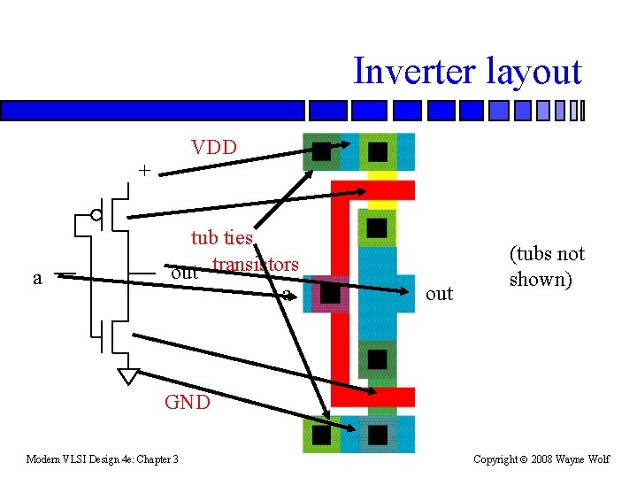
Inverter + a Modern VLSI Design 4 e: Chapter 3 out Copyright 2008 Wayne Wolf

Inverter layout VDD + a tub ties out transistors a out (tubs not shown) GND Modern VLSI Design 4 e: Chapter 3 Copyright 2008 Wayne Wolf

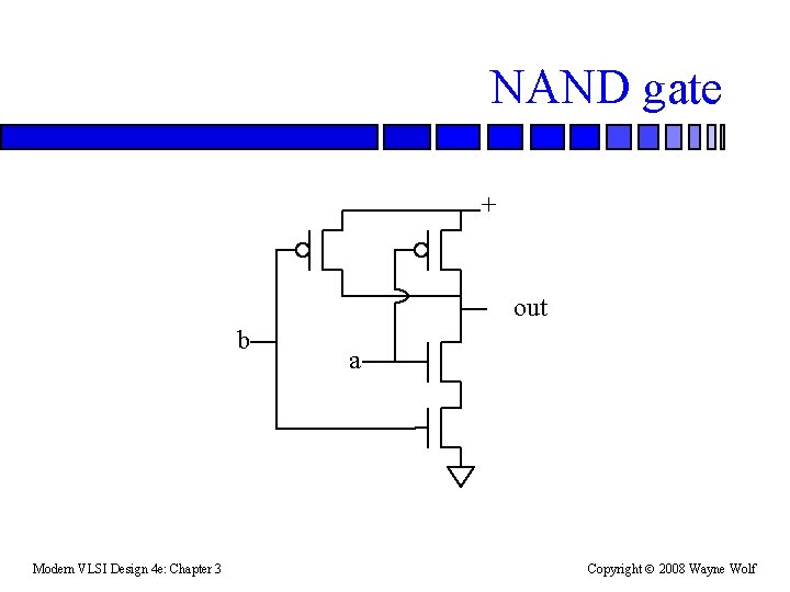
NAND gate + out b Modern VLSI Design 4 e: Chapter 3 a Copyright 2008 Wayne Wolf

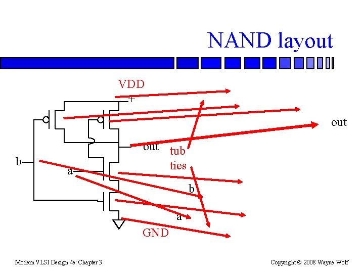
NAND layout VDD + out b a out tub ties b a GND Modern VLSI Design 4 e: Chapter 3 Copyright 2008 Wayne Wolf

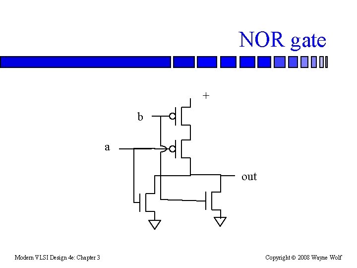
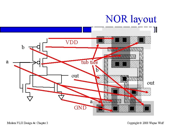
NOR gate + b a out Modern VLSI Design 4 e: Chapter 3 Copyright 2008 Wayne Wolf

NOR layout b VDD a out tub ties b out a GND Modern VLSI Design 4 e: Chapter 3 Copyright 2008 Wayne Wolf

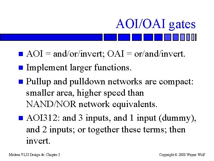
AOI/OAI gates AOI = and/or/invert; OAI = or/and/invert. n Implement larger functions. n Pullup and pulldown networks are compact: smaller area, higher speed than NAND/NOR network equivalents. n AOI 312: and 3 inputs, and 1 input (dummy), and 2 inputs; or together these terms; then invert. n Modern VLSI Design 4 e: Chapter 3 Copyright 2008 Wayne Wolf
![AOI example out abc invert symbol circuit or and Modern VLSI Design 4 AOI example out = [ab+c]’: invert symbol circuit or and Modern VLSI Design 4](https://slidetodoc.com/presentation_image/0f0bcac95dc9251381adfe4a6b06afb5/image-16.jpg)
AOI example out = [ab+c]’: invert symbol circuit or and Modern VLSI Design 4 e: Chapter 3 Copyright 2008 Wayne Wolf

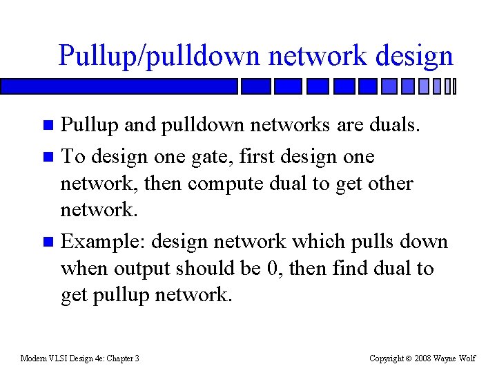
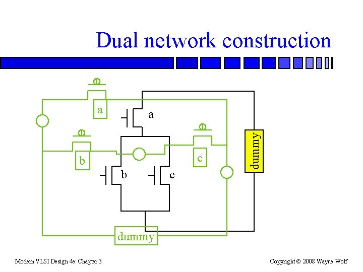
Pullup/pulldown network design Pullup and pulldown networks are duals. n To design one gate, first design one network, then compute dual to get other network. n Example: design network which pulls down when output should be 0, then find dual to get pullup network. n Modern VLSI Design 4 e: Chapter 3 Copyright 2008 Wayne Wolf

Dual network construction a c b b c dummy a dummy Modern VLSI Design 4 e: Chapter 3 Copyright 2008 Wayne Wolf

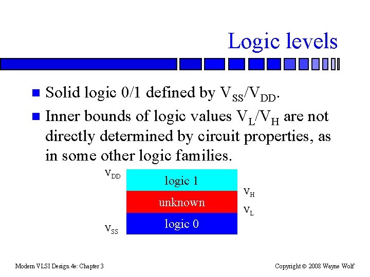
Logic levels Solid logic 0/1 defined by VSS/VDD. n Inner bounds of logic values VL/VH are not directly determined by circuit properties, as in some other logic families. n VDD logic 1 unknown VSS Modern VLSI Design 4 e: Chapter 3 VH VL logic 0 Copyright 2008 Wayne Wolf

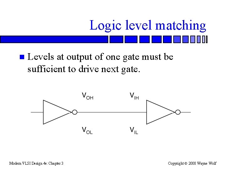
Logic level matching n Levels at output of one gate must be sufficient to drive next gate. Modern VLSI Design 4 e: Chapter 3 Copyright 2008 Wayne Wolf

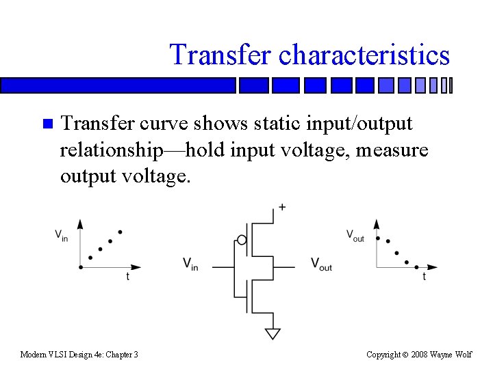
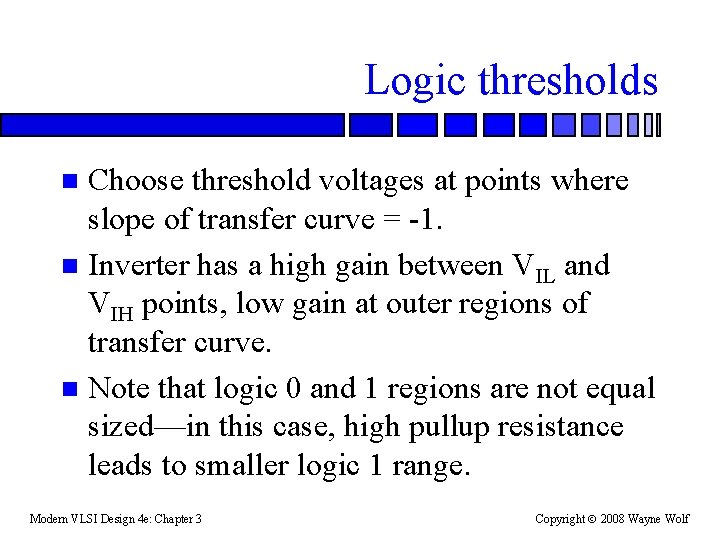
Transfer characteristics n Transfer curve shows static input/output relationship—hold input voltage, measure output voltage. Modern VLSI Design 4 e: Chapter 3 Copyright 2008 Wayne Wolf

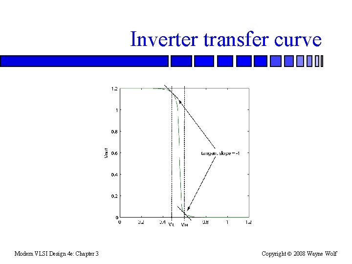
Inverter transfer curve Modern VLSI Design 4 e: Chapter 3 Copyright 2008 Wayne Wolf

Logic thresholds Choose threshold voltages at points where slope of transfer curve = -1. n Inverter has a high gain between VIL and VIH points, low gain at outer regions of transfer curve. n Note that logic 0 and 1 regions are not equal sized—in this case, high pullup resistance leads to smaller logic 1 range. n Modern VLSI Design 4 e: Chapter 3 Copyright 2008 Wayne Wolf

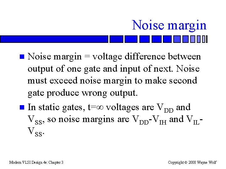
Noise margin = voltage difference between output of one gate and input of next. Noise must exceed noise margin to make second gate produce wrong output. n In static gates, t= voltages are VDD and VSS, so noise margins are VDD-VIH and VILVSS. n Modern VLSI Design 4 e: Chapter 3 Copyright 2008 Wayne Wolf

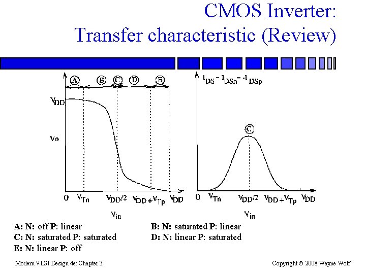
CMOS Inverter: Transfer characteristic (Review) A: N: off P: linear C: N: saturated P: saturated E: N: linear P: off Modern VLSI Design 4 e: Chapter 3 B: N: saturated P: linear D: N: linear P: saturated Copyright 2008 Wayne Wolf

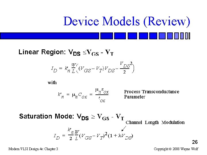
Device Models (Review) 26 Modern VLSI Design 4 e: Chapter 3 Copyright 2008 Wayne Wolf

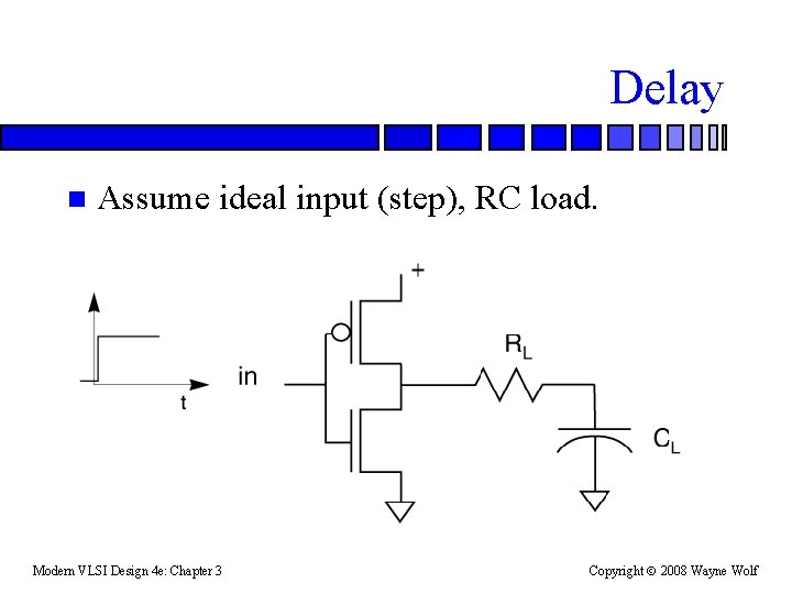
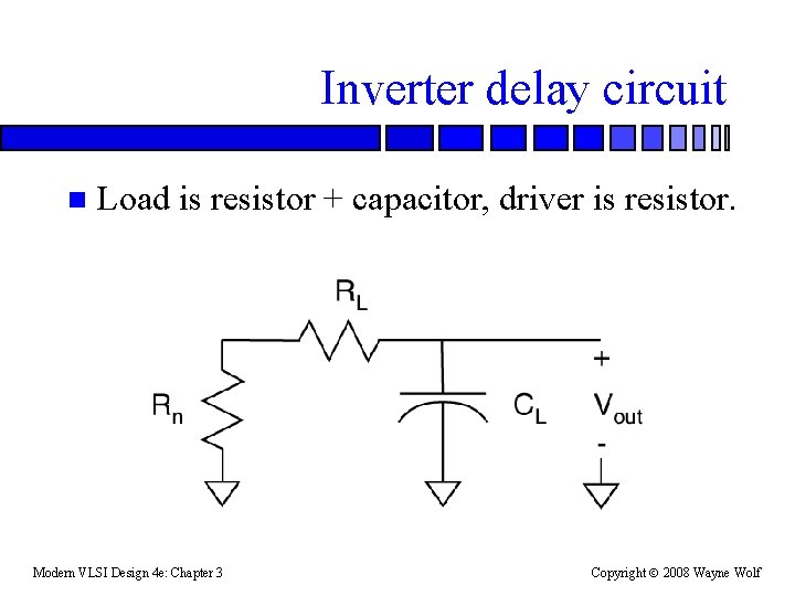
Delay n Assume ideal input (step), RC load. Modern VLSI Design 4 e: Chapter 3 Copyright 2008 Wayne Wolf

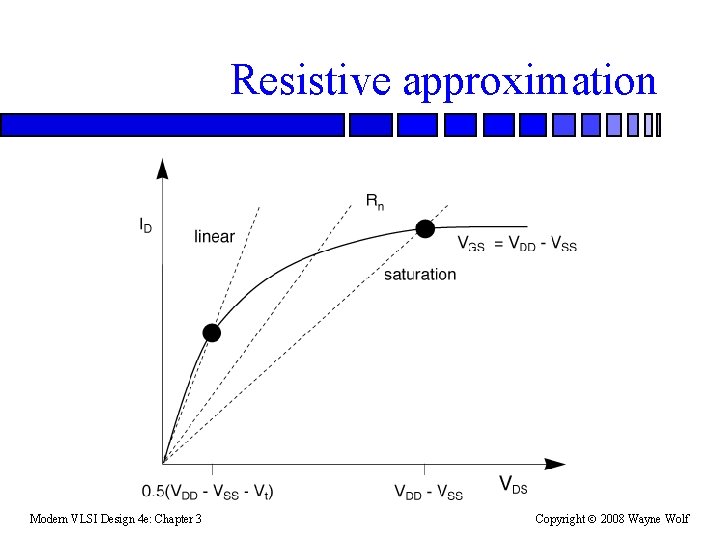
Delay assumptions n Assume that only one transistor is on at a time. This gives two cases: – rise time, pullup on; – fall time, pullup off. n Assume resistor model for transistor. Ignores saturation region and mischaracterizes linear region, but results are acceptable. Modern VLSI Design 4 e: Chapter 3 Copyright 2008 Wayne Wolf

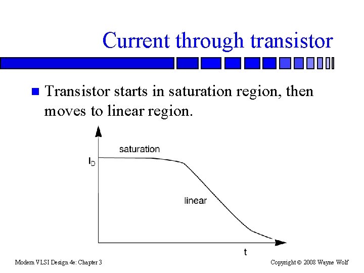
Current through transistor n Transistor starts in saturation region, then moves to linear region. Modern VLSI Design 4 e: Chapter 3 Copyright 2008 Wayne Wolf

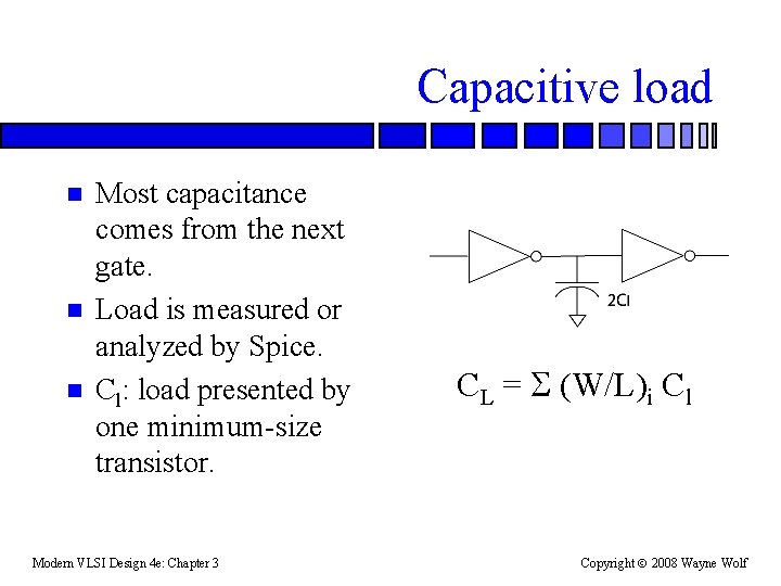
Capacitive load n n n Most capacitance comes from the next gate. Load is measured or analyzed by Spice. Cl: load presented by one minimum-size transistor. Modern VLSI Design 4 e: Chapter 3 CL = S (W/L)i Cl Copyright 2008 Wayne Wolf

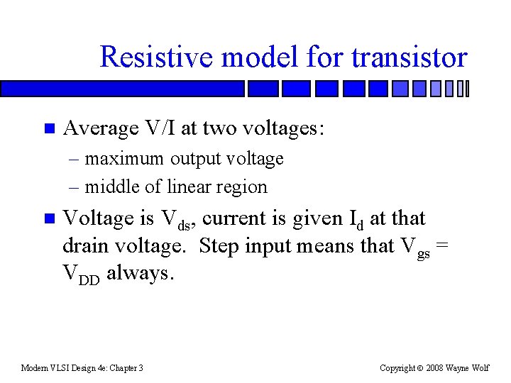
Resistive model for transistor n Average V/I at two voltages: – maximum output voltage – middle of linear region n Voltage is Vds, current is given Id at that drain voltage. Step input means that Vgs = VDD always. Modern VLSI Design 4 e: Chapter 3 Copyright 2008 Wayne Wolf

Resistive approximation Modern VLSI Design 4 e: Chapter 3 Copyright 2008 Wayne Wolf

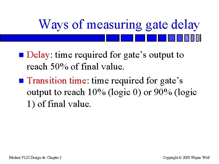
Ways of measuring gate delay Delay: time required for gate’s output to reach 50% of final value. n Transition time: time required for gate’s output to reach 10% (logic 0) or 90% (logic 1) of final value. n Modern VLSI Design 4 e: Chapter 3 Copyright 2008 Wayne Wolf

Inverter delay circuit n Load is resistor + capacitor, driver is resistor. Modern VLSI Design 4 e: Chapter 3 Copyright 2008 Wayne Wolf

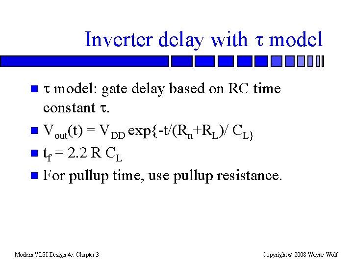
Inverter delay with t model: gate delay based on RC time constant t. n Vout(t) = VDD exp{-t/(Rn+RL)/ CL} n tf = 2. 2 R CL n For pullup time, use pullup resistance. n Modern VLSI Design 4 e: Chapter 3 Copyright 2008 Wayne Wolf

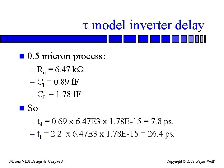
t model inverter delay n 0. 5 micron process: – Rn = 6. 47 k. W – Cl = 0. 89 f. F – CL = 1. 78 f. F n So – td = 0. 69 x 6. 47 E 3 x 1. 78 E-15 = 7. 8 ps. – tf = 2. 2 x 6. 47 E 3 x 1. 78 E-15 = 26. 4 ps. Modern VLSI Design 4 e: Chapter 3 Copyright 2008 Wayne Wolf

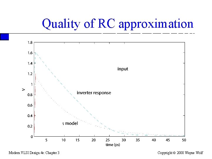
Quality of RC approximation Modern VLSI Design 4 e: Chapter 3 Copyright 2008 Wayne Wolf

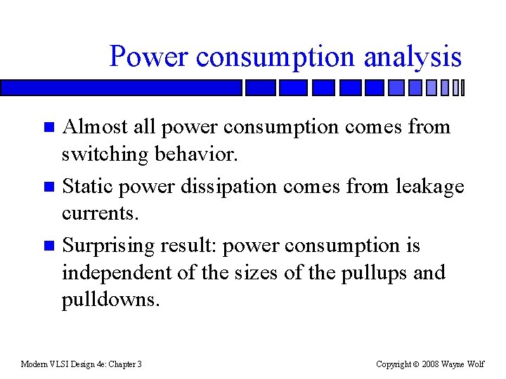
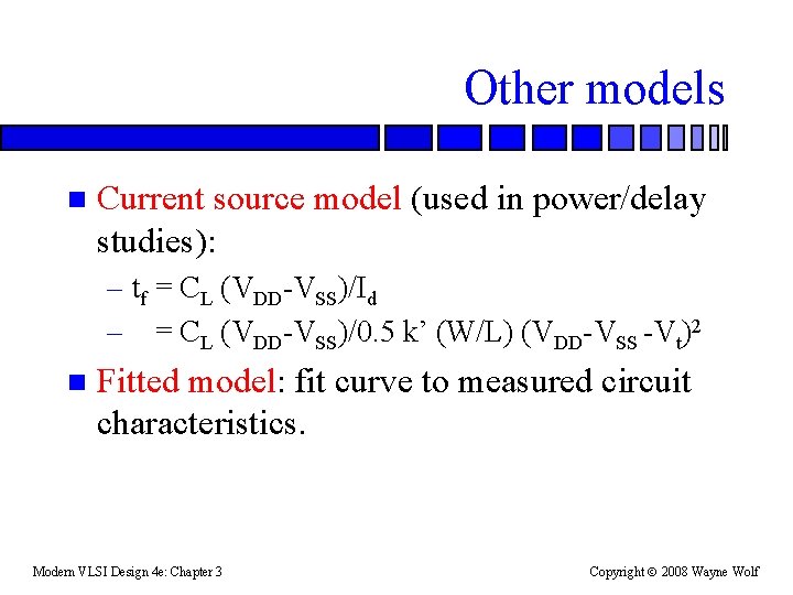
Power consumption analysis Almost all power consumption comes from switching behavior. n Static power dissipation comes from leakage currents. n Surprising result: power consumption is independent of the sizes of the pullups and pulldowns. n Modern VLSI Design 4 e: Chapter 3 Copyright 2008 Wayne Wolf

Other models n Current source model (used in power/delay studies): – tf = CL (VDD-VSS)/Id – = CL (VDD-VSS)/0. 5 k’ (W/L) (VDD-VSS -Vt)2 n Fitted model: fit curve to measured circuit characteristics. Modern VLSI Design 4 e: Chapter 3 Copyright 2008 Wayne Wolf

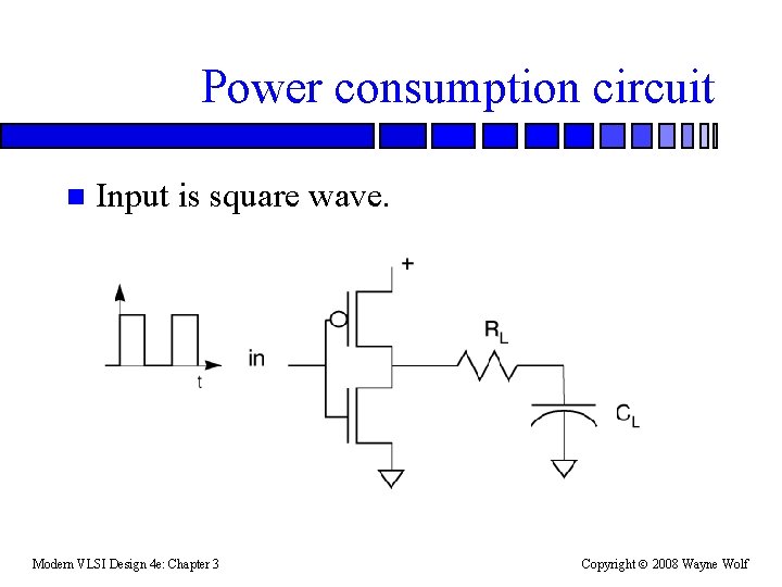
Power consumption circuit n Input is square wave. Modern VLSI Design 4 e: Chapter 3 Copyright 2008 Wayne Wolf

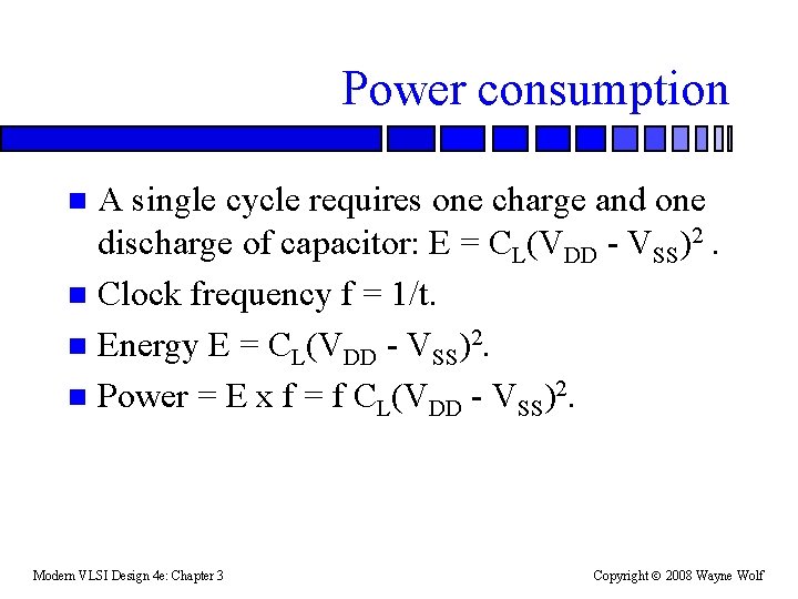
Power consumption A single cycle requires one charge and one discharge of capacitor: E = CL(VDD - VSS)2. n Clock frequency f = 1/t. n Energy E = CL(VDD - VSS)2. n Power = E x f = f CL(VDD - VSS)2. n Modern VLSI Design 4 e: Chapter 3 Copyright 2008 Wayne Wolf

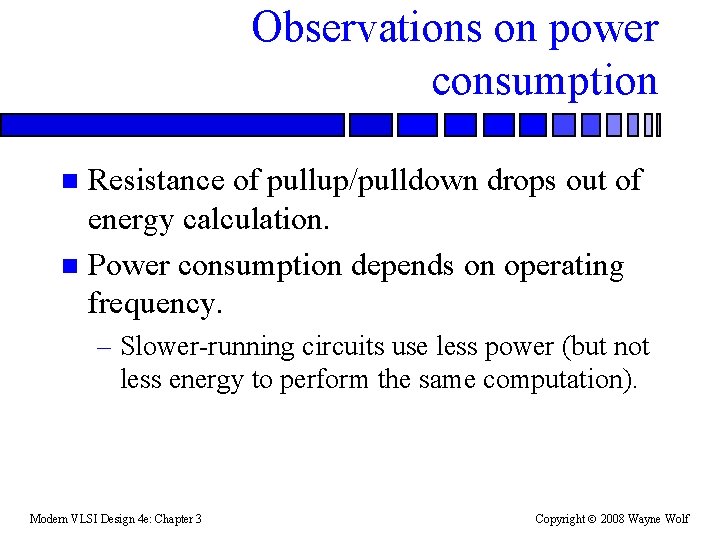
Observations on power consumption Resistance of pullup/pulldown drops out of energy calculation. n Power consumption depends on operating frequency. n – Slower-running circuits use less power (but not less energy to perform the same computation). Modern VLSI Design 4 e: Chapter 3 Copyright 2008 Wayne Wolf

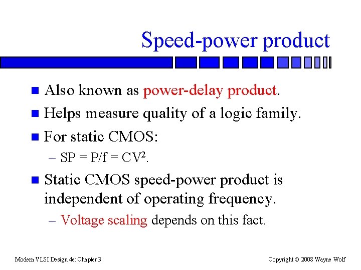
Speed-power product Also known as power-delay product. n Helps measure quality of a logic family. n For static CMOS: n – SP = P/f = CV 2. n Static CMOS speed-power product is independent of operating frequency. – Voltage scaling depends on this fact. Modern VLSI Design 4 e: Chapter 3 Copyright 2008 Wayne Wolf