SingleStage Amplifiers Reference Design of Analog CMOS Integrated
- Slides: 83

Single-Stage Amplifiers Reference: Design of Analog CMOS Integrated Circuits, Behzad Razavi, Mc. Graw-Hill, Second Edition, Chap. 3. Single-Stage Amplifiers 1/83

Overview 1. Why Amplifiers? 5. Common Source Amplifiers 2. Amplifier Characteristics 1. Resistive Load 3. Amplifier Trade-offs 2. Diode-connected Load 4. Single-stage Amplifiers 3. Current Source Load 4. Triode Load 5. Source Degeneration Single-Stage Amplifiers 2/83

Overview 6. Common-Drain (Source-Follower) Amplifiers 1. Resistive Load 2. Current Source Load 3. Voltage Division in Source Followers 7. Common-Gate Amplifiers 6. Cascode Amplifiers Single-Stage Amplifiers 3/83

Why Amplifiers? • Amplifiers are essential building blocks of both analog and digital systems. • Amplifiers are needed for variety of reasons including: – To amplify a weak analog signal for further processing – To reduce the effects of noise of the next stage – To provide a proper logical levels (in digital circuits) • Amplifiers also play a crucial role in feedback systems • We first look at the low-frequency performance of amplifiers. Therefore, all capacitors in the small-signal model are ignored! Single-Stage Amplifiers 4/83

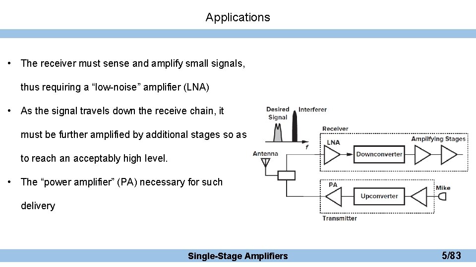
Applications • The receiver must sense and amplify small signals, thus requiring a “low-noise” amplifier (LNA) • As the signal travels down the receive chain, it must be further amplified by additional stages so as to reach an acceptably high level. • The “power amplifier” (PA) necessary for such delivery Single-Stage Amplifiers 5/83

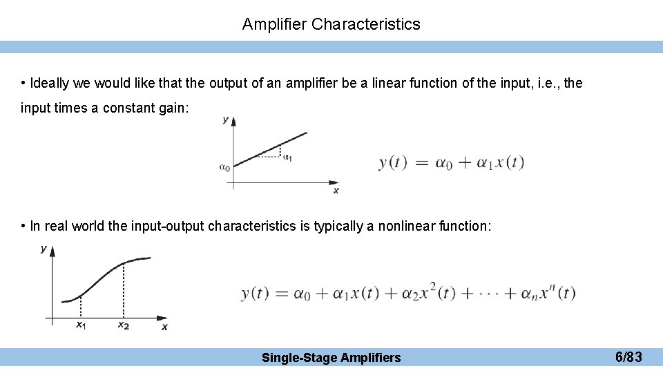
Amplifier Characteristics • Ideally we would like that the output of an amplifier be a linear function of the input, i. e. , the input times a constant gain: • In real world the input-output characteristics is typically a nonlinear function: Single-Stage Amplifiers 6/83

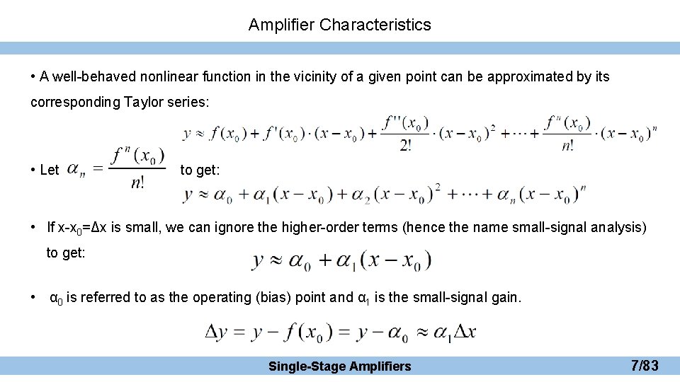
Amplifier Characteristics • A well-behaved nonlinear function in the vicinity of a given point can be approximated by its corresponding Taylor series: • Let to get: • If x-x 0=Δx is small, we can ignore the higher-order terms (hence the name small-signal analysis) to get: • α 0 is referred to as the operating (bias) point and α 1 is the small-signal gain. Single-Stage Amplifiers 7/83

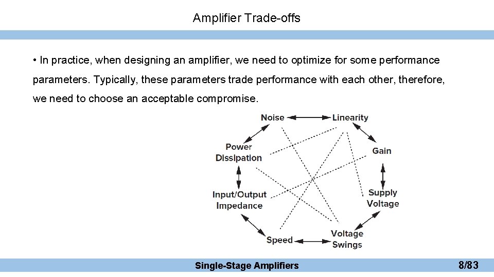
Amplifier Trade-offs • In practice, when designing an amplifier, we need to optimize for some performance parameters. Typically, these parameters trade performance with each other, therefore, we need to choose an acceptable compromise. Single-Stage Amplifiers 8/83

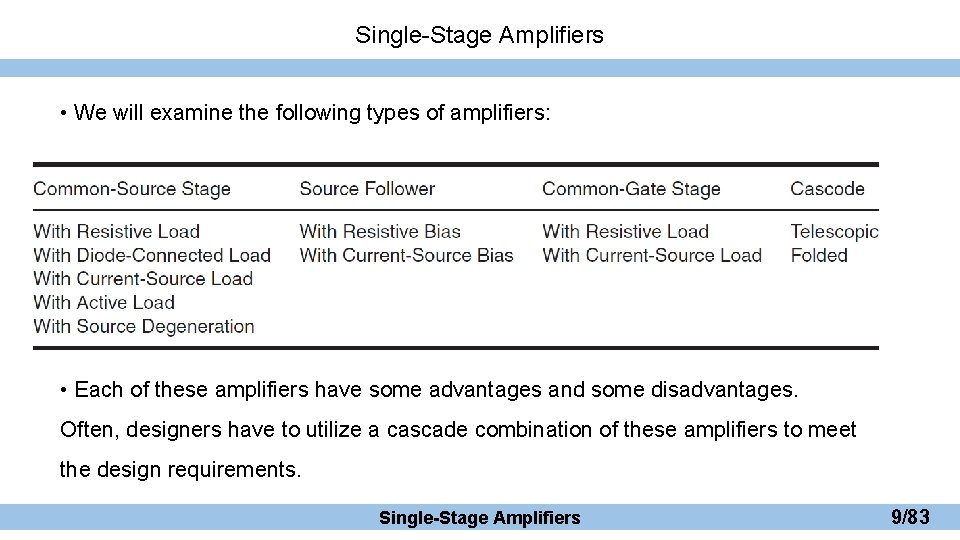
Single-Stage Amplifiers • We will examine the following types of amplifiers: • Each of these amplifiers have some advantages and some disadvantages. Often, designers have to utilize a cascade combination of these amplifiers to meet the design requirements. Single-Stage Amplifiers 9/83

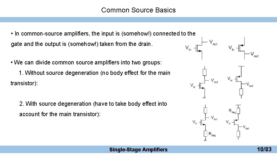
Common Source Basics • In common-source amplifiers, the input is (somehow!) connected to the gate and the output is (somehow!) taken from the drain. • We can divide common source amplifiers into two groups: 1. Without source degeneration (no body effect for the main transistor): 2. With source degeneration (have to take body effect into account for the main transistor): Single-Stage Amplifiers 10/83

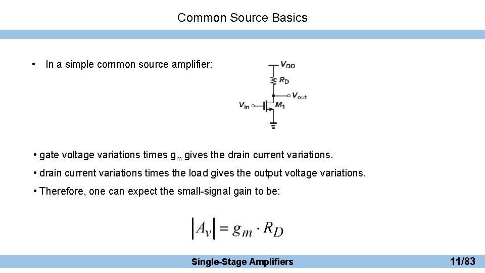
Common Source Basics • In a simple common source amplifier: • gate voltage variations times gm gives the drain current variations. • drain current variations times the load gives the output voltage variations. • Therefore, one can expect the small-signal gain to be: Single-Stage Amplifiers 11/83

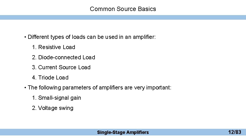
Common Source Basics • Different types of loads can be used in an amplifier: 1. Resistive Load 2. Diode-connected Load 3. Current Source Load 4. Triode Load • The following parameters of amplifiers are very important: 1. Small-signal gain 2. Voltage swing Single-Stage Amplifiers 12/83

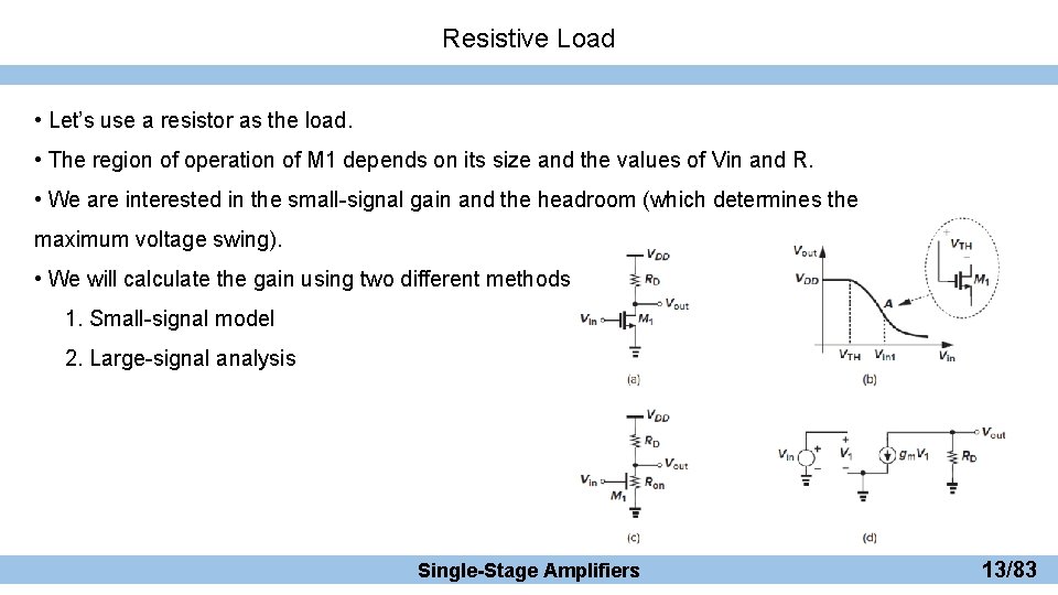
Resistive Load • Let’s use a resistor as the load. • The region of operation of M 1 depends on its size and the values of Vin and R. • We are interested in the small-signal gain and the headroom (which determines the maximum voltage swing). • We will calculate the gain using two different methods 1. Small-signal model 2. Large-signal analysis Single-Stage Amplifiers 13/83

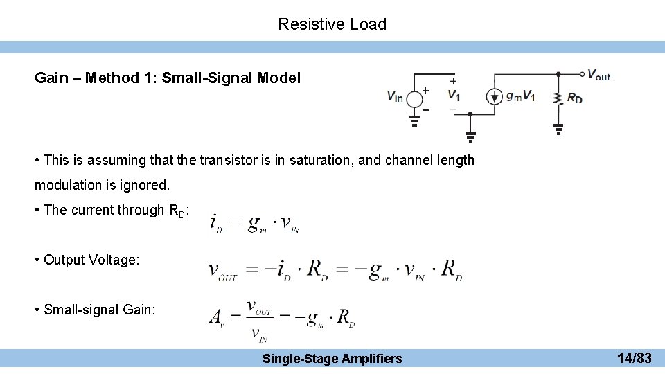
Resistive Load Gain – Method 1: Small-Signal Model • This is assuming that the transistor is in saturation, and channel length modulation is ignored. • The current through RD: • Output Voltage: • Small-signal Gain: Single-Stage Amplifiers 14/83

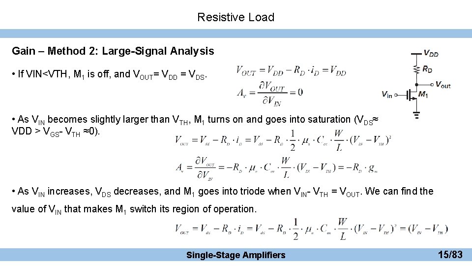
Resistive Load Gain – Method 2: Large-Signal Analysis • If VIN<VTH, M 1 is off, and VOUT= VDD = VDS. • As VIN becomes slightly larger than VTH, M 1 turns on and goes into saturation (VDS≈ VDD > VGS- VTH ≈0). • As VIN increases, VDS decreases, and M 1 goes into triode when VIN- VTH = VOUT. We can find the value of VIN that makes M 1 switch its region of operation. Single-Stage Amplifiers 15/83

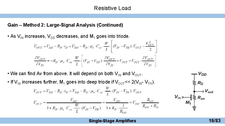
Resistive Load Gain – Method 2: Large-Signal Analysis (Continued) • As VIN increases, VDS decreases, and M 1 goes into triode. • We can find Av from above. It will depend on both VIN and VOUT. • If VIN increases further, M 1 goes into deep triode if VOUT<< 2(VIN- VTH). Single-Stage Amplifiers 16/83

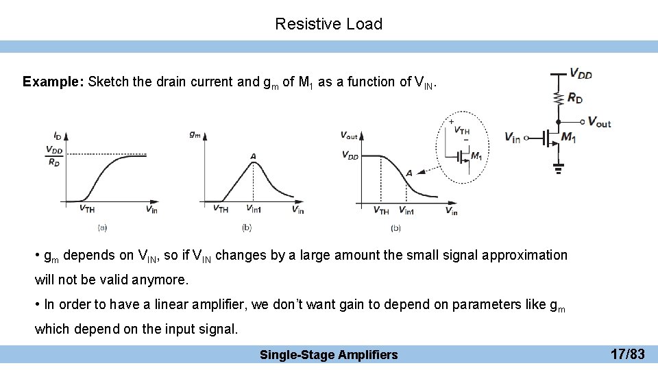
Resistive Load Example: Sketch the drain current and gm of M 1 as a function of VIN. • gm depends on VIN, so if VIN changes by a large amount the small signal approximation will not be valid anymore. • In order to have a linear amplifier, we don’t want gain to depend on parameters like gm which depend on the input signal. Single-Stage Amplifiers 17/83

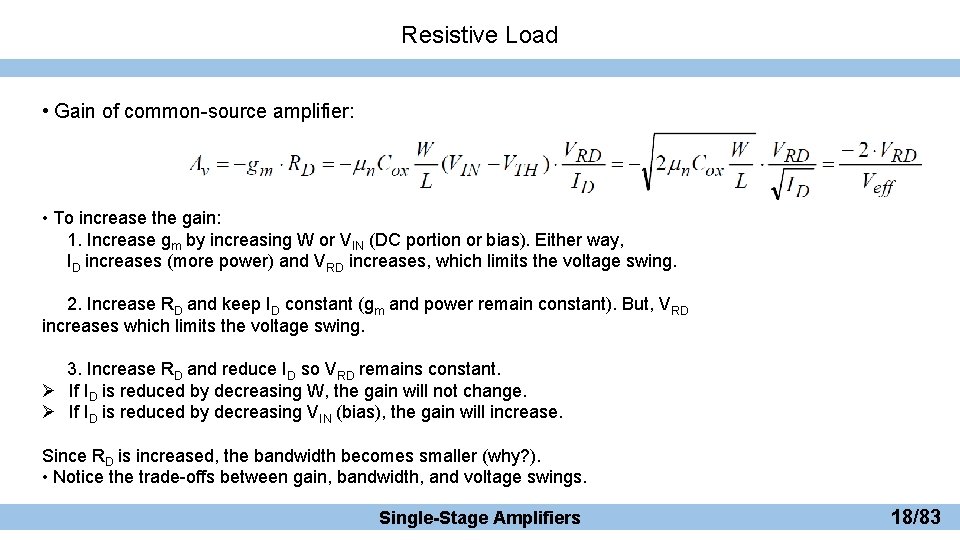
Resistive Load • Gain of common-source amplifier: • To increase the gain: 1. Increase gm by increasing W or VIN (DC portion or bias). Either way, ID increases (more power) and VRD increases, which limits the voltage swing. 2. Increase RD and keep ID constant (gm and power remain constant). But, VRD increases which limits the voltage swing. 3. Increase RD and reduce ID so VRD remains constant. Ø If ID is reduced by decreasing W, the gain will not change. Ø If ID is reduced by decreasing VIN (bias), the gain will increase. Since RD is increased, the bandwidth becomes smaller (why? ). • Notice the trade-offs between gain, bandwidth, and voltage swings. Single-Stage Amplifiers 18/83

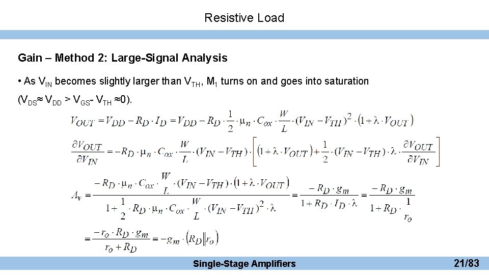
Resistive Load • Now let’s consider the simple common-source circuit with channel length modulation taken into account. • Channel length modulation becomes more important as RD increases (in the next slide we will see why!). • Again, we will calculate the gain in two different methods 1. Small-signal Model 2. Large Signal Analysis Single-Stage Amplifiers 19/83

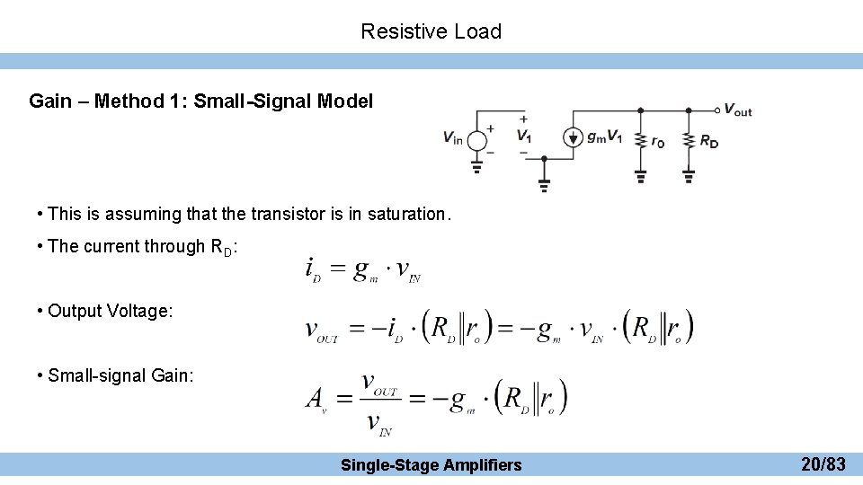
Resistive Load Gain – Method 1: Small-Signal Model • This is assuming that the transistor is in saturation. • The current through RD: • Output Voltage: • Small-signal Gain: Single-Stage Amplifiers 20/83

Resistive Load Gain – Method 2: Large-Signal Analysis • As VIN becomes slightly larger than VTH, M 1 turns on and goes into saturation (VDS≈ VDD > VGS- VTH ≈0). Single-Stage Amplifiers 21/83

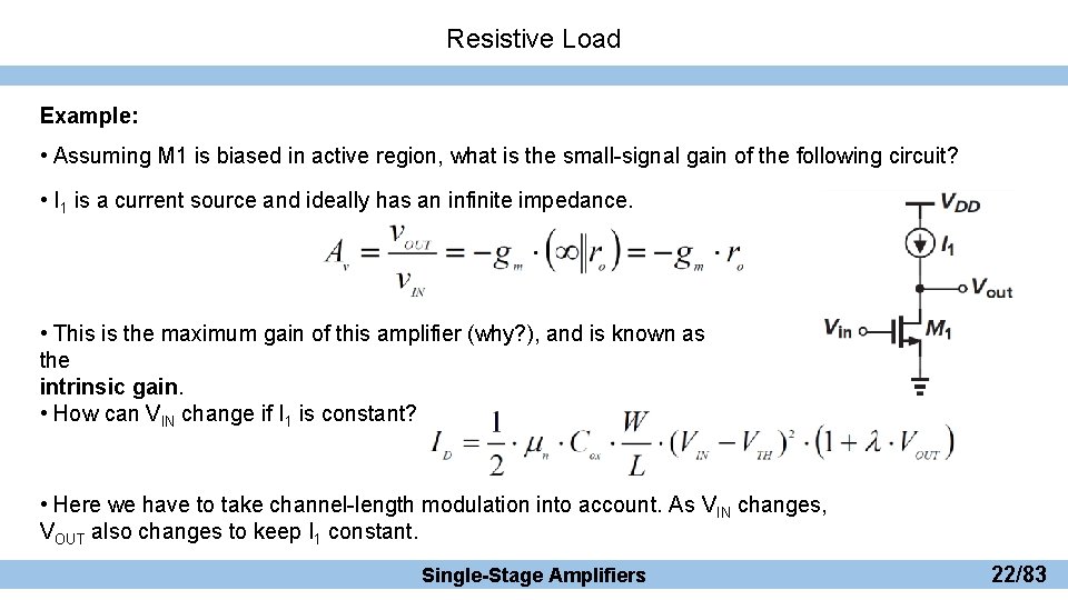
Resistive Load Example: • Assuming M 1 is biased in active region, what is the small-signal gain of the following circuit? • I 1 is a current source and ideally has an infinite impedance. • This is the maximum gain of this amplifier (why? ), and is known as the intrinsic gain. • How can VIN change if I 1 is constant? • Here we have to take channel-length modulation into account. As VIN changes, VOUT also changes to keep I 1 constant. Single-Stage Amplifiers 22/83

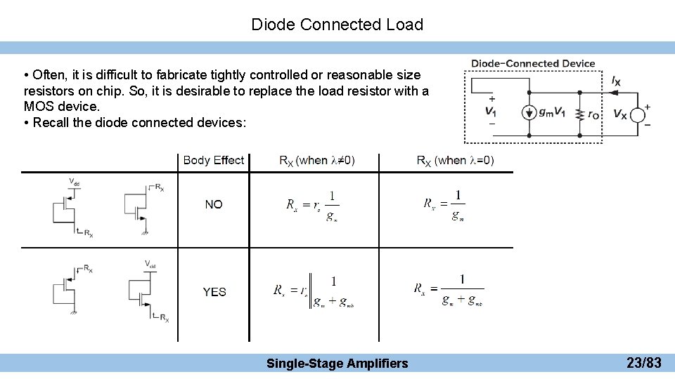
Diode Connected Load • Often, it is difficult to fabricate tightly controlled or reasonable size resistors on chip. So, it is desirable to replace the load resistor with a MOS device. • Recall the diode connected devices: Single-Stage Amplifiers 23/83

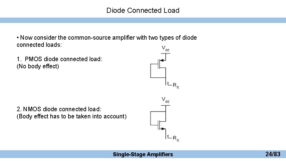
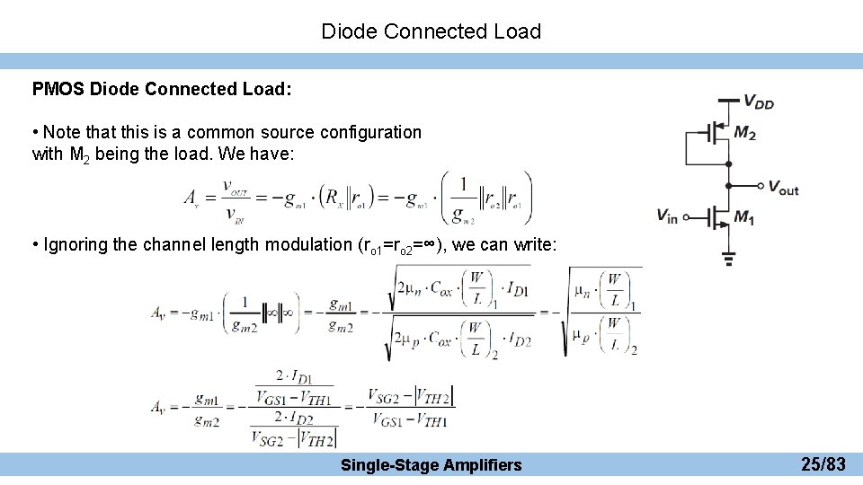
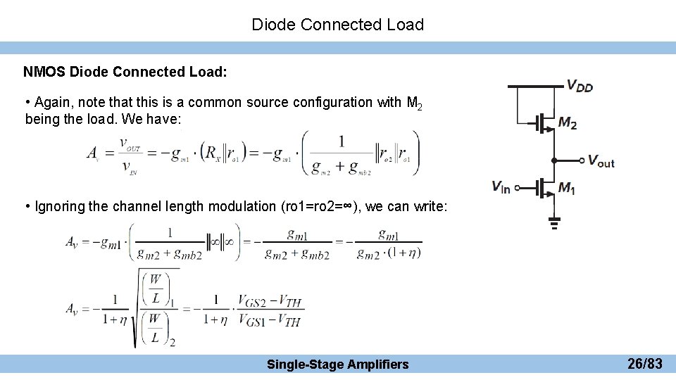
Diode Connected Load • Now consider the common-source amplifier with two types of diode connected loads: 1. PMOS diode connected load: (No body effect) 2. NMOS diode connected load: (Body effect has to be taken into account) Single-Stage Amplifiers 24/83

Diode Connected Load PMOS Diode Connected Load: • Note that this is a common source configuration with M 2 being the load. We have: • Ignoring the channel length modulation (ro 1=ro 2=∞), we can write: Single-Stage Amplifiers 25/83

Diode Connected Load NMOS Diode Connected Load: • Again, note that this is a common source configuration with M 2 being the load. We have: • Ignoring the channel length modulation (ro 1=ro 2=∞), we can write: Single-Stage Amplifiers 26/83

Diode Connected Load • For a diode connected load we observe that (to the first order approximation): 1. The amplifier gain is not a function of the bias current. So, the change in the input and output levels does not affect the gain, and the amplifier becomes more linear. 2. The amplifier gain is not a function of the input signal (amplifier becomes more linear). 3. The amplifier gain is a weak function (square root) of the transistor sizes. So, we have to change the dimensions by a considerable amount so as to increase the gain. Single-Stage Amplifiers 27/83

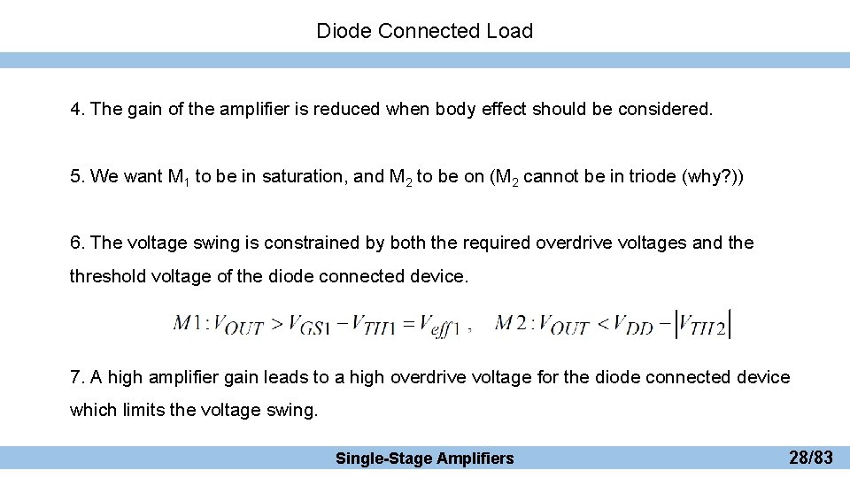
Diode Connected Load 4. The gain of the amplifier is reduced when body effect should be considered. 5. We want M 1 to be in saturation, and M 2 to be on (M 2 cannot be in triode (why? )) 6. The voltage swing is constrained by both the required overdrive voltages and the threshold voltage of the diode connected device. 7. A high amplifier gain leads to a high overdrive voltage for the diode connected device which limits the voltage swing. Single-Stage Amplifiers 28/83

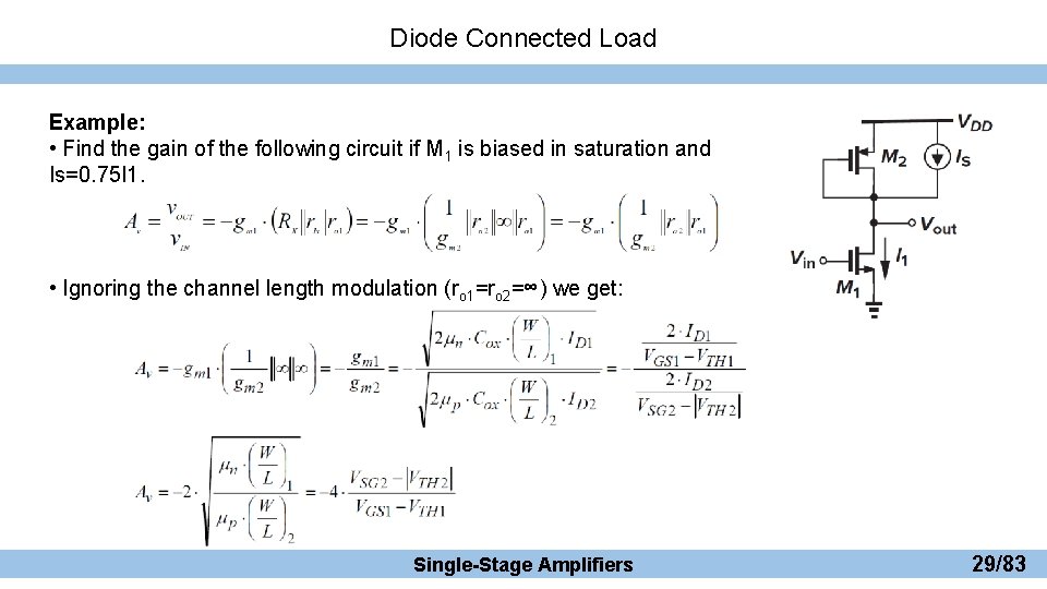
Diode Connected Load Example: • Find the gain of the following circuit if M 1 is biased in saturation and Is=0. 75 I 1. • Ignoring the channel length modulation (ro 1=ro 2=∞) we get: Single-Stage Amplifiers 29/83

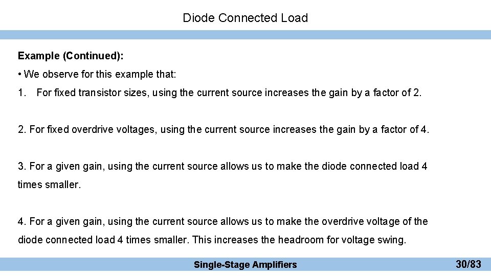
Diode Connected Load Example (Continued): • We observe for this example that: 1. For fixed transistor sizes, using the current source increases the gain by a factor of 2. 2. For fixed overdrive voltages, using the current source increases the gain by a factor of 4. 3. For a given gain, using the current source allows us to make the diode connected load 4 times smaller. 4. For a given gain, using the current source allows us to make the overdrive voltage of the diode connected load 4 times smaller. This increases the headroom for voltage swing. Single-Stage Amplifiers 30/83

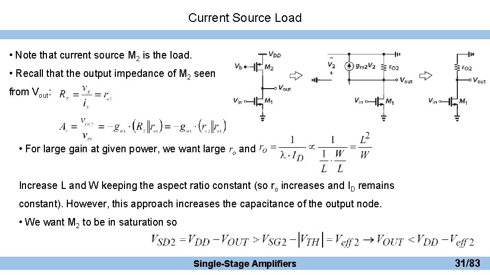
Current Source Load • Note that current source M 2 is the load. • Recall that the output impedance of M 2 seen from Vout: • For large gain at given power, we want large ro and Increase L and W keeping the aspect ratio constant (so ro increases and ID remains constant). However, this approach increases the capacitance of the output node. • We want M 2 to be in saturation so Single-Stage Amplifiers 31/83

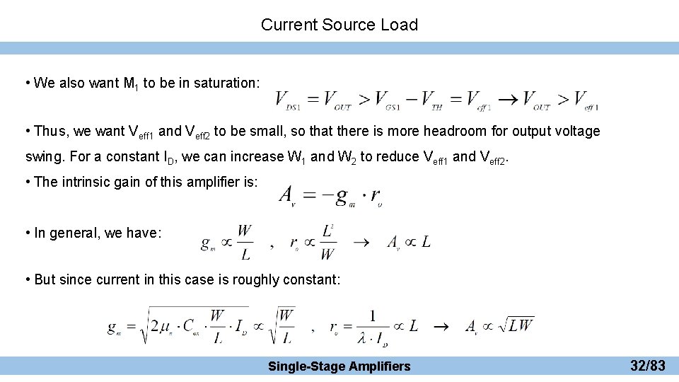
Current Source Load • We also want M 1 to be in saturation: • Thus, we want Veff 1 and Veff 2 to be small, so that there is more headroom for output voltage swing. For a constant ID, we can increase W 1 and W 2 to reduce Veff 1 and Veff 2. • The intrinsic gain of this amplifier is: • In general, we have: • But since current in this case is roughly constant: Single-Stage Amplifiers 32/83

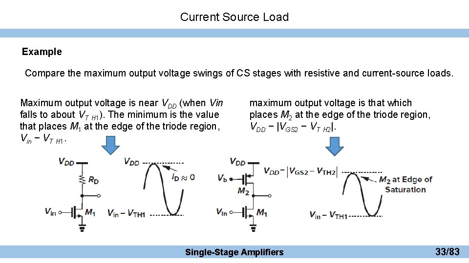
Current Source Load Example Compare the maximum output voltage swings of CS stages with resistive and current-source loads. Maximum output voltage is near VDD (when Vin falls to about VT H 1). The minimum is the value that places M 1 at the edge of the triode region, Vin − VT H 1. maximum output voltage is that which places M 2 at the edge of the triode region, VDD − |VGS 2 − VT H 2|. Single-Stage Amplifiers 33/83

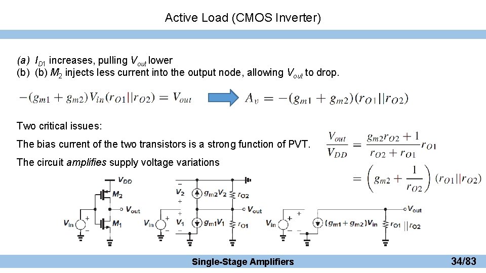
Active Load (CMOS Inverter) (a) ID 1 increases, pulling Vout lower (b) M 2 injects less current into the output node, allowing Vout to drop. Two critical issues: The bias current of the two transistors is a strong function of PVT. The circuit amplifies supply voltage variations Single-Stage Amplifiers 34/83

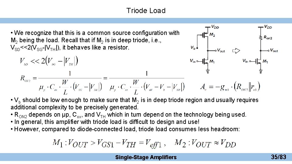
Triode Load • We recognize that this is a common source configuration with M 2 being the load. Recall that if M 2 is in deep triode, i. e. , VSD<<2(VSG-|VTH|), it behaves like a resistor. • Vb should be low enough to make sure that M 2 is in deep triode region and usually requires additional complexity to be precisely generated. • RON 2 depends on μp, Cox, and VTH which in turn depend on the technology being used. • In general, this amplifier with triode load is difficult to design and use! • However, compared to diode-connected load, triode load consumes less headroom: Single-Stage Amplifiers 35/83

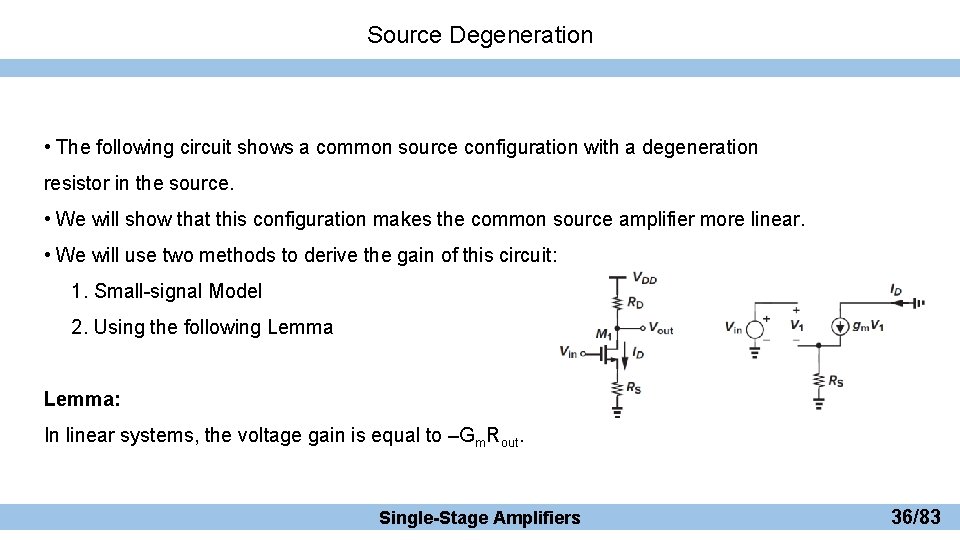
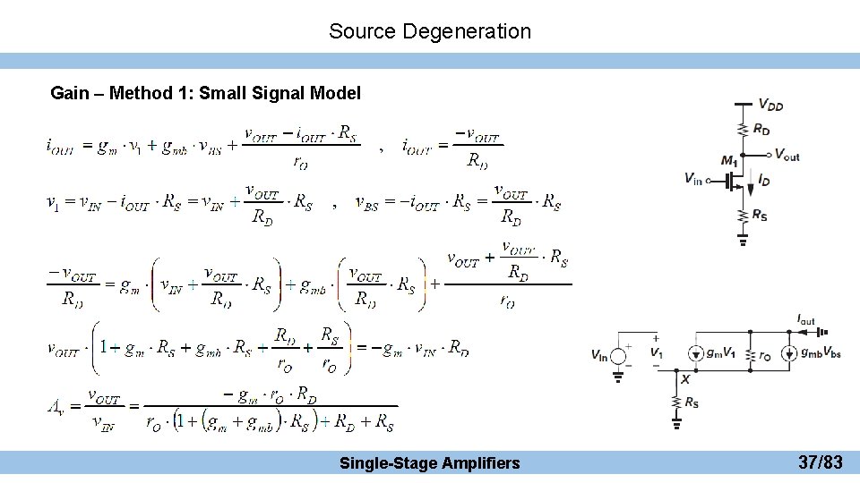
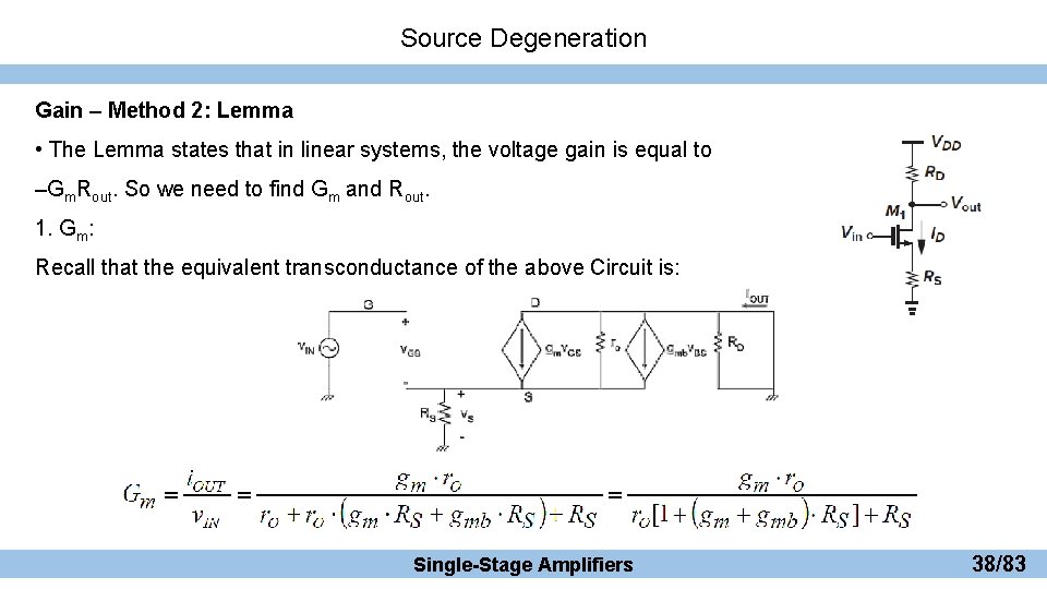
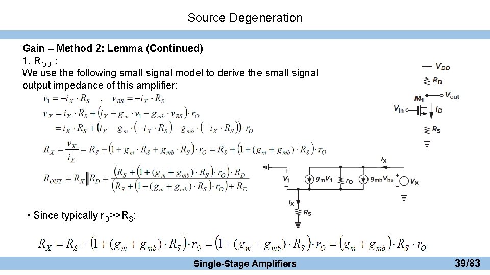
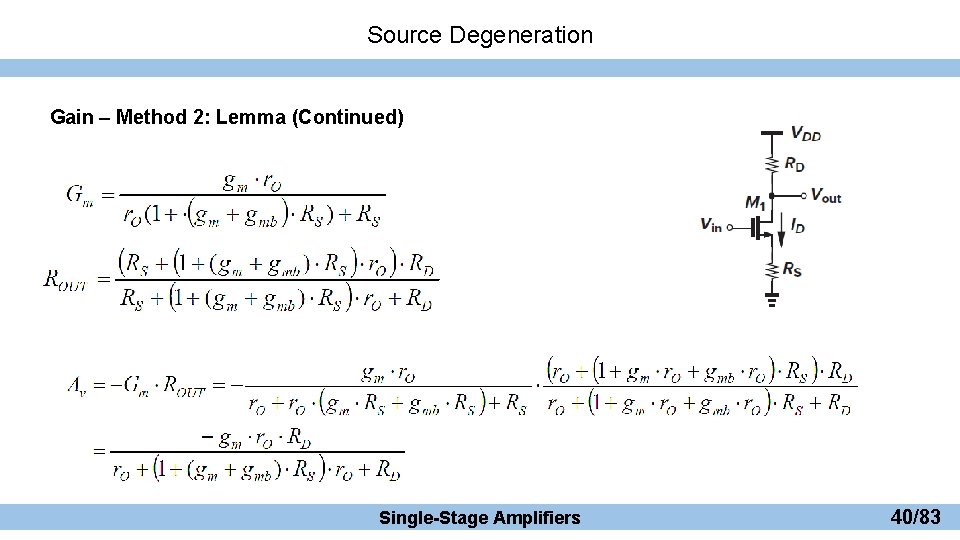
Source Degeneration • The following circuit shows a common source configuration with a degeneration resistor in the source. • We will show that this configuration makes the common source amplifier more linear. • We will use two methods to derive the gain of this circuit: 1. Small-signal Model 2. Using the following Lemma: In linear systems, the voltage gain is equal to –Gm. Rout. Single-Stage Amplifiers 36/83

Source Degeneration Gain – Method 1: Small Signal Model Single-Stage Amplifiers 37/83

Source Degeneration Gain – Method 2: Lemma • The Lemma states that in linear systems, the voltage gain is equal to –Gm. Rout. So we need to find Gm and Rout. 1. Gm: Recall that the equivalent transconductance of the above Circuit is: Single-Stage Amplifiers 38/83

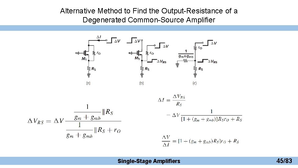
Source Degeneration Gain – Method 2: Lemma (Continued) 1. ROUT: We use the following small signal model to derive the small signal output impedance of this amplifier: • Since typically r. O>>RS: Single-Stage Amplifiers 39/83

Source Degeneration Gain – Method 2: Lemma (Continued) Single-Stage Amplifiers 40/83

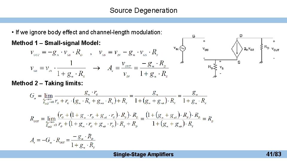
Source Degeneration • If we ignore body effect and channel-length modulation: Method 1 – Small-signal Model: Method 2 – Taking limits: Single-Stage Amplifiers 41/83

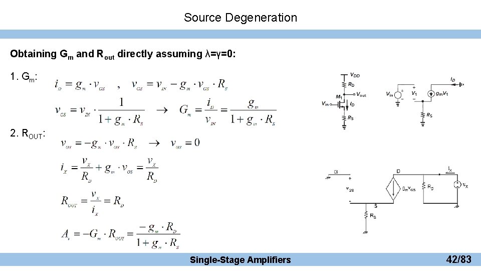
Source Degeneration Obtaining Gm and Rout directly assuming λ=γ=0: 1. Gm: 2. ROUT: Single-Stage Amplifiers 42/83

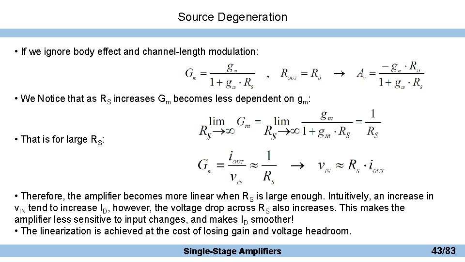
Source Degeneration • If we ignore body effect and channel-length modulation: • We Notice that as RS increases Gm becomes less dependent on gm: • That is for large RS: • Therefore, the amplifier becomes more linear when RS is large enough. Intuitively, an increase in v. IN tend to increase ID, however, the voltage drop across RS also increases. This makes the amplifier less sensitive to input changes, and makes ID smoother! • The linearization is achieved at the cost of losing gain and voltage headroom. Single-Stage Amplifiers 43/83

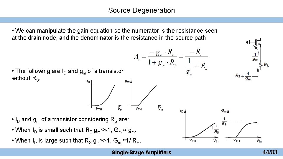
Source Degeneration • We can manipulate the gain equation so the numerator is the resistance seen at the drain node, and the denominator is the resistance in the source path. • The following are ID and gm of a transistor without RS. • ID and gm of a transistor considering RS are: • When ID is small such that RS gm<<1, Gm ≈ gm. • When ID is large such that RS gm>>1, Gm ≈1/ RS. Single-Stage Amplifiers 44/83

Alternative Method to Find the Output-Resistance of a Degenerated Common-Source Amplifier Single-Stage Amplifiers 45/83

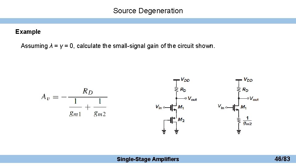
Source Degeneration Example Assuming λ = γ = 0, calculate the small-signal gain of the circuit shown. Single-Stage Amplifiers 46/83

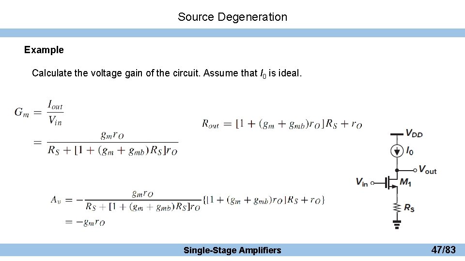
Source Degeneration Example Calculate the voltage gain of the circuit. Assume that I 0 is ideal. Single-Stage Amplifiers 47/83

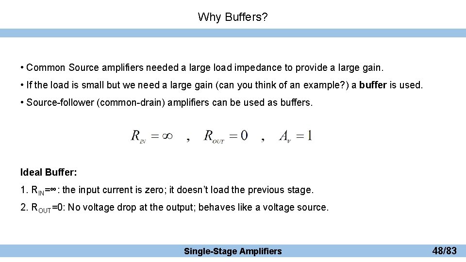
Why Buffers? • Common Source amplifiers needed a large load impedance to provide a large gain. • If the load is small but we need a large gain (can you think of an example? ) a buffer is used. • Source-follower (common-drain) amplifiers can be used as buffers. Ideal Buffer: 1. RIN=∞: the input current is zero; it doesn’t load the previous stage. 2. ROUT=0: No voltage drop at the output; behaves like a voltage source. Single-Stage Amplifiers 48/83

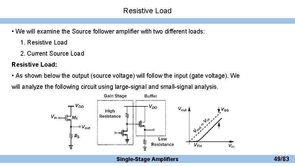
Resistive Load • We will examine the Source follower amplifier with two different loads: 1. Resistive Load 2. Current Source Load Resistive Load: • As shown below the output (source voltage) will follow the input (gate voltage). We will analyze the following circuit using large-signal and small-signal analysis. Single-Stage Amplifiers 49/83

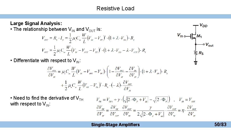
Resistive Load Large Signal Analysis: • The relationship between VIN and VOUT is: • Differentiate with respect to VIN: • Need to find the derivative of VTH with respect to VIN: Single-Stage Amplifiers 50/83

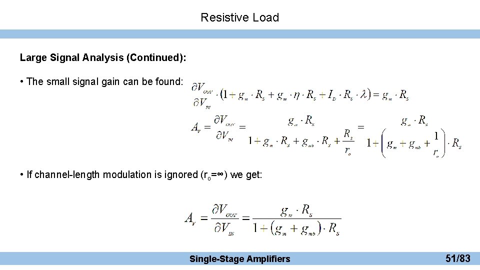
Resistive Load Large Signal Analysis (Continued): • The small signal gain can be found: • If channel-length modulation is ignored (ro=∞) we get: Single-Stage Amplifiers 51/83

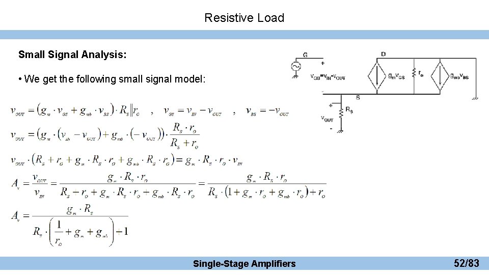
Resistive Load Small Signal Analysis: • We get the following small signal model: Single-Stage Amplifiers 52/83

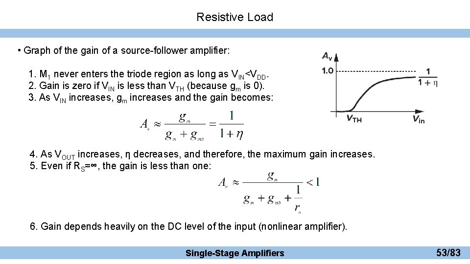
Resistive Load • Graph of the gain of a source-follower amplifier: 1. M 1 never enters the triode region as long as VIN<VDD. 2. Gain is zero if VIN is less than VTH (because gm is 0). 3. As VIN increases, gm increases and the gain becomes: 4. As VOUT increases, η decreases, and therefore, the maximum gain increases. 5. Even if RS=∞, the gain is less than one: 6. Gain depends heavily on the DC level of the input (nonlinear amplifier). Single-Stage Amplifiers 53/83

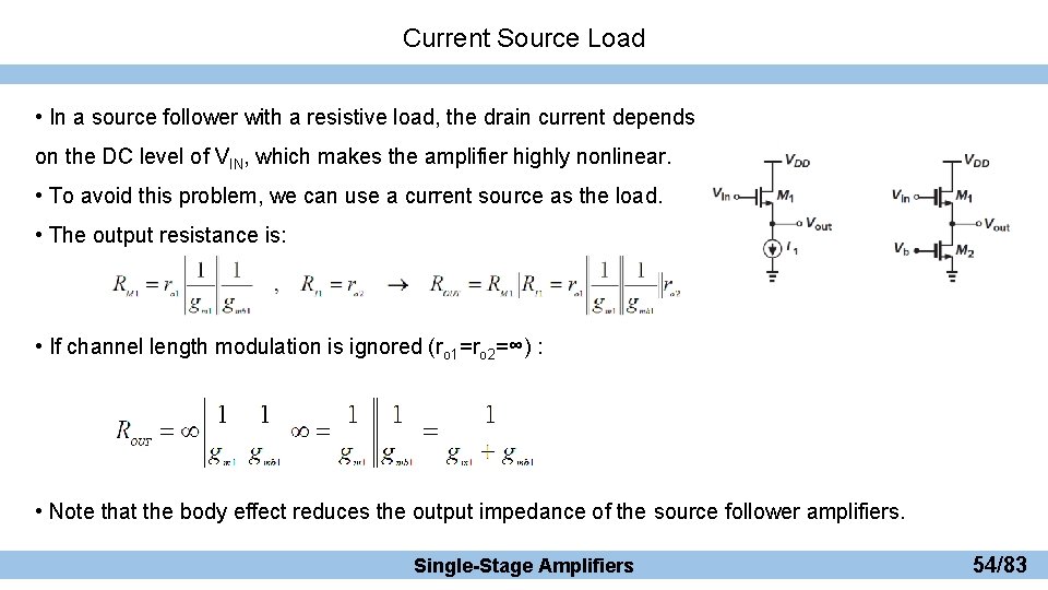
Current Source Load • In a source follower with a resistive load, the drain current depends on the DC level of VIN, which makes the amplifier highly nonlinear. • To avoid this problem, we can use a current source as the load. • The output resistance is: • If channel length modulation is ignored (ro 1=ro 2=∞) : • Note that the body effect reduces the output impedance of the source follower amplifiers. Single-Stage Amplifiers 54/83

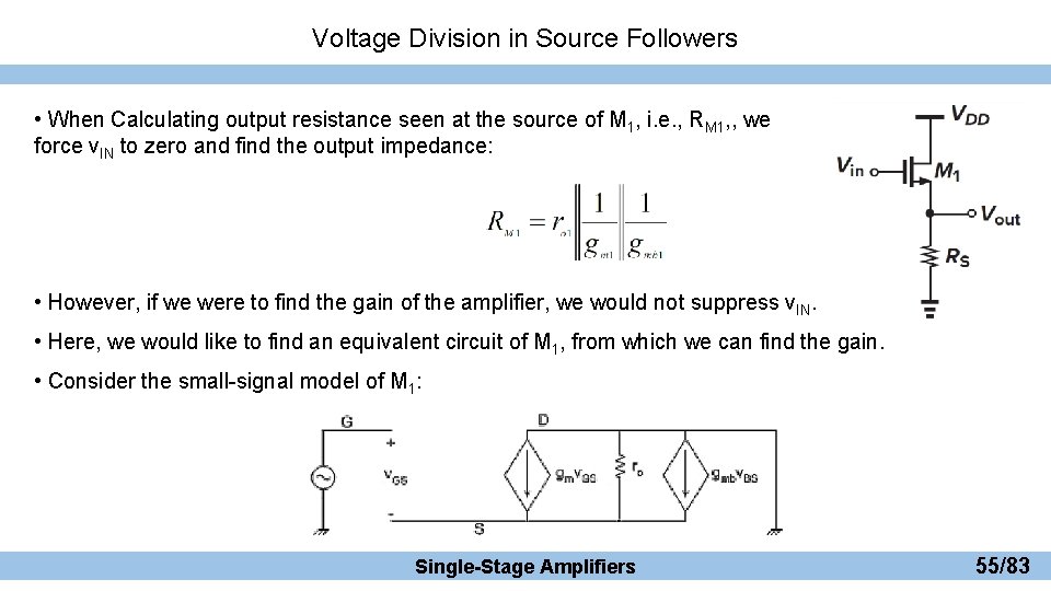
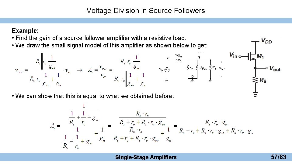
Voltage Division in Source Followers • When Calculating output resistance seen at the source of M 1, i. e. , RM 1, , we force v. IN to zero and find the output impedance: • However, if we were to find the gain of the amplifier, we would not suppress v. IN. • Here, we would like to find an equivalent circuit of M 1, from which we can find the gain. • Consider the small-signal model of M 1: Single-Stage Amplifiers 55/83

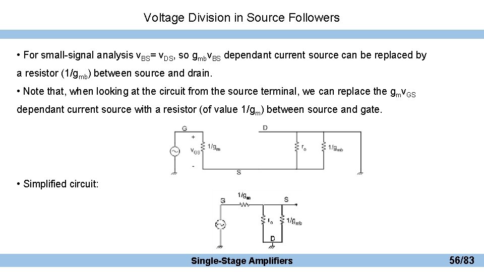
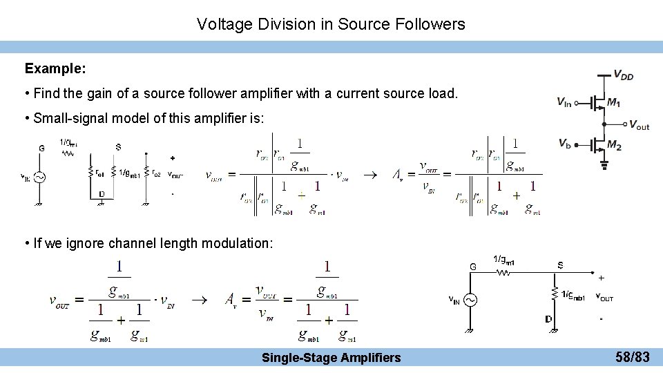
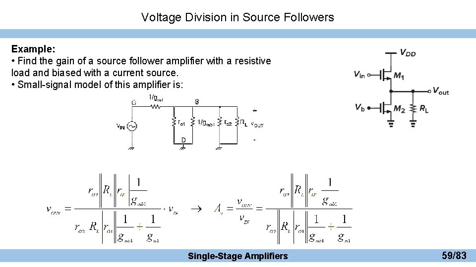
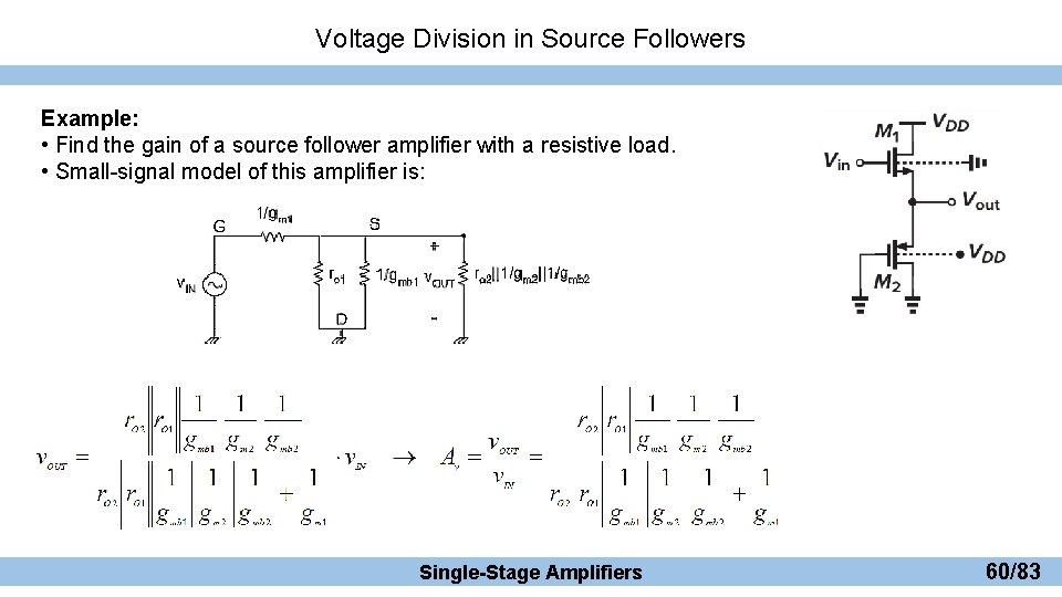
Voltage Division in Source Followers • For small-signal analysis v. BS= v. DS, so gmbv. BS dependant current source can be replaced by a resistor (1/gmb) between source and drain. • Note that, when looking at the circuit from the source terminal, we can replace the gmv. GS dependant current source with a resistor (of value 1/gm) between source and gate. • Simplified circuit: Single-Stage Amplifiers 56/83

Voltage Division in Source Followers Example: • Find the gain of a source follower amplifier with a resistive load. • We draw the small signal model of this amplifier as shown below to get: • We can show that this is equal to what we obtained before: Single-Stage Amplifiers 57/83

Voltage Division in Source Followers Example: • Find the gain of a source follower amplifier with a current source load. • Small-signal model of this amplifier is: • If we ignore channel length modulation: Single-Stage Amplifiers 58/83

Voltage Division in Source Followers Example: • Find the gain of a source follower amplifier with a resistive load and biased with a current source. • Small-signal model of this amplifier is: Single-Stage Amplifiers 59/83

Voltage Division in Source Followers Example: • Find the gain of a source follower amplifier with a resistive load. • Small-signal model of this amplifier is: Single-Stage Amplifiers 60/83

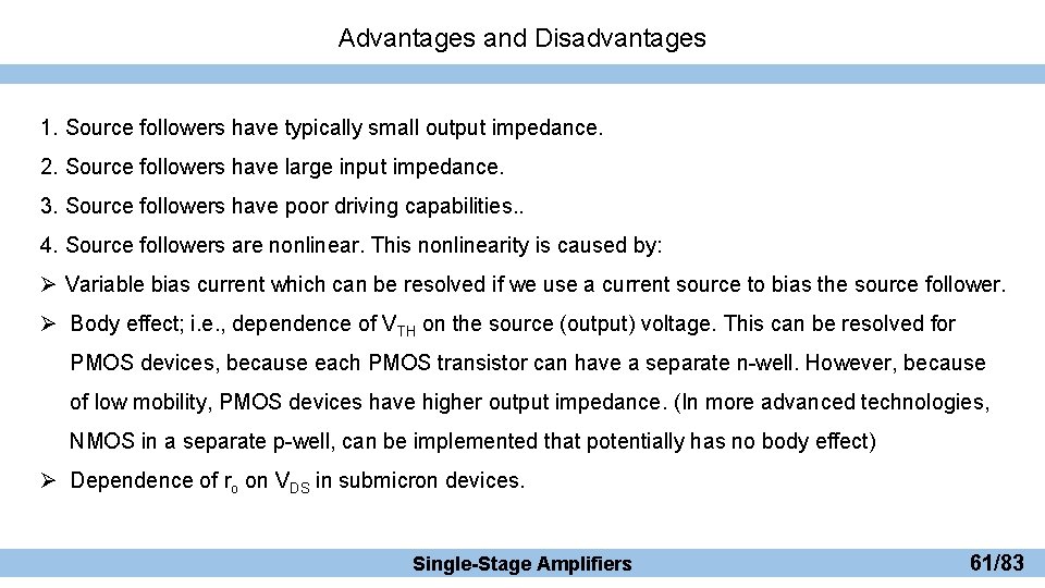
Advantages and Disadvantages 1. Source followers have typically small output impedance. 2. Source followers have large input impedance. 3. Source followers have poor driving capabilities. . 4. Source followers are nonlinear. This nonlinearity is caused by: Ø Variable bias current which can be resolved if we use a current source to bias the source follower. Ø Body effect; i. e. , dependence of VTH on the source (output) voltage. This can be resolved for PMOS devices, because each PMOS transistor can have a separate n-well. However, because of low mobility, PMOS devices have higher output impedance. (In more advanced technologies, NMOS in a separate p-well, can be implemented that potentially has no body effect) Ø Dependence of ro on VDS in submicron devices. Single-Stage Amplifiers 61/83

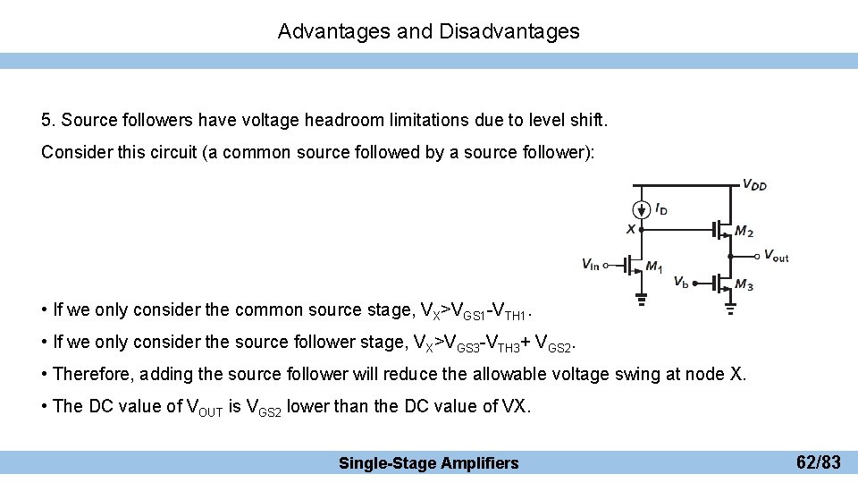
Advantages and Disadvantages 5. Source followers have voltage headroom limitations due to level shift. Consider this circuit (a common source followed by a source follower): • If we only consider the common source stage, VX>VGS 1 -VTH 1. • If we only consider the source follower stage, VX>VGS 3 -VTH 3+ VGS 2. • Therefore, adding the source follower will reduce the allowable voltage swing at node X. • The DC value of VOUT is VGS 2 lower than the DC value of VX. Single-Stage Amplifiers 62/83

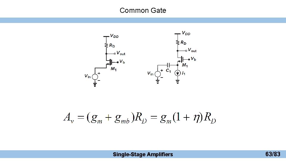
Common Gate Single-Stage Amplifiers 63/83

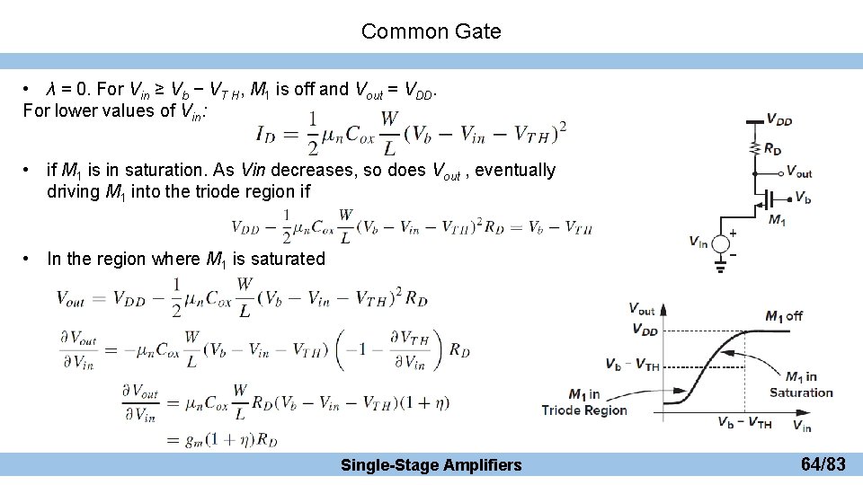
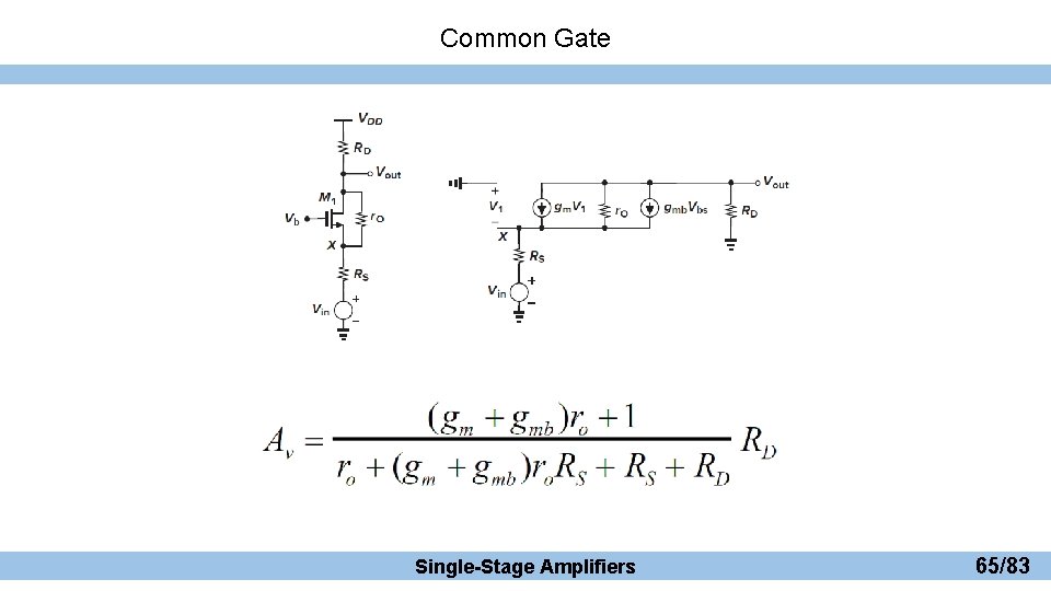
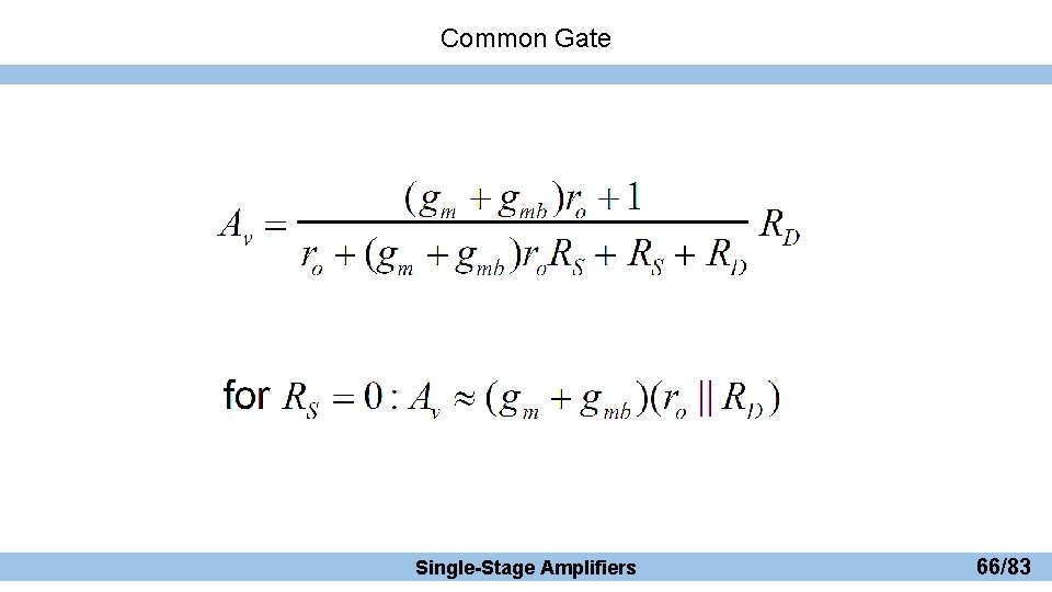
Common Gate • λ = 0. For Vin ≥ Vb − VT H, M 1 is off and Vout = VDD. For lower values of Vin: • if M 1 is in saturation. As Vin decreases, so does Vout , eventually driving M 1 into the triode region if • In the region where M 1 is saturated Single-Stage Amplifiers 64/83

Common Gate Single-Stage Amplifiers 65/83

Common Gate Single-Stage Amplifiers 66/83

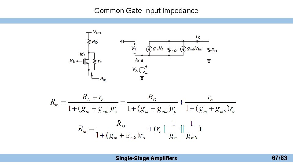
Common Gate Input Impedance Single-Stage Amplifiers 67/83

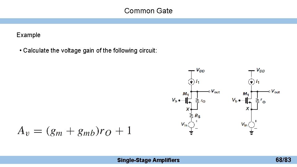
Common Gate Example • Calculate the voltage gain of the following circuit: Single-Stage Amplifiers 68/83

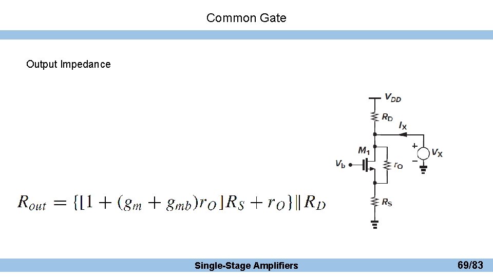
Common Gate Output Impedance Single-Stage Amplifiers 69/83

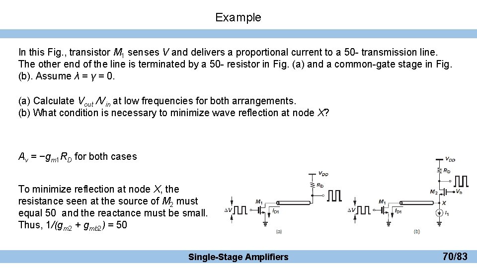
Example In this Fig. , transistor M 1 senses V and delivers a proportional current to a 50 - transmission line. The other end of the line is terminated by a 50 - resistor in Fig. (a) and a common-gate stage in Fig. (b). Assume λ = γ = 0. (a) Calculate Vout /Vin at low frequencies for both arrangements. (b) What condition is necessary to minimize wave reflection at node X? Av = −gm 1 RD for both cases To minimize reflection at node X, the resistance seen at the source of M 2 must equal 50 and the reactance must be small. Thus, 1/(gm 2 + gmb 2) = 50 Single-Stage Amplifiers 70/83

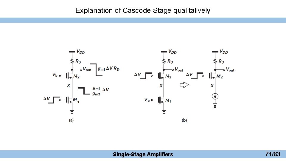
Explanation of Cascode Stage qualitalively Single-Stage Amplifiers 71/83

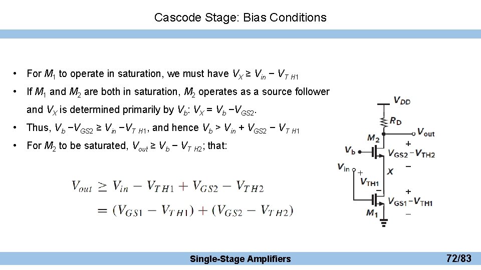
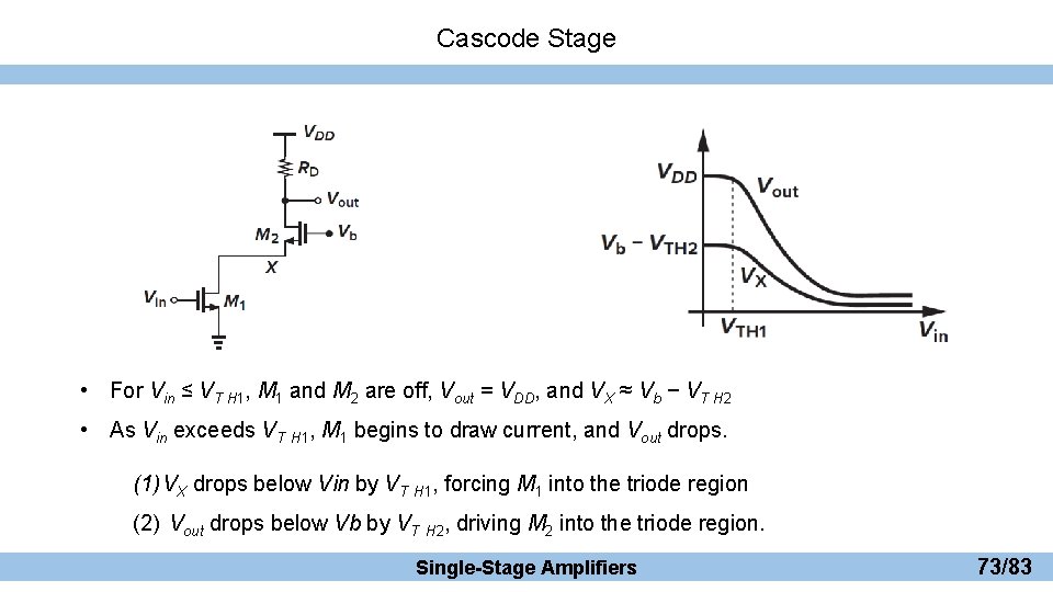
Cascode Stage: Bias Conditions • For M 1 to operate in saturation, we must have VX ≥ Vin − VT H 1 • If M 1 and M 2 are both in saturation, M 2 operates as a source follower and VX is determined primarily by Vb: VX = Vb −VGS 2. • Thus, Vb −VGS 2 ≥ Vin −VT H 1, and hence Vb > Vin + VGS 2 − VT H 1 • For M 2 to be saturated, Vout ≥ Vb − VT H 2; that: Single-Stage Amplifiers 72/83

Cascode Stage • For Vin ≤ VT H 1, M 1 and M 2 are off, Vout = VDD, and VX ≈ Vb − VT H 2 • As Vin exceeds VT H 1, M 1 begins to draw current, and Vout drops. (1) VX drops below Vin by VT H 1, forcing M 1 into the triode region (2) Vout drops below Vb by VT H 2, driving M 2 into the triode region. Single-Stage Amplifiers 73/83

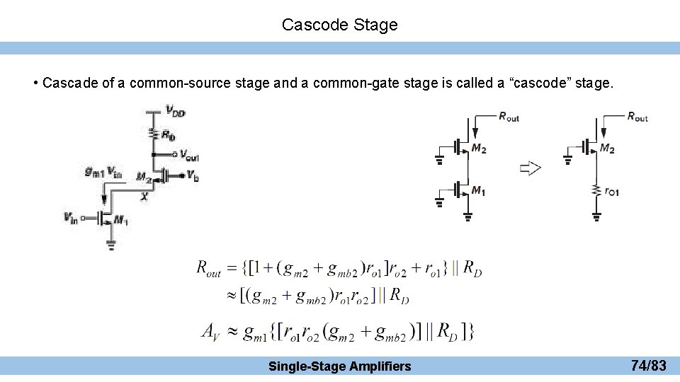
Cascode Stage • Cascade of a common-source stage and a common-gate stage is called a “cascode” stage. Single-Stage Amplifiers 74/83

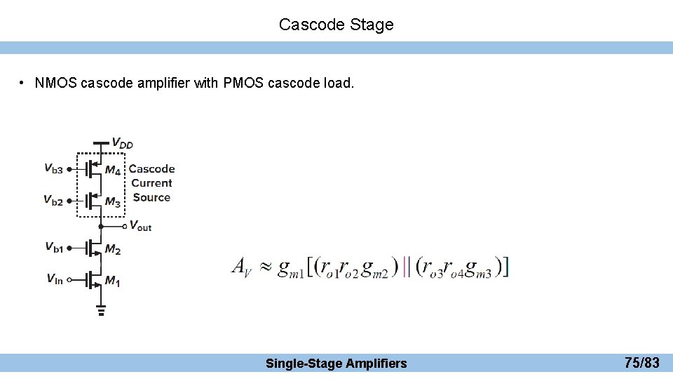
Cascode Stage • NMOS cascode amplifier with PMOS cascode load. Single-Stage Amplifiers 75/83

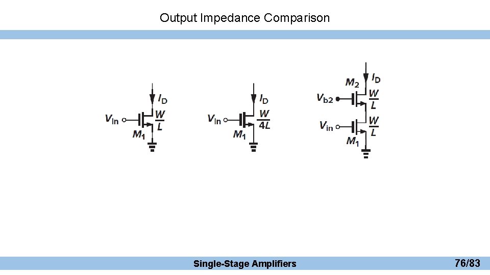
Output Impedance Comparison Single-Stage Amplifiers 76/83

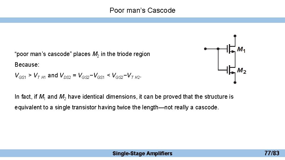
Poor man’s Cascode “poor man’s cascode” places M 2 in the triode region Because: VGS 1 > VT H 1 and VDS 2 = VGS 2−VGS 1 < VGS 2−VT H 2. In fact, if M 1 and M 2 have identical dimensions, it can be proved that the structure is equivalent to a single transistor having twice the length—not really a cascode. Single-Stage Amplifiers 77/83

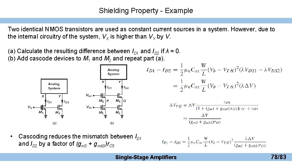
Shielding Property - Example Two identical NMOS transistors are used as constant current sources in a system. However, due to the internal circuitry of the system, VX is higher than VY by V. (a) Calculate the resulting difference between ID 1 and ID 2 if λ = 0. (b) Add cascode devices to M 1 and M 2 and repeat part (a). • Cascoding reduces the mismatch between ID 1 and ID 2 by a factor of (gm 3 + gmb 3)r. O 3 Single-Stage Amplifiers 78/83

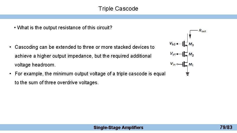
Triple Cascode • What is the output resistance of this circuit? • Cascoding can be extended to three or more stacked devices to achieve a higher output impedance, but the required additional voltage headroom. • For example, the minimum output voltage of a triple cascode is equal to the sum of three overdrive voltages. Single-Stage Amplifiers 79/83

Folded Cascode Single-Stage Amplifiers 80/83

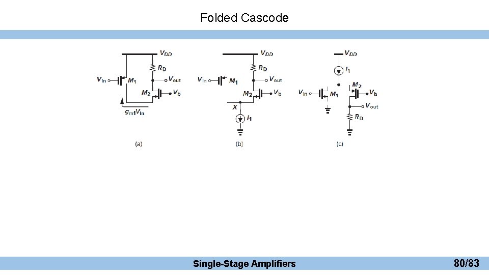
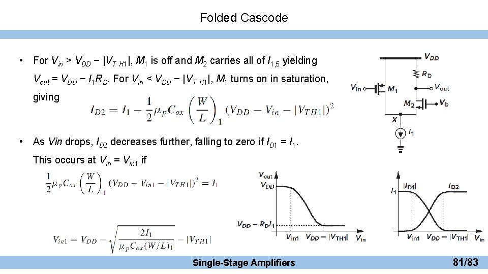
Folded Cascode • For Vin > VDD − |VT H 1|, M 1 is off and M 2 carries all of I 1, 5 yielding Vout = VDD − I 1 RD. For Vin < VDD − |VT H 1|, M 1 turns on in saturation, giving • As Vin drops, ID 2 decreases further, falling to zero if ID 1 = I 1. This occurs at Vin = Vin 1 if Single-Stage Amplifiers 81/83

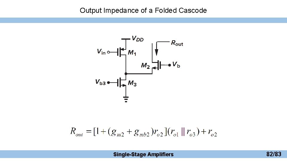
Output Impedance of a Folded Cascode Single-Stage Amplifiers 82/83

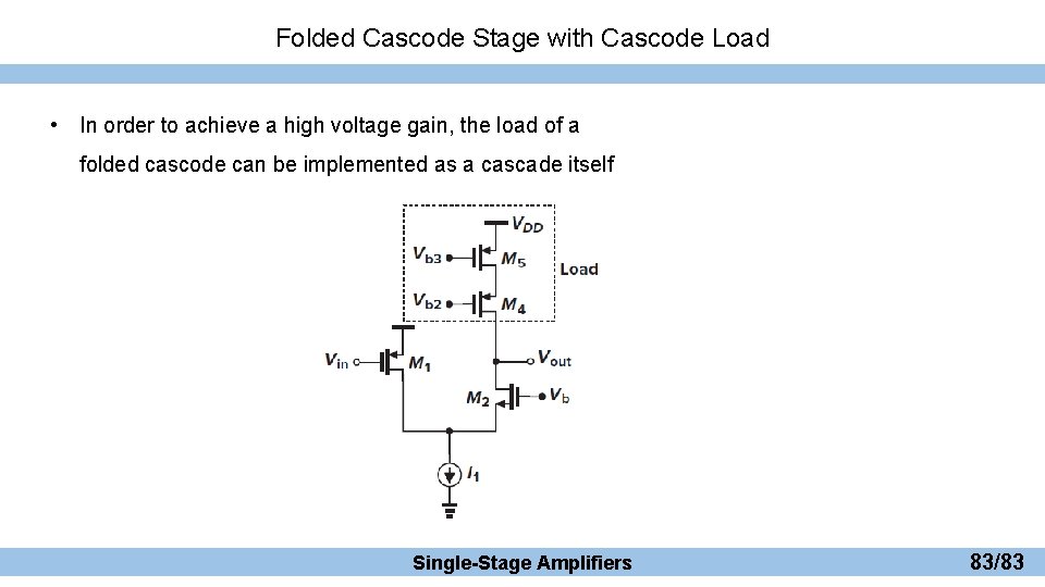
Folded Cascode Stage with Cascode Load • In order to achieve a high voltage gain, the load of a folded cascode can be implemented as a cascade itself Single-Stage Amplifiers 83/83