Analog and RF CMOS circuit design Design of
- Slides: 9

Analog and RF CMOS circuit design Design of a fully integrated wireless power transmitter Alexandre Boyer, Sonia Ben Dhia alexandre. boyer@insa-toulouse. fr www. alexandre-boyer. fr 2017 -2018 135 avenue de Rangueil – 31077 Toulouse cedex 4 – Tel : 05. 61. 55. 95. 13 – Fax : 05. 61. 55. 95. 00 - www. insa-toulouse. fr

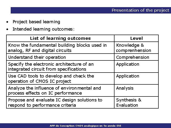
Presentation of the project • Project based learning • Intended learning outcomes: List of learning outcomes Level Know the fundamental building blocks used in analog, RF and digital circuits Knowledge & comprenhension Understand their operation Comprehension Specify the electronic architecture of an integrated circuit from specifications Application Use CAD tools to develop and check the operation of CMOS IC project Application Analyze the influence of environmental and process effects on IC performance Analysis Propose and evaluate IC design solutions to respond to performance criteria Synthesis & Evaluation APP de Conception CMOS analogique en 5 e année ESE

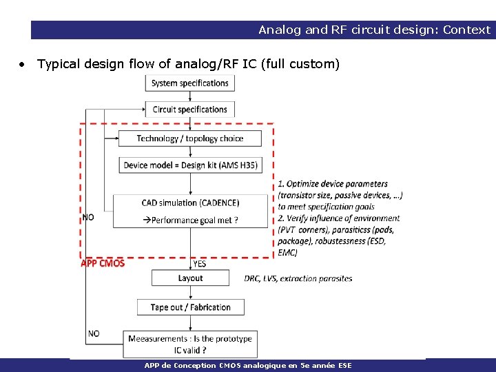
Analog and RF circuit design: Context • Typical design flow of analog/RF IC (full custom) APP de Conception CMOS analogique en 5 e année ESE

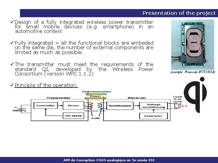
Presentation of the project ü Design of a fully integrated wireless power transmitter for small mobile devices (e. g. smartphone) in an automotive context ü Fully integrated = all the functional blocks are embeded on the same die, the number of external components are limited as much as possible. ü The transmitter must meet the requirements of the standard QI, developed by the Wireless Power Consortium (version WPC 1. 1. 2) ü Principle of the operation: APP de Conception CMOS analogique en 5 e année ESE (example: Freescale WCT 1001 A)

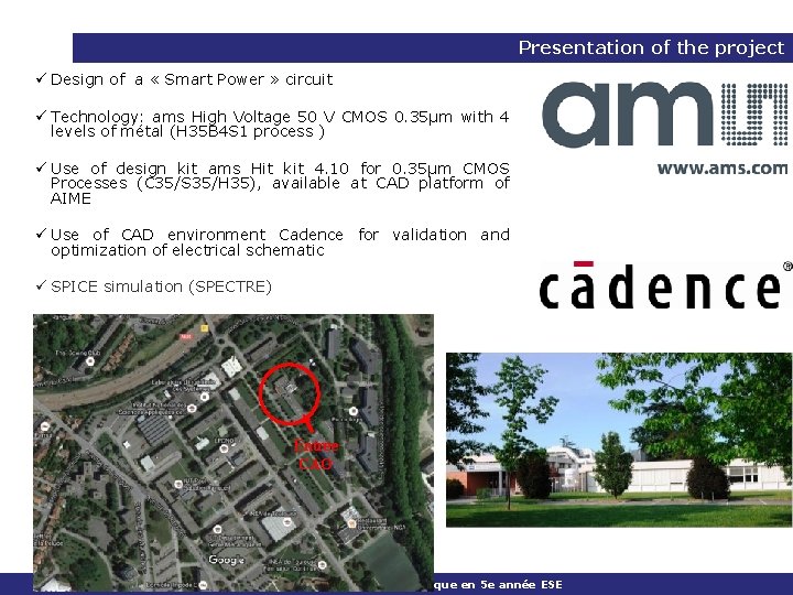
Presentation of the project ü Design of a « Smart Power » circuit ü Technology: ams High Voltage 50 V CMOS 0. 35µm with 4 levels of métal (H 35 B 4 S 1 process ) ü Use of design kit ams Hit kit 4. 10 for 0. 35µm CMOS Processes (C 35/S 35/H 35), available at CAD platform of AIME ü Use of CAD environment Cadence for validation and optimization of electrical schematic ü SPICE simulation (SPECTRE) Entrée CAO APP de Conception CMOS analogique en 5 e année ESE

Presentation of the project • Main steps of the project: 1. Design an architecture of the circuit (block diagram) with all the physical inputoutputs 2. Respect all the constraints (functional performances, electrical, environmental, technological constraints, etc. ) 3. Propose electrical diagram of some analog/RF blocks of the circuits with associated constraints 4. Write a specifications report containing the previous information 5. Validation and improvement of electrical schematic based on CAD tool (Cadence) 6. Prediction of circuit performances in the different PVT conditions 7. Write a design report ( « scientific paper » format) which presents the designed circuit and simulated performances APP de Conception CMOS analogique en 5 e année ESE

Presentation of the project üList of specifications in Analog_CMOS_Design_Project_2017 -18. pdf üLink with English course. üList of documents available boyer. fr/enseignements. htm (link to specifications, students reports) on www. alexandrecourses, technological üAssessments by two written reports and a final presentation: 1. Detailed circuit specification (Specification_report_WPT_Gpe. X_2016. doc) Due before Friday 10/11/2017 at 23 h 59 2. Design report (Fiche synthese English version. doc) Due before Tuesday 09/01/2018 at 23 h 59 3. Final presentations (during English course) Wednesday 17/01/2018 afternoon APP de Conception CMOS analogique en 5 e année ESE

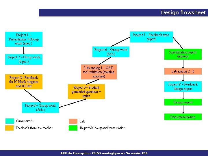
Design flowsheet Project 7 – Feedback spec. report Project 1 – Presentation + Group work (spec. ) Project 6 – Group work (Sch. ) Project 2 – Group work (Spec. ) Project 3– Feedback for IC block diagram and I/O list Lab analog 1 – CAD tool initiation (starting exercise) Project 5– Student generated question + quizz Specification report delivery Lab analog 2 - 6 Project 8 – Feedback design report Design report Project 4– Group work (Sch. ) Final presentation Group work Lab Feedback from the teacher Report delivery and presentation APP de Conception CMOS analogique en 5 e année ESE

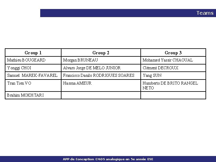
Teams Group 1 Group 2 Group 3 Mathieu BOUGEARD Morgan BRUNEAU Mohamed Yassir CHAOUAL Yonggi CHOI Alvaro Jorge DE MELO JUNIOR Clément DECROUX Samuel MAREK-FAVAREL Francisco Danilo RODRIGUES SOARES Yang SUN Tran Tien VO Hassna AMEUR Humberto DE BRITO RANGEL NETO Brahim MOKHTARI APP de Conception CMOS analogique en 5 e année ESE