MOS FieldEffect Transistors MOSFETs 1 Figure 4 1
- Slides: 10
MOS Field-Effect Transistors (MOSFETs) 1
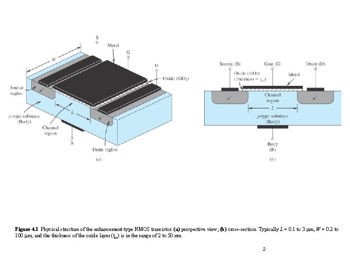
Figure 4. 1 Physical structure of the enhancement-type NMOS transistor: (a) perspective view; (b) cross-section. Typically L = 0. 1 to 3 mm, W = 0. 2 to 100 mm, and the thickness of the oxide layer (tox) is in the range of 2 to 50 nm. 2
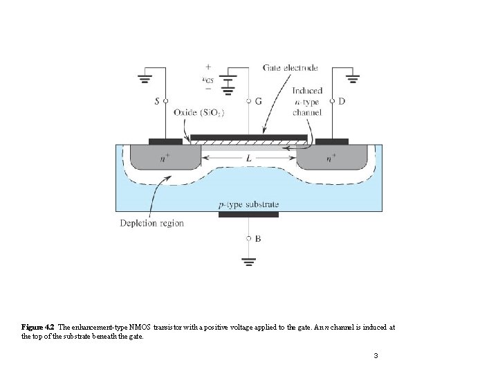
Figure 4. 2 The enhancement-type NMOS transistor with a positive voltage applied to the gate. An n channel is induced at the top of the substrate beneath the gate. 3
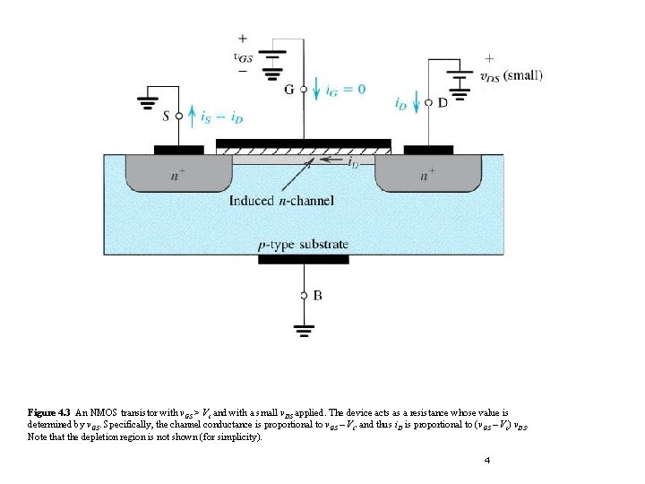
Figure 4. 3 An NMOS transistor with v. GS > Vt and with a small v. DS applied. The device acts as a resistance whose value is determined by v. GS. Specifically, the channel conductance is proportional to v. GS – Vt’ and thus i. D is proportional to (v. GS – Vt) v. DS. Note that the depletion region is not shown (for simplicity). 4
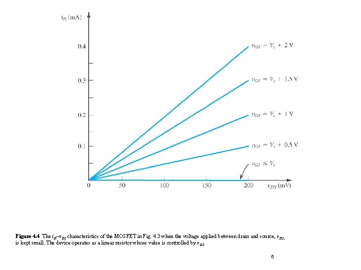
Figure 4. 4 The i. D–v. DS characteristics of the MOSFET in Fig. 4. 3 when the voltage applied between drain and source, v. DS, is kept small. The device operates as a linear resistor whose value is controlled by v. GS. 5
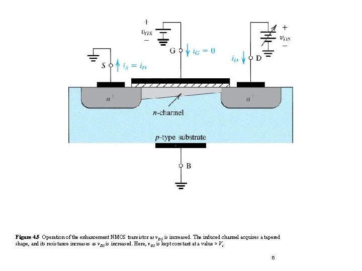
Figure 4. 5 Operation of the enhancement NMOS transistor as v. DS is increased. The induced channel acquires a tapered shape, and its resistance increases as v. DS is increased. Here, v. GS is kept constant at a value > Vt. 6
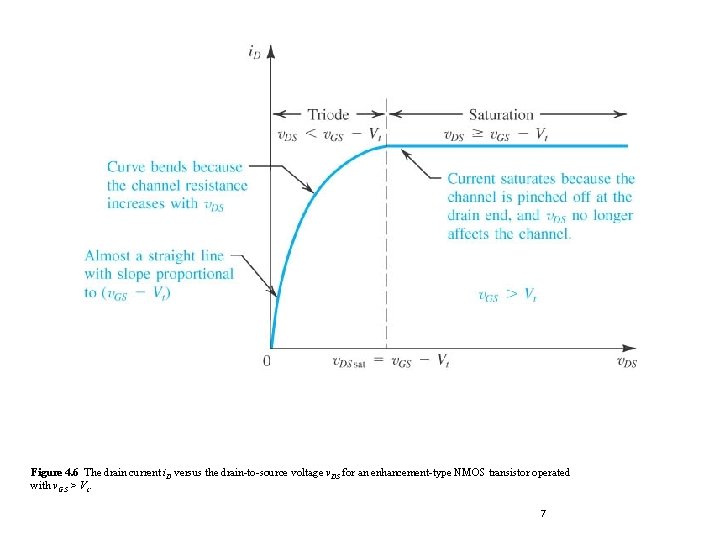
Figure 4. 6 The drain current i. D versus the drain-to-source voltage v. DS for an enhancement-type NMOS transistor operated with v. GS > Vt. 7
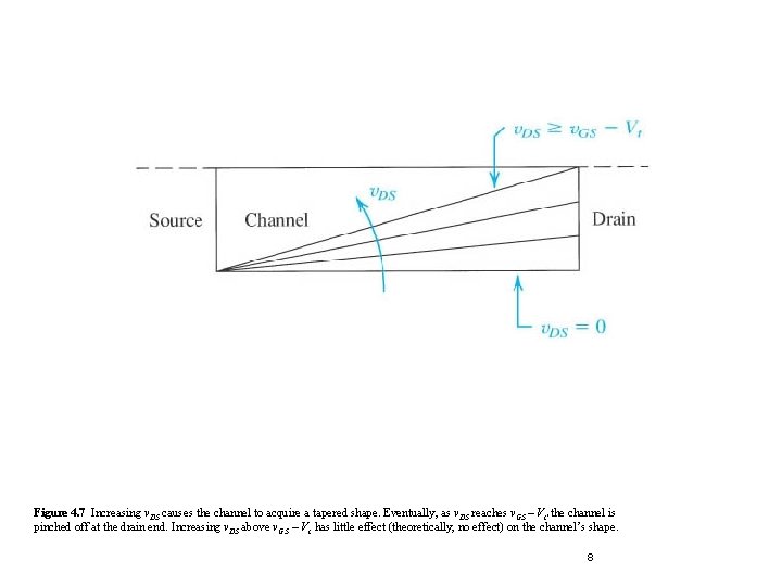
Figure 4. 7 Increasing v. DS causes the channel to acquire a tapered shape. Eventually, as v. DS reaches v. GS – Vt’ the channel is pinched off at the drain end. Increasing v. DS above v. GS – Vt has little effect (theoretically, no effect) on the channel’s shape. 8
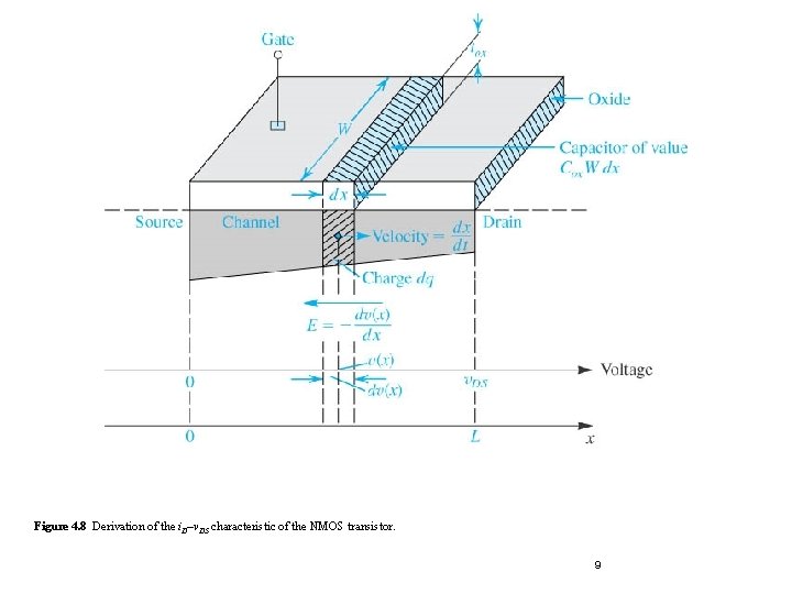
Figure 4. 8 Derivation of the i. D–v. DS characteristic of the NMOS transistor. 9
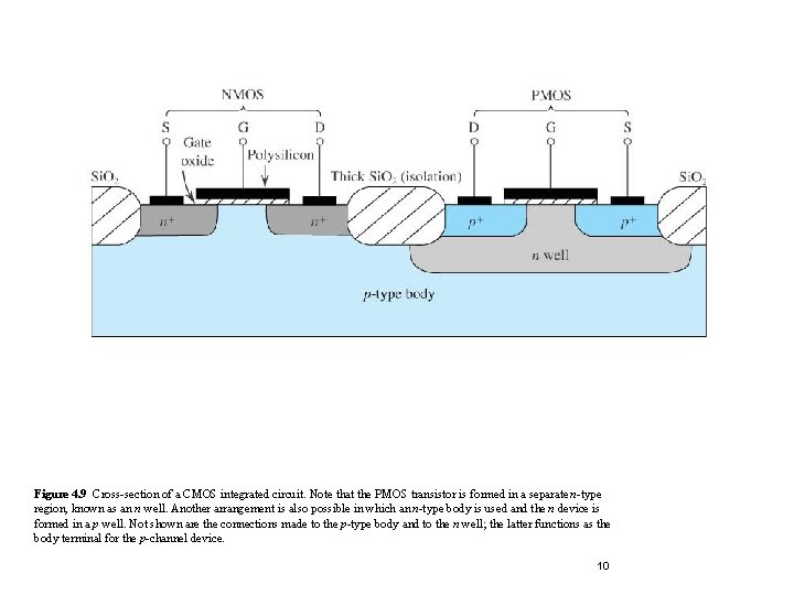
Figure 4. 9 Cross-section of a CMOS integrated circuit. Note that the PMOS transistor is formed in a separate n-type region, known as an n well. Another arrangement is also possible in which an n-type body is used and the n device is formed in a p well. Not shown are the connections made to the p-type body and to the n well; the latter functions as the body terminal for the p-channel device. 10