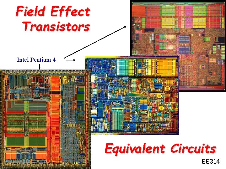
Field Effect Transistors Intel Pentium 4 Equivalent Circuits


- Slides: 16

Field Effect Transistors Intel Pentium 4 Equivalent Circuits EE 314

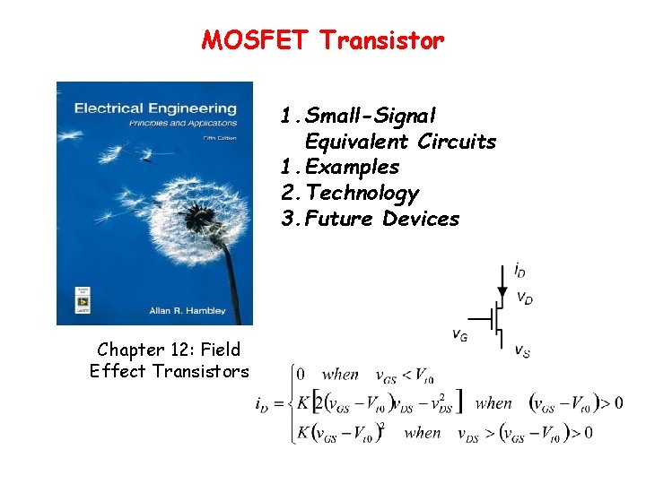
MOSFET Transistor 1. Small-Signal Equivalent Circuits 1. Examples 2. Technology 3. Future Devices Chapter 12: Field Effect Transistors

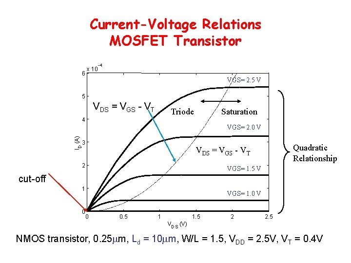
Current-Voltage Relations MOSFET Transistor 6 x 10 -4 VGS= 2. 5 VDS = VGS - VT Triode Saturation 4 ID (A) VGS= 2. 0 V 3 Quadratic Relationship VDS = VGS - VT 2 VGS= 1. 5 V cut-off 1 0 VGS= 1. 0 V 0 0. 5 1 1. 5 2 2. 5 VDS (V) NMOS transistor, 0. 25 mm, Ld = 10 mm, W/L = 1. 5, VDD = 2. 5 V, VT = 0. 4 V

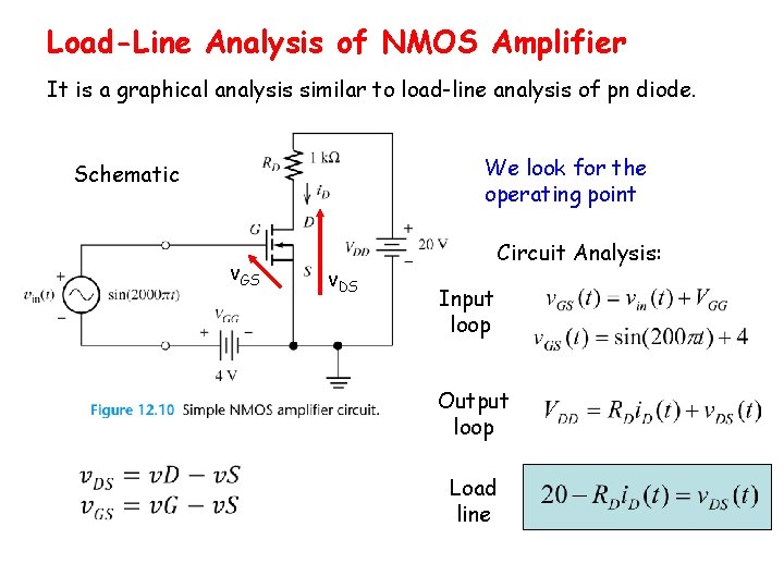
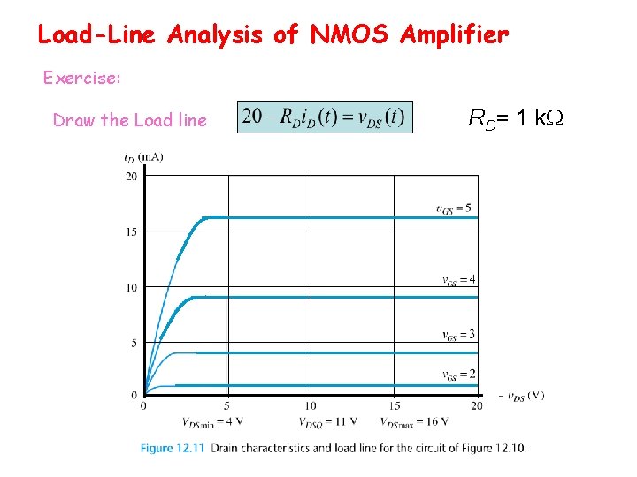
Load-Line Analysis of NMOS Amplifier It is a graphical analysis similar to load-line analysis of pn diode. We look for the operating point Schematic v. GS v. DS Circuit Analysis: Input loop Output loop Load line

Load-Line Analysis of NMOS Amplifier Exercise: Draw the Load line RD= 1 k. W

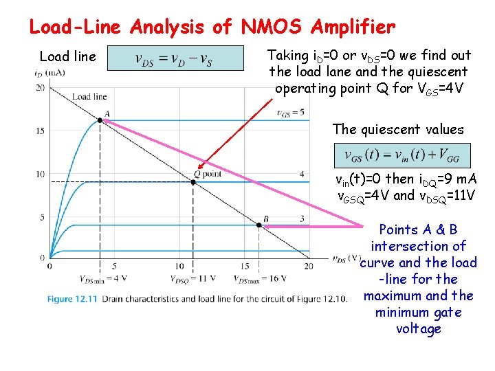
Load-Line Analysis of NMOS Amplifier Load line Taking i. D=0 or v. DS=0 we find out the load lane and the quiescent operating point Q for VGS=4 V The quiescent values vin(t)=0 then i. DQ=9 m. A v. GSQ=4 V and v. DSQ=11 V Points A & B intersection of curve and the load -line for the maximum and the minimum gate voltage

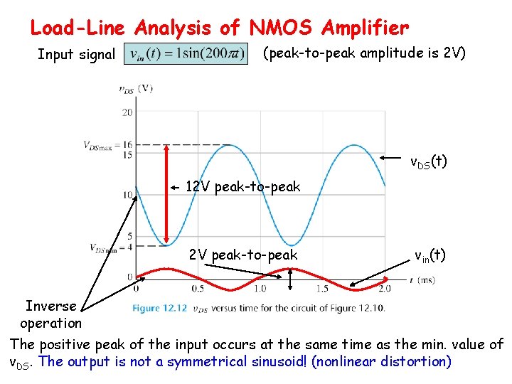
Load-Line Analysis of NMOS Amplifier Input signal (peak-to-peak amplitude is 2 V) v. DS(t) 12 V peak-to-peak vin(t) Inverse operation The positive peak of the input occurs at the same time as the min. value of v. DS. The output is not a symmetrical sinusoid! (nonlinear distortion)

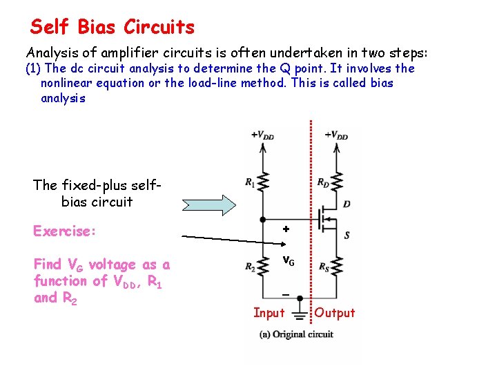
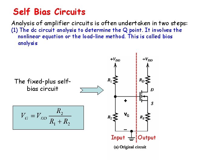
Self Bias Circuits Analysis of amplifier circuits is often undertaken in two steps: (1) The dc circuit analysis to determine the Q point. It involves the nonlinear equation or the load-line method. This is called bias analysis The fixed-plus selfbias circuit Exercise: + Find VG voltage as a function of VDD, R 1 and R 2 v. G _ Input Output

Self Bias Circuits Analysis of amplifier circuits is often undertaken in two steps: (1) The dc circuit analysis to determine the Q point. It involves the nonlinear equation or the load-line method. This is called bias analysis The fixed-plus selfbias circuit + v. G _ Input Output

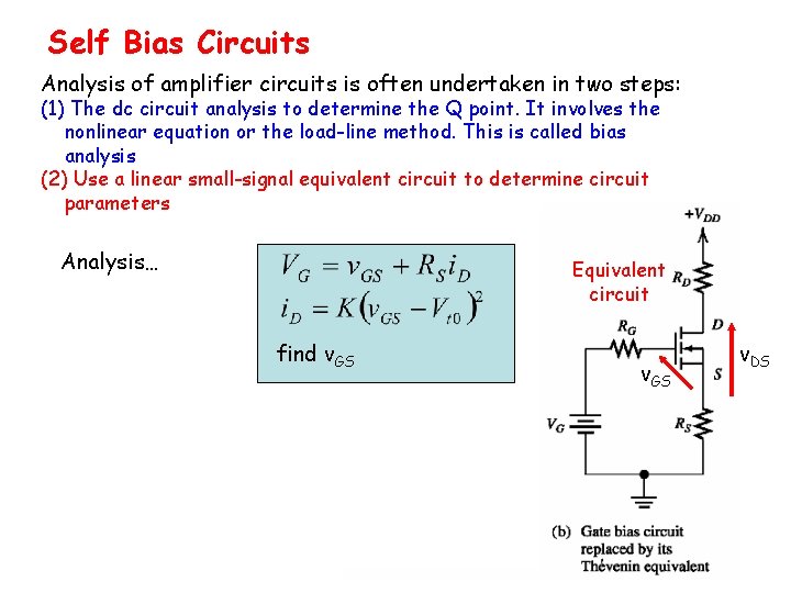
Self Bias Circuits Analysis of amplifier circuits is often undertaken in two steps: (1) The dc circuit analysis to determine the Q point. It involves the nonlinear equation or the load-line method. This is called bias analysis (2) Use a linear small-signal equivalent circuit to determine circuit parameters Analysis… Equivalent circuit find v. GS v. DS

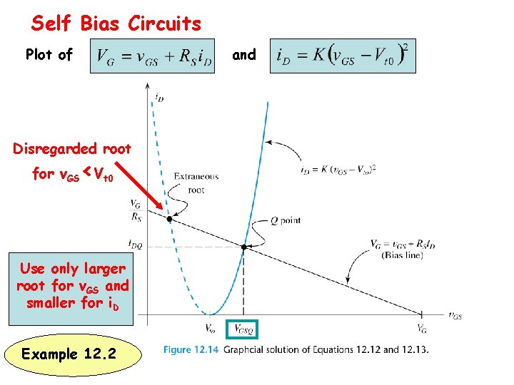
Self Bias Circuits Plot of and Disregarded root < for v. GS Vt 0 Use only larger root for v. GS and smaller for i. D Example 12. 2

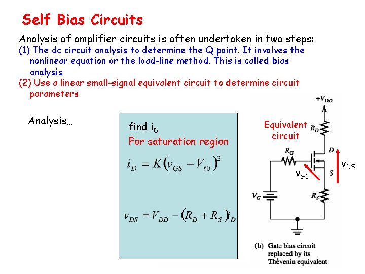
Self Bias Circuits Analysis of amplifier circuits is often undertaken in two steps: (1) The dc circuit analysis to determine the Q point. It involves the nonlinear equation or the load-line method. This is called bias analysis (2) Use a linear small-signal equivalent circuit to determine circuit parameters Analysis… find i. D For saturation region Equivalent circuit v. GS v. DS

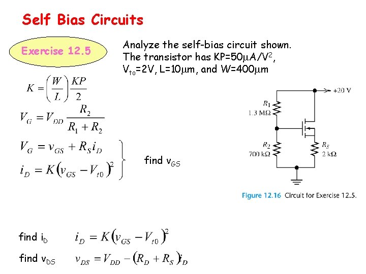
Self Bias Circuits Exercise 12. 5 Analyze the self-bias circuit shown. The transistor has KP=50 m. A/V 2, Vto=2 V, L=10 mm, and W=400 mm find v. GS find i. D find v. DS

Flexible Field Effect Transistors EE 314

Play video about plastic electronics http: //www. plasticlogic. com Q: How we can do this? A: A new generation of MOSFETs for plastic electronics

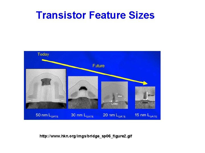
Transistor Feature Sizes http: //www. hkn. org/imgs/bridge_sp 06_figure 2. gif