Design and optimization of Schottky diodes in CMOS



- Slides: 20

Design and optimization of Schottky diodes in CMOS technology with application to passive RFID systems Auto-ID lab Adelaide

Overview • Introduction. • Design and layout of Schottky diode. • Modelling of designed SBD. • Applications. • Fabrication and measurements. • Conclusion.

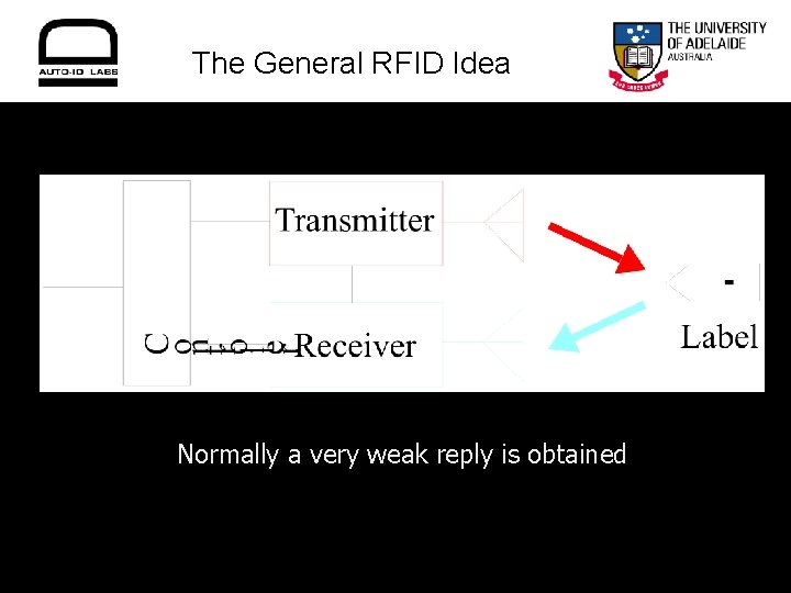
The General RFID Idea The black spot Normally a very weak reply is obtained

Example Applications • What can you do with this technology ? Supply chain benefits – Reduce out of stocks, reduce inventory, speed up delivery, check freshness, track and trace, produce to demand, identify sources of diversion, identify counterfeiting, theft prediction, faster recalls Consumer benefits – Direct order from home, smart appliances, (e. g. microwave, washing machine, refrigerator), smart healthcare, assisted living New and less expected benefits – Customized products, smart recycling, checkout-less stores

Passive RFID • RFID tag chip in standard CMOS technology. Low size. Low cost. Integration with existing logics and other modules. • Supply sufficient operating power • Metal directly deposited on N-Well. • Titanium-Silicon/Tungsten-Silicon contact • Functional but needs more improvements. Fabricated through MOSIS

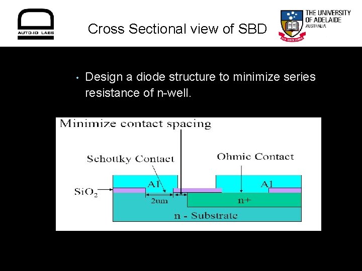
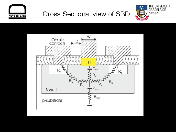
Cross Sectional view of SBD • Design a diode structure to minimize series resistance of n-well.

Cross Sectional view of SBD

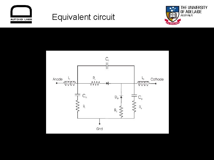
Equivalent circuit

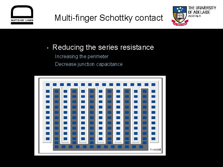
Multi-finger Schottky contact • Reducing the series resistance Increasing the perimeter Decrease junction capacitance

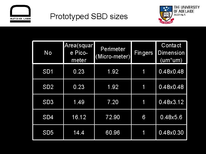
Prototyped SBD sizes No Area(squar Contact Perimeter e Pico. Fingers Dimension (Micro-meter) meter (um*um) SD 1 0. 23 1. 92 1 0. 48 x 0. 48 SD 2 0. 23 1. 92 1 0. 48 x 0. 48 SD 3 1. 49 7. 20 1 0. 48 x 3. 12 SD 4 16. 12 72. 90 6 0. 48 x 5. 6 SD 5 14. 4 60. 96 1 0. 48 x 0. 30

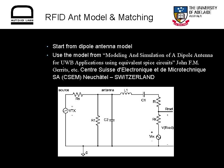
RFID Ant Model & Matching • Start from dipole antenna model • Use the model from “Modeling And Simulation of A Dipole Antenna for UWB Applications using equivalent spice circuits” John F. M. Gerrits, etc. Centre Suisse d'Electronique et de Microtechnique SA (CSEM) Neuchâtel – SWITZERLAND

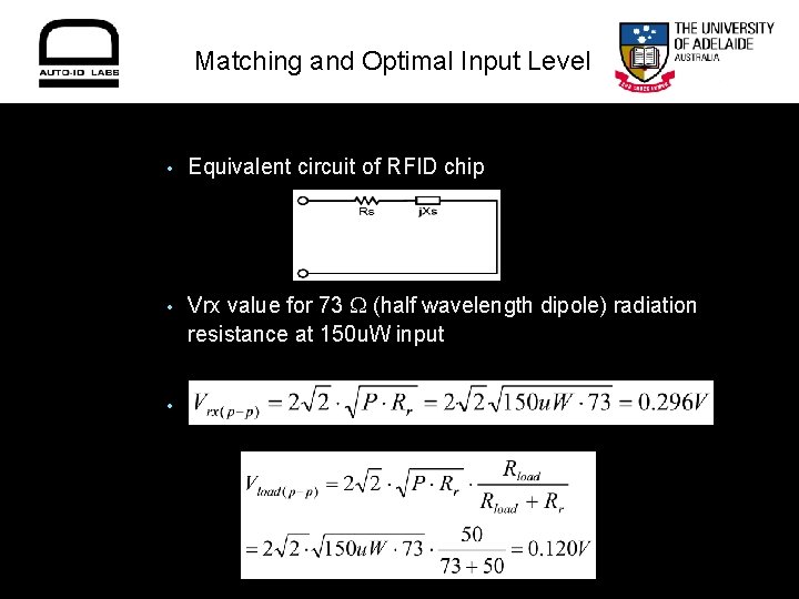
Matching and Optimal Input Level • Equivalent circuit of RFID chip • Vrx value for 73 (half wavelength dipole) radiation resistance at 150 u. W input • 50 resistor voltage swing

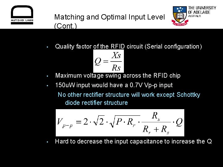
Matching and Optimal Input Level (Cont. ) • Quality factor of the RFID circuit (Serial configuration) • Maximum voltage swing across the RFID chip • 150 u. W input would have a 0. 7 V Vp-p input No other rectifier structure will work except Schottky diode rectifier structure • Hard to decrease the input capacitance to increase the Q

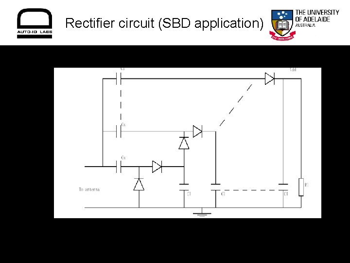
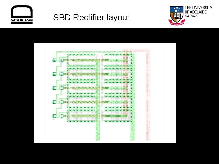
Rectifier circuit (SBD application)

SBD Rectifier layout

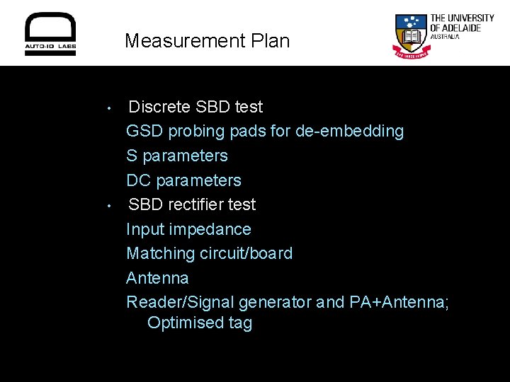
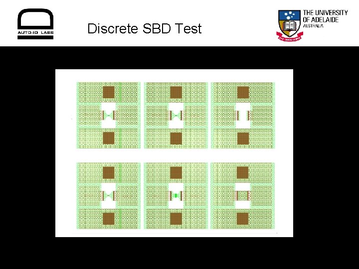
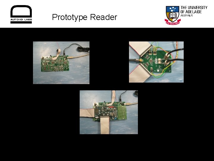
Measurement Plan • • Discrete SBD test GSD probing pads for de-embedding S parameters DC parameters SBD rectifier test Input impedance Matching circuit/board Antenna Reader/Signal generator and PA+Antenna; Optimised tag

Discrete SBD Test

Prototype Reader

Future Work • Test and extract the model parameters • Validating the SBD model • Improve the quality factor of the SBD • Increase reverse direction breakdown voltage by guard ring (fabricated version dose not have) • Improve efficiency by reducing parasitic capacitance • Better impedance matching capabilities

Q&A • Thank You