Chapter 3 SolidState Diodes and Diode Circuits Microelectronic









- Slides: 95

Chapter 3 Solid-State Diodes and Diode Circuits Microelectronic Circuit Design Richard C. Jaeger Travis N. Blalock Jaeger/Blalock 7/1/03 Microelectronic Circuit Design Mc. Graw-Hill Chap 3 -1

Chapter Goals • Understand diode structure and basic layout • Develop electrostatics of the pn junction • Explore various diode models including the mathematical model, the ideal diode model, and the constant voltage drop model • Understand the SPICE representation and model parameters for the diode • Define regions of operation of the diode (forward, reverse bias, and reverse breakdown) • Apply the various types of models in circuit analysis • Explore different types of diodes Discuss the dynamic switching behavior of the pn junction diode • Explore diode applications • Practice simulating diode circuits using SPICE Jaeger/Blalock 7/1/03 Microelectronic Circuit Design Mc. Graw-Hill Chap 3 -2

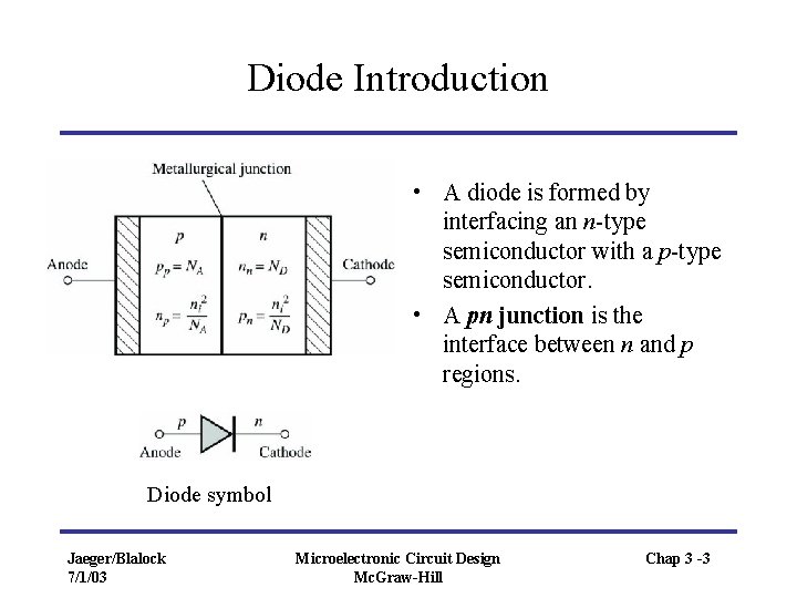
Diode Introduction • A diode is formed by interfacing an n-type semiconductor with a p-type semiconductor. • A pn junction is the interface between n and p regions. Diode symbol Jaeger/Blalock 7/1/03 Microelectronic Circuit Design Mc. Graw-Hill Chap 3 -3

PN Junction Animation • Formation of PN Junction – applet • PN Junction space charge profile and electric field – applet • Biased PN Junction - applet Jaeger/Blalock 7/1/03 Microelectronic Circuit Design Mc. Graw-Hill

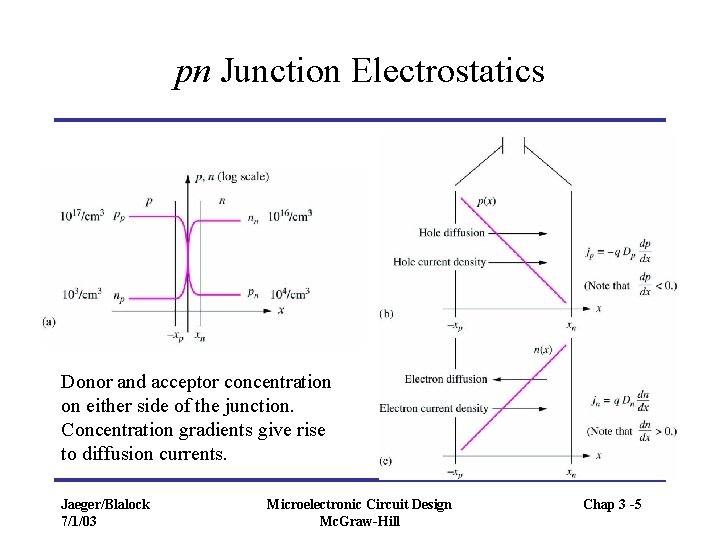
pn Junction Electrostatics Donor and acceptor concentration on either side of the junction. Concentration gradients give rise to diffusion currents. Jaeger/Blalock 7/1/03 Microelectronic Circuit Design Mc. Graw-Hill Chap 3 -5

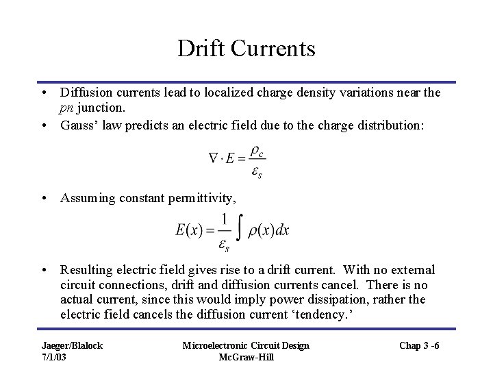
Drift Currents • Diffusion currents lead to localized charge density variations near the pn junction. • Gauss’ law predicts an electric field due to the charge distribution: • Assuming constant permittivity, • Resulting electric field gives rise to a drift current. With no external circuit connections, drift and diffusion currents cancel. There is no actual current, since this would imply power dissipation, rather the electric field cancels the diffusion current ‘tendency. ’ Jaeger/Blalock 7/1/03 Microelectronic Circuit Design Mc. Graw-Hill Chap 3 -6

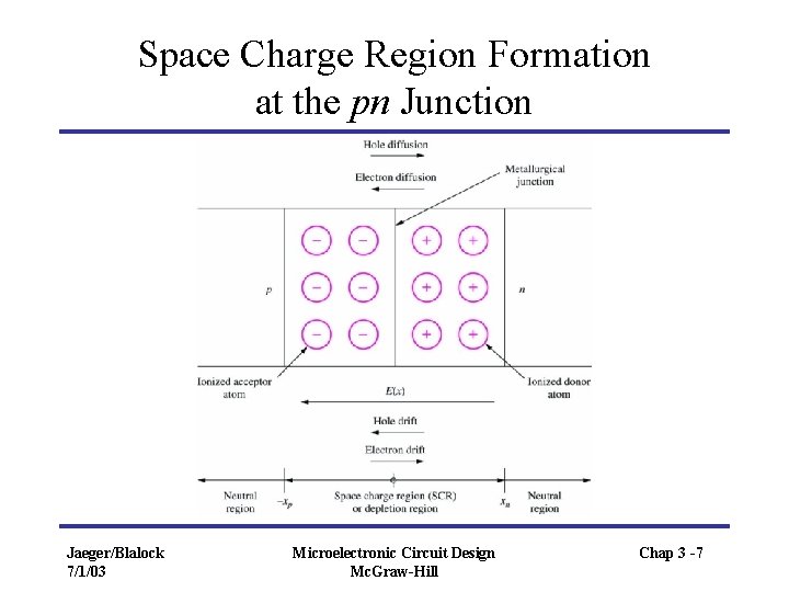
Space Charge Region Formation at the pn Junction Jaeger/Blalock 7/1/03 Microelectronic Circuit Design Mc. Graw-Hill Chap 3 -7

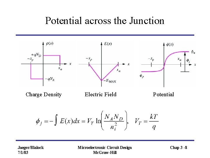
Potential across the Junction Charge Density Jaeger/Blalock 7/1/03 Electric Field Microelectronic Circuit Design Mc. Graw-Hill Potential Chap 3 -8

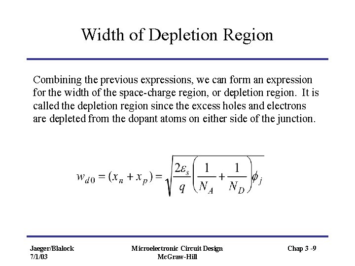
Width of Depletion Region Combining the previous expressions, we can form an expression for the width of the space-charge region, or depletion region. It is called the depletion region since the excess holes and electrons are depleted from the dopant atoms on either side of the junction. Jaeger/Blalock 7/1/03 Microelectronic Circuit Design Mc. Graw-Hill Chap 3 -9

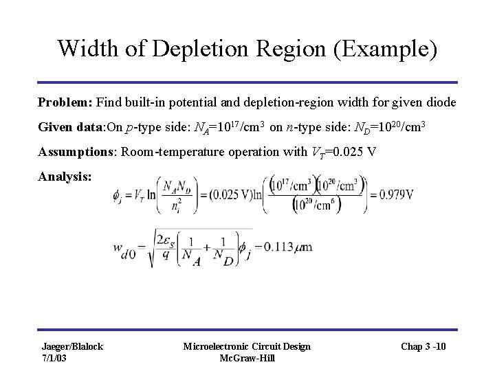
Width of Depletion Region (Example) Problem: Find built-in potential and depletion-region width for given diode Given data: On p-type side: NA=1017/cm 3 on n-type side: ND=1020/cm 3 Assumptions: Room-temperature operation with VT=0. 025 V Analysis: Jaeger/Blalock 7/1/03 Microelectronic Circuit Design Mc. Graw-Hill Chap 3 -10

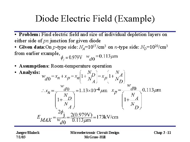
Diode Electric Field (Example) • Problem: Find electric field and size of individual depletion layers on either side of pn junction for given diode • Given data: On p-type side: NA=1017/cm 3 on n-type side: ND=1020/cm 3 from earlier example, • Assumptions: Room-temperature operation • Analysis: Jaeger/Blalock 7/1/03 Microelectronic Circuit Design Mc. Graw-Hill Chap 3 -11

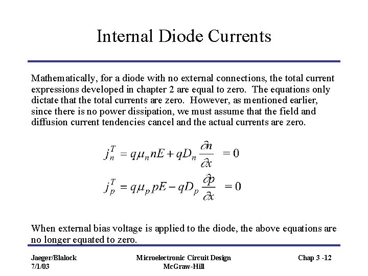
Internal Diode Currents Mathematically, for a diode with no external connections, the total current expressions developed in chapter 2 are equal to zero. The equations only dictate that the total currents are zero. However, as mentioned earlier, since there is no power dissipation, we must assume that the field and diffusion current tendencies cancel and the actual currents are zero. When external bias voltage is applied to the diode, the above equations are no longer equated to zero. Jaeger/Blalock 7/1/03 Microelectronic Circuit Design Mc. Graw-Hill Chap 3 -12

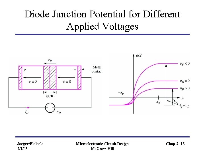
Diode Junction Potential for Different Applied Voltages Jaeger/Blalock 7/1/03 Microelectronic Circuit Design Mc. Graw-Hill Chap 3 -13

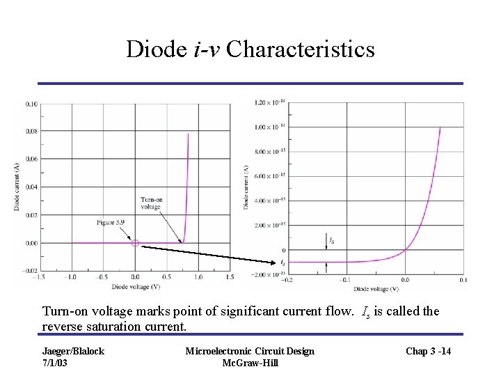
Diode i-v Characteristics Turn-on voltage marks point of significant current flow. Is is called the reverse saturation current. Jaeger/Blalock 7/1/03 Microelectronic Circuit Design Mc. Graw-Hill Chap 3 -14

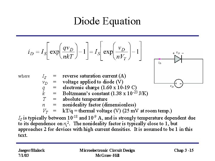
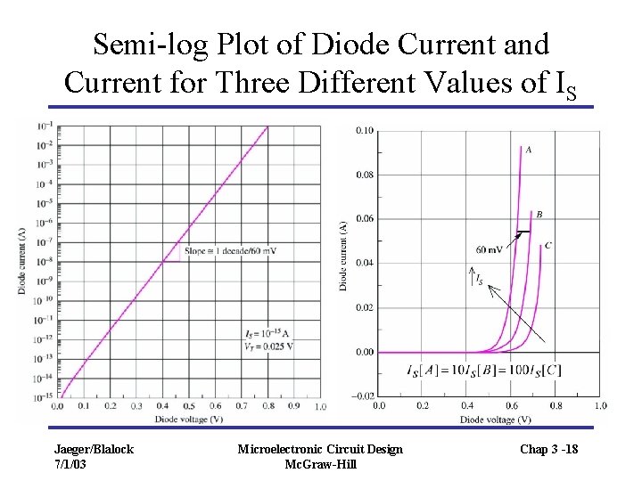
Diode Equation = reverse saturation current (A) v. D = voltage applied to diode (V) q = electronic charge (1. 60 x 10 -19 C) k = Boltzmann’s constant (1. 38 x 10 -23 J/K) T = absolute temperature n = nonideality factor (dimensionless) VT = k. T/q = thermal voltage (V) (25 m. V at room temp. ) IS is typically between 10 -18 and 10 -9 A, and is strongly temperature dependent due to its dependence on ni 2. The nonideality factor is typically close to 1, but approaches 2 for devices with high current densities. It is assumed to be 1 in this text. where IS Jaeger/Blalock 7/1/03 Microelectronic Circuit Design Mc. Graw-Hill Chap 3 -15

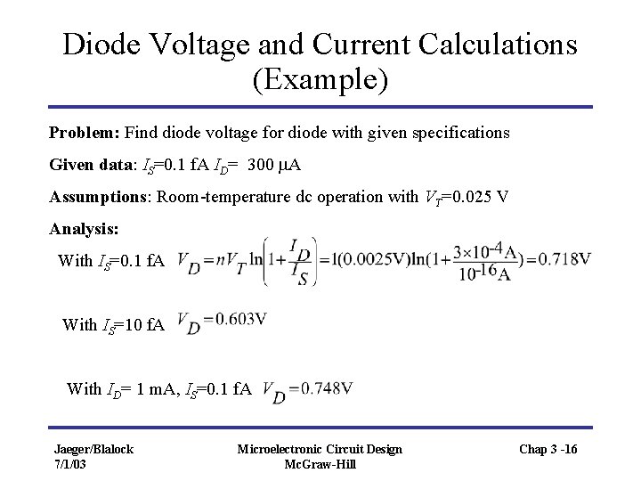
Diode Voltage and Current Calculations (Example) Problem: Find diode voltage for diode with given specifications Given data: IS=0. 1 f. A ID= 300 m. A Assumptions: Room-temperature dc operation with VT=0. 025 V Analysis: With IS=0. 1 f. A With IS=10 f. A With ID= 1 m. A, IS=0. 1 f. A Jaeger/Blalock 7/1/03 Microelectronic Circuit Design Mc. Graw-Hill Chap 3 -16

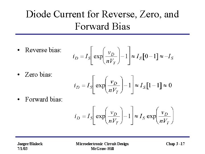
Diode Current for Reverse, Zero, and Forward Bias • Reverse bias: • Zero bias: • Forward bias: Jaeger/Blalock 7/1/03 Microelectronic Circuit Design Mc. Graw-Hill Chap 3 -17

Semi-log Plot of Diode Current and Current for Three Different Values of IS Jaeger/Blalock 7/1/03 Microelectronic Circuit Design Mc. Graw-Hill Chap 3 -18

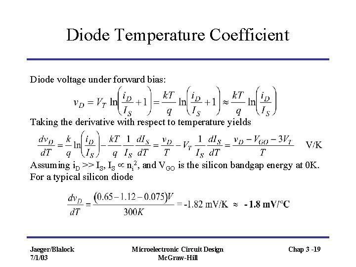
Diode Temperature Coefficient Diode voltage under forward bias: Taking the derivative with respect to temperature yields Assuming i. D >> IS, IS ni 2, and VGO is the silicon bandgap energy at 0 K. For a typical silicon diode Jaeger/Blalock 7/1/03 Microelectronic Circuit Design Mc. Graw-Hill Chap 3 -19

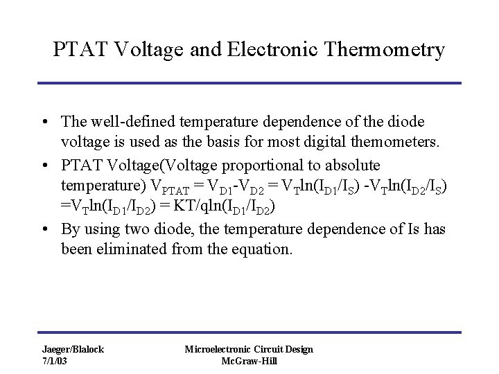
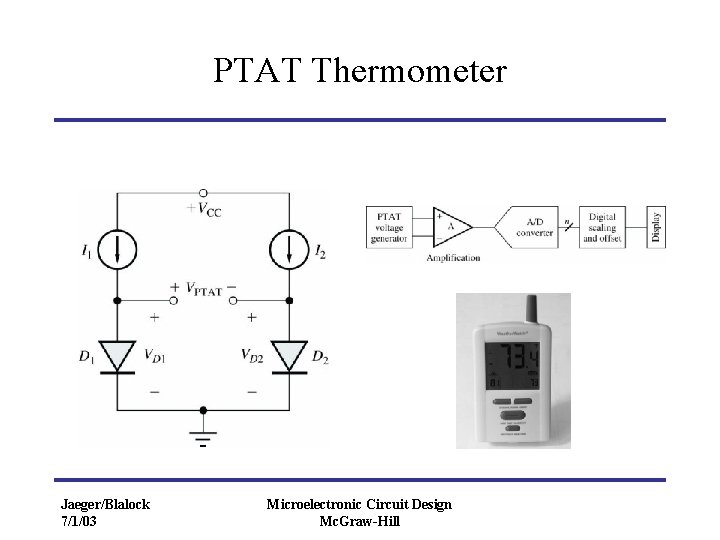
PTAT Voltage and Electronic Thermometry • The well-defined temperature dependence of the diode voltage is used as the basis for most digital themometers. • PTAT Voltage(Voltage proportional to absolute temperature) VPTAT = VD 1 -VD 2 = VTln(ID 1/IS) -VTln(ID 2/IS) =VTln(ID 1/ID 2) = KT/qln(ID 1/ID 2) • By using two diode, the temperature dependence of Is has been eliminated from the equation. Jaeger/Blalock 7/1/03 Microelectronic Circuit Design Mc. Graw-Hill

PTAT Thermometer Jaeger/Blalock 7/1/03 Microelectronic Circuit Design Mc. Graw-Hill

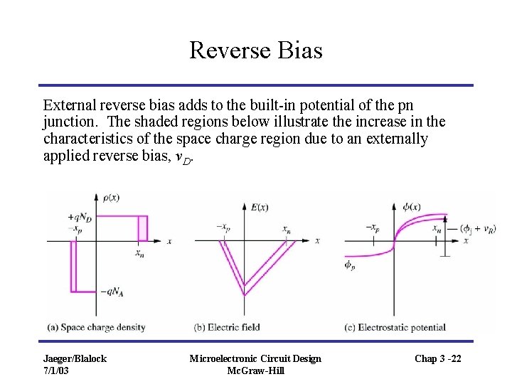
Reverse Bias External reverse bias adds to the built-in potential of the pn junction. The shaded regions below illustrate the increase in the characteristics of the space charge region due to an externally applied reverse bias, v. D. Jaeger/Blalock 7/1/03 Microelectronic Circuit Design Mc. Graw-Hill Chap 3 -22

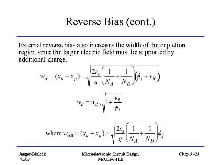
Reverse Bias (cont. ) External reverse bias also increases the width of the depletion region since the larger electric field must be supported by additional charge. Jaeger/Blalock 7/1/03 Microelectronic Circuit Design Mc. Graw-Hill Chap 3 -23

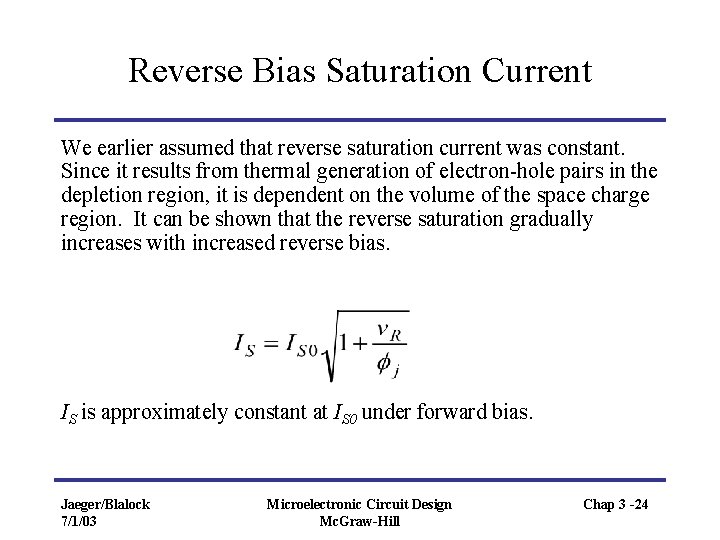
Reverse Bias Saturation Current We earlier assumed that reverse saturation current was constant. Since it results from thermal generation of electron-hole pairs in the depletion region, it is dependent on the volume of the space charge region. It can be shown that the reverse saturation gradually increases with increased reverse bias. IS is approximately constant at IS 0 under forward bias. Jaeger/Blalock 7/1/03 Microelectronic Circuit Design Mc. Graw-Hill Chap 3 -24

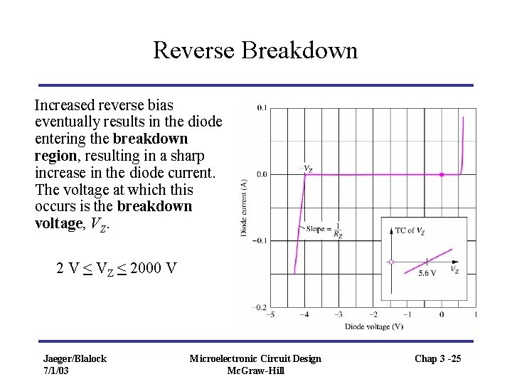
Reverse Breakdown Increased reverse bias eventually results in the diode entering the breakdown region, resulting in a sharp increase in the diode current. The voltage at which this occurs is the breakdown voltage, VZ. 2 V < VZ < 2000 V Jaeger/Blalock 7/1/03 Microelectronic Circuit Design Mc. Graw-Hill Chap 3 -25

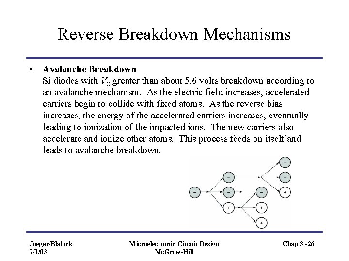
Reverse Breakdown Mechanisms • Avalanche Breakdown Si diodes with VZ greater than about 5. 6 volts breakdown according to an avalanche mechanism. As the electric field increases, accelerated carriers begin to collide with fixed atoms. As the reverse bias increases, the energy of the accelerated carriers increases, eventually leading to ionization of the impacted ions. The new carriers also accelerate and ionize other atoms. This process feeds on itself and leads to avalanche breakdown. Jaeger/Blalock 7/1/03 Microelectronic Circuit Design Mc. Graw-Hill Chap 3 -26

Reverse Breakdown Mechanisms (cont. ) • Zener Breakdown Zener breakdown occurs in heavily doped diodes. The heavy doping results in a very narrow depletion region at the diode junction. Reverse bias leads to carriers with sufficient energy to tunnel directly between conduction and valence bands moving across the junction. Once the tunneling threshold is reached, additional reverse bias leads to a rapidly increasing reverse current. • Breakdown Voltage Temperature Coefficient Temperature coefficient is a quick way to distinguish breakdown mechanisms. Avalanche breakdown voltage increases with temperature, zener breakdown decreases with temperature. For silicon diodes, zero temperature coefficient is achieved at approximately 5. 6 V. Jaeger/Blalock 7/1/03 Microelectronic Circuit Design Mc. Graw-Hill Chap 3 -27

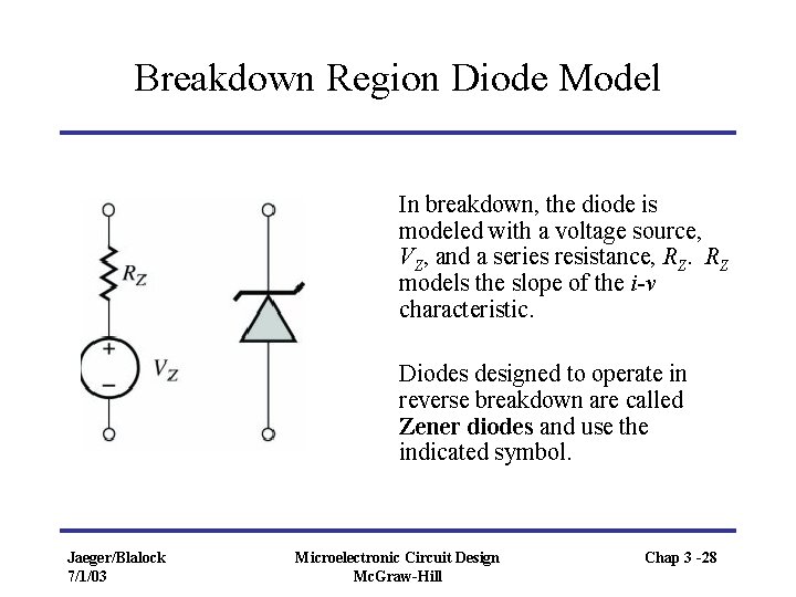
Breakdown Region Diode Model In breakdown, the diode is modeled with a voltage source, VZ, and a series resistance, RZ. RZ models the slope of the i-v characteristic. Diodes designed to operate in reverse breakdown are called Zener diodes and use the indicated symbol. Jaeger/Blalock 7/1/03 Microelectronic Circuit Design Mc. Graw-Hill Chap 3 -28

PN Junction Capacitance • The capacitance is important under dynamic signal conditions because it prevents the voltage across the diode from changing instantaneously. Jaeger/Blalock 7/1/03 Microelectronic Circuit Design Mc. Graw-Hill

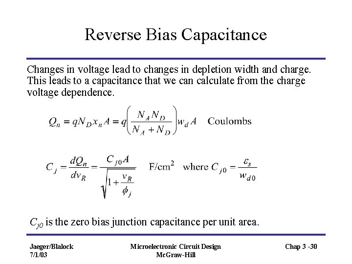
Reverse Bias Capacitance Changes in voltage lead to changes in depletion width and charge. This leads to a capacitance that we can calculate from the charge voltage dependence. Cj 0 is the zero bias junction capacitance per unit area. Jaeger/Blalock 7/1/03 Microelectronic Circuit Design Mc. Graw-Hill Chap 3 -30

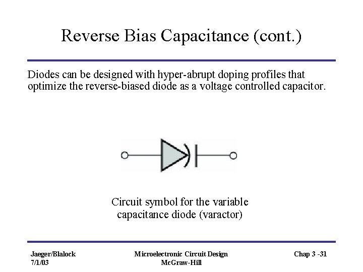
Reverse Bias Capacitance (cont. ) Diodes can be designed with hyper-abrupt doping profiles that optimize the reverse-biased diode as a voltage controlled capacitor. Circuit symbol for the variable capacitance diode (varactor) Jaeger/Blalock 7/1/03 Microelectronic Circuit Design Mc. Graw-Hill Chap 3 -31

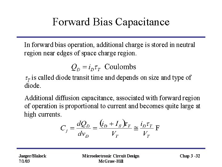
Forward Bias Capacitance In forward bias operation, additional charge is stored in neutral region near edges of space charge region. t. T is called diode transit time and depends on size and type of diode. Additional diffusion capacitance, associated with forward region of operation is proportional to current and becomes quite large at high currents. Jaeger/Blalock 7/1/03 Microelectronic Circuit Design Mc. Graw-Hill Chap 3 -32

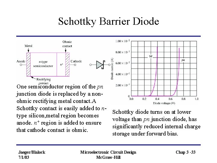
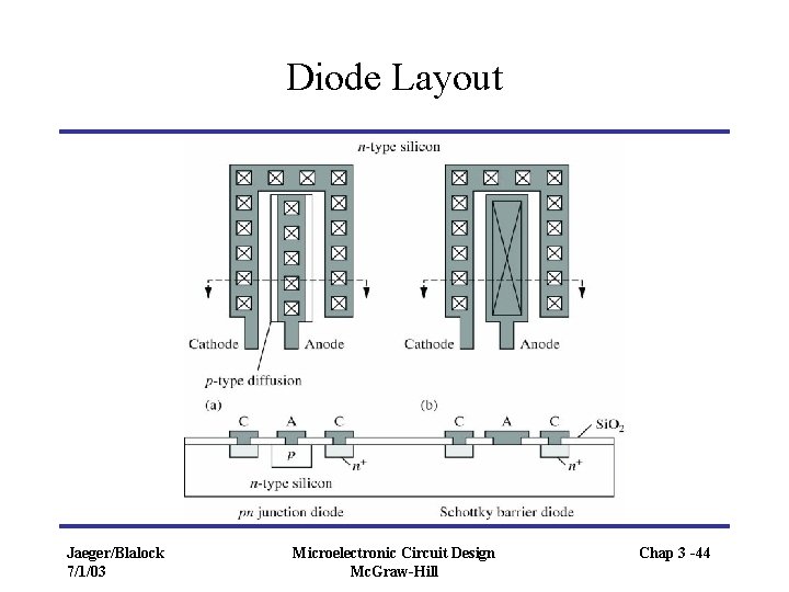
Schottky Barrier Diode One semiconductor region of the pn junction diode is replaced by a nonohmic rectifying metal contact. A Schottky contact is easily added to n. Schottky diode turns on at lower type silicon, metal region becomes voltage than pn junction diode, has anode. n+ region is added to ensure significantly reduced internal charge that cathode contact is ohmic. storage under forward bias. Jaeger/Blalock 7/1/03 Microelectronic Circuit Design Mc. Graw-Hill Chap 3 -33

Schottky Diode • Key uniqueness: fast switching from ON to OFF and back. • Widely used: – in analog circuits: in track and hold circuits in A/D converters, pin drivers of IC test equipment – in communications and radar applications: as detectors and mixers, also as varactors Jaeger/Blalock 7/1/03 Microelectronic Circuit Design Mc. Graw-Hill

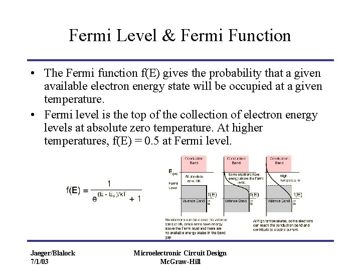
Fermi Level & Fermi Function • The Fermi function f(E) gives the probability that a given available electron energy state will be occupied at a given temperature. • Fermi level is the top of the collection of electron energy levels at absolute zero temperature. At higher temperatures, f(E) = 0. 5 at Fermi level. Jaeger/Blalock 7/1/03 Microelectronic Circuit Design Mc. Graw-Hill

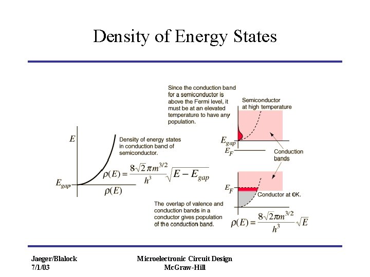
Density of Energy States Jaeger/Blalock 7/1/03 Microelectronic Circuit Design Mc. Graw-Hill

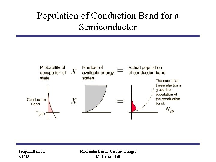
Population of Conduction Band for a Semiconductor Jaeger/Blalock 7/1/03 Microelectronic Circuit Design Mc. Graw-Hill

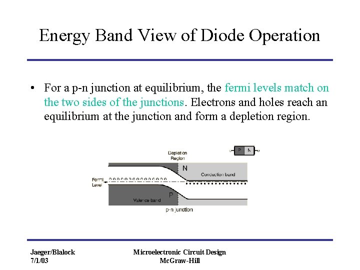
Energy Band View of Diode Operation • For a p-n junction at equilibrium, the fermi levels match on the two sides of the junctions. Electrons and holes reach an equilibrium at the junction and form a depletion region. Jaeger/Blalock 7/1/03 Microelectronic Circuit Design Mc. Graw-Hill

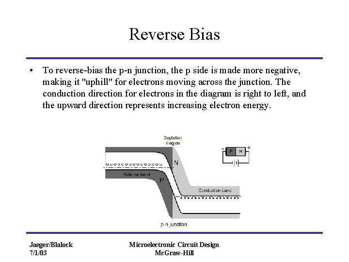
Reverse Bias • To reverse-bias the p-n junction, the p side is made more negative, making it "uphill" for electrons moving across the junction. The conduction direction for electrons in the diagram is right to left, and the upward direction represents increasing electron energy. Jaeger/Blalock 7/1/03 Microelectronic Circuit Design Mc. Graw-Hill

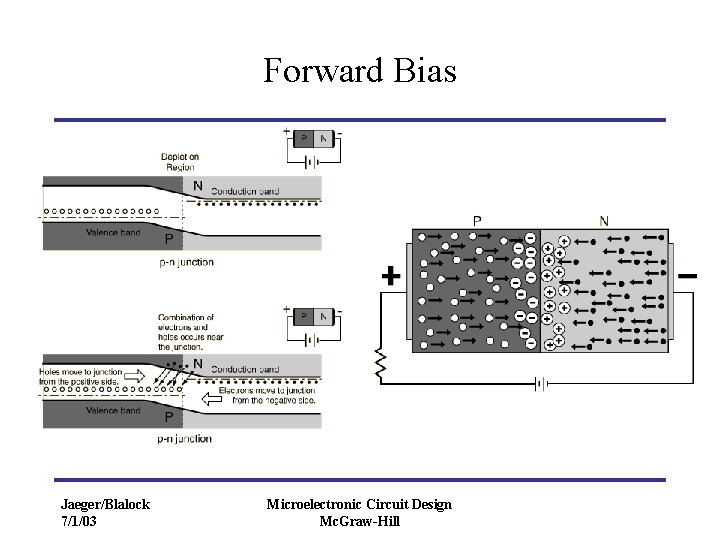
Forward Bias Jaeger/Blalock 7/1/03 Microelectronic Circuit Design Mc. Graw-Hill

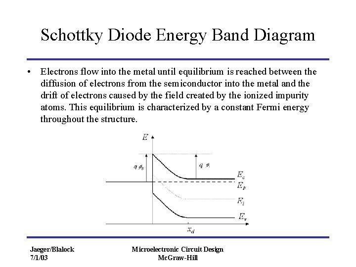
Schottky Diode Energy Band Diagram • Electrons flow into the metal until equilibrium is reached between the diffusion of electrons from the semiconductor into the metal and the drift of electrons caused by the field created by the ionized impurity atoms. This equilibrium is characterized by a constant Fermi energy throughout the structure. Jaeger/Blalock 7/1/03 Microelectronic Circuit Design Mc. Graw-Hill

Ohmic Contact • a contact between a metal and a semiconductor is typically a Schottky barrier contact. • However, if the semiconductor is very highly doped, the Schottky barrier depletion region becomes very thin. At very high doping levels, a thin depletion layer becomes quite transparent for electron tunneling. • a practical way to make a good ohmic contact is to make a very highly doped semiconductor region between the contact metal and the semiconductor. Jaeger/Blalock 7/1/03 Microelectronic Circuit Design Mc. Graw-Hill

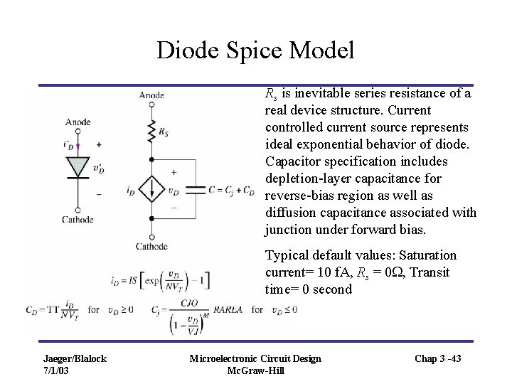
Diode Spice Model Rs is inevitable series resistance of a real device structure. Current controlled current source represents ideal exponential behavior of diode. Capacitor specification includes depletion-layer capacitance for reverse-bias region as well as diffusion capacitance associated with junction under forward bias. Typical default values: Saturation current= 10 f. A, Rs = 0 , Transit time= 0 second Jaeger/Blalock 7/1/03 Microelectronic Circuit Design Mc. Graw-Hill Chap 3 -43

Diode Layout Jaeger/Blalock 7/1/03 Microelectronic Circuit Design Mc. Graw-Hill Chap 3 -44

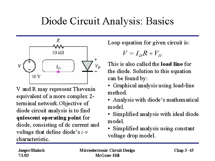
Diode Circuit Analysis: Basics Loop equation for given circuit is: V and R may represent Thevenin equivalent of a more complex 2 terminal network. Objective of diode circuit analysis is to find quiescent operating point for diode, consisting of dc current and voltage that define diode’s i-v characteristic. Jaeger/Blalock 7/1/03 This is also called the load line for the diode. Solution to this equation can be found by: • Graphical analysis using load-line method. • Analysis with diode’s mathematical model. • Simplified analysis with ideal diode model. • Simplified analysis using constant voltage drop model. Microelectronic Circuit Design Mc. Graw-Hill Chap 3 -45

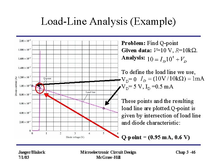
Load-Line Analysis (Example) Problem: Find Q-point Given data: V=10 V, R=10 k. Analysis: To define the load line we use, VD= 0 VD= 5 V, ID =0. 5 m. A These points and the resulting load line are plotted. Q-point is given by intersection of load line and diode characteristic: Q-point = (0. 95 m. A, 0. 6 V) Jaeger/Blalock 7/1/03 Microelectronic Circuit Design Mc. Graw-Hill Chap 3 -46

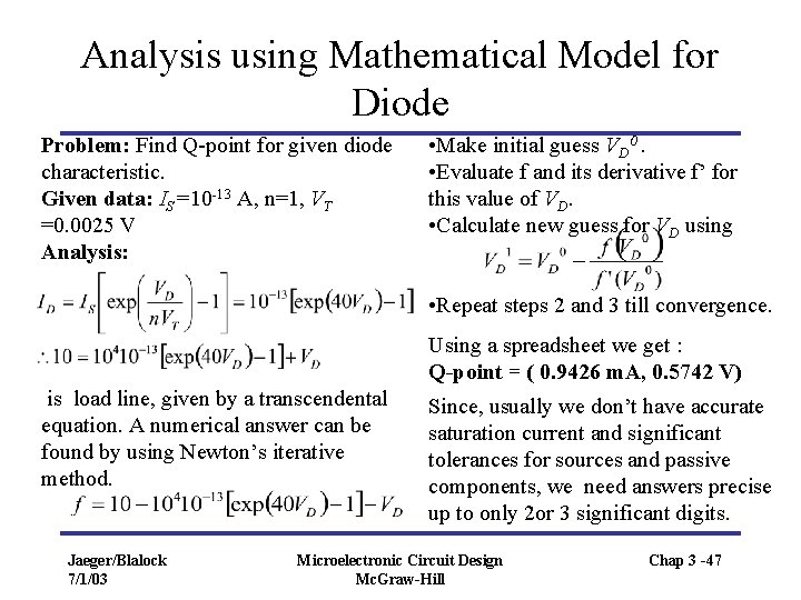
Analysis using Mathematical Model for Diode Problem: Find Q-point for given diode characteristic. Given data: IS =10 -13 A, n=1, VT =0. 0025 V Analysis: • Make initial guess VD 0. • Evaluate f and its derivative f’ for this value of VD. • Calculate new guess for VD using • Repeat steps 2 and 3 till convergence. Using a spreadsheet we get : Q-point = ( 0. 9426 m. A, 0. 5742 V) is load line, given by a transcendental equation. A numerical answer can be found by using Newton’s iterative method. Jaeger/Blalock 7/1/03 Since, usually we don’t have accurate saturation current and significant tolerances for sources and passive components, we need answers precise up to only 2 or 3 significant digits. Microelectronic Circuit Design Mc. Graw-Hill Chap 3 -47

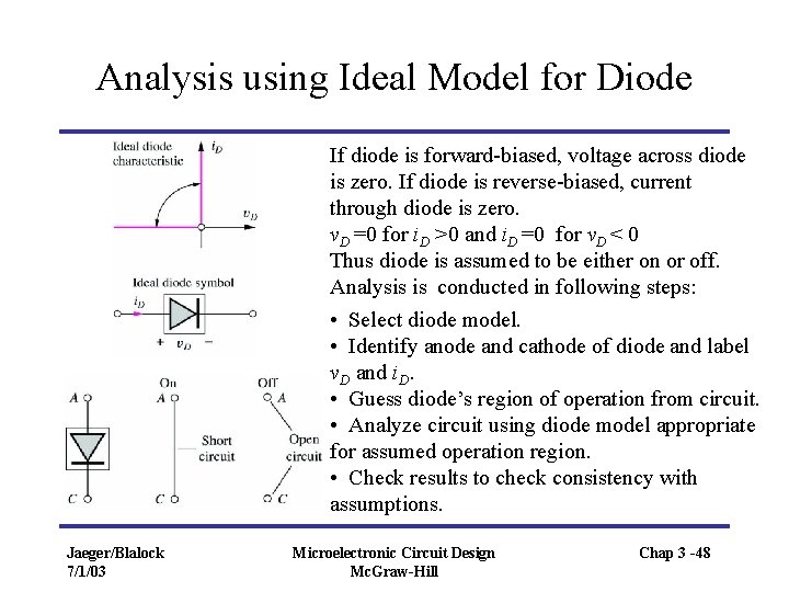
Analysis using Ideal Model for Diode If diode is forward-biased, voltage across diode is zero. If diode is reverse-biased, current through diode is zero. v. D =0 for i. D >0 and i. D =0 for v. D < 0 Thus diode is assumed to be either on or off. Analysis is conducted in following steps: • Select diode model. • Identify anode and cathode of diode and label v. D and i. D. • Guess diode’s region of operation from circuit. • Analyze circuit using diode model appropriate for assumed operation region. • Check results to check consistency with assumptions. Jaeger/Blalock 7/1/03 Microelectronic Circuit Design Mc. Graw-Hill Chap 3 -48

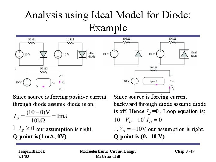
Analysis using Ideal Model for Diode: Example Since source is forcing positive current Since source is forcing current through diode assume diode is on. backward through diode assume diode is off. Hence ID =0. Loop equation is: our assumption is right. Q-point is(1 m. A, 0 V) Jaeger/Blalock 7/1/03 our assumption is right. Q-point is (0, -10 V) Microelectronic Circuit Design Mc. Graw-Hill Chap 3 -49

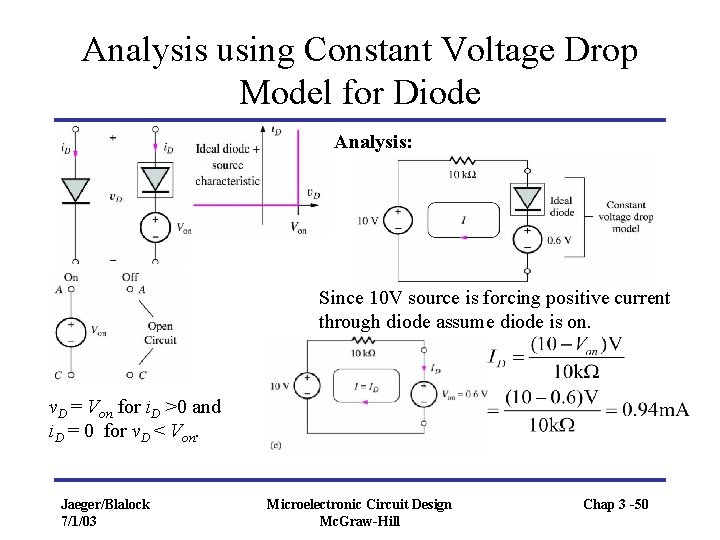
Analysis using Constant Voltage Drop Model for Diode Analysis: Since 10 V source is forcing positive current through diode assume diode is on. v. D = Von for i. D >0 and i. D = 0 for v. D < Von. Jaeger/Blalock 7/1/03 Microelectronic Circuit Design Mc. Graw-Hill Chap 3 -50

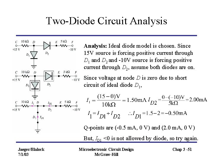
Two-Diode Circuit Analysis: Ideal diode model is chosen. Since 15 V source is forcing positive current through D 1 and D 2 and -10 V source is forcing positive current through D 2, assume both diodes are on. Since voltage at node D is zero due to short circuit of ideal diode D 1, Q-points are (-0. 5 m. A, 0 V) and (2. 0 m. A, 0 V) But, ID 1 <0 is not allowed by diode, so try again. Jaeger/Blalock 7/1/03 Microelectronic Circuit Design Mc. Graw-Hill Chap 3 -51

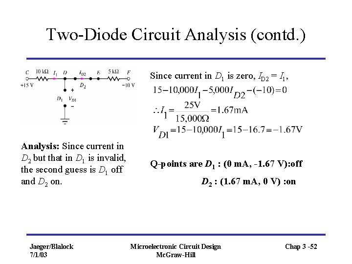
Two-Diode Circuit Analysis (contd. ) Since current in D 1 is zero, ID 2 = I 1, Analysis: Since current in D 2 but that in D 1 is invalid, the second guess is D 1 off and D 2 on. Jaeger/Blalock 7/1/03 Q-points are D 1 : (0 m. A, -1. 67 V): off D 2 : (1. 67 m. A, 0 V) : on Microelectronic Circuit Design Mc. Graw-Hill Chap 3 -52

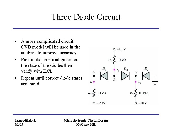
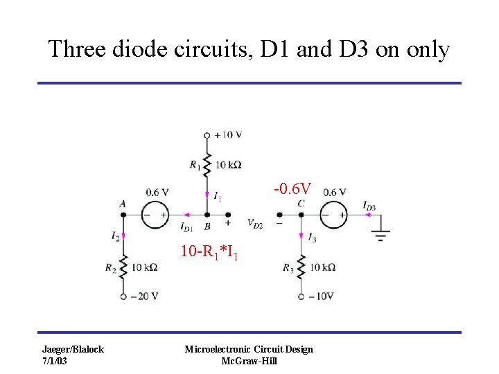
Three Diode Circuit • A more complicated circuit. CVD model will be used in the analysis to improve accuracy. • First make an initial guess on the state of the diodes then verify with KCL • Repeat until correct diode states are found Jaeger/Blalock 7/1/03 Microelectronic Circuit Design Mc. Graw-Hill

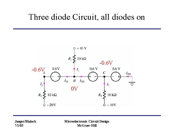
Three diode Circuit, all diodes on -0. 6 V 0 V Jaeger/Blalock 7/1/03 Microelectronic Circuit Design Mc. Graw-Hill

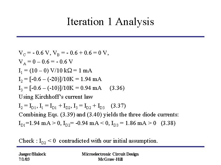
Iteration 1 Analysis VC = - 0. 6 V, VB = - 0. 6 + 0. 6 = 0 V, VA = 0 – 0. 6 = - 0. 6 V I 1 = (10 – 0) V/10 k = 1 m. A I 2 = [-0. 6 – (-20)]/10 K = 1. 94 m. A I 3 = [-0. 6 – (-10)]/10 K = 0. 94 m. A (3. 36) Using Kirchhoff’s current law I 2 = ID 1, I 1 = ID 1 + ID 2, I 3 = ID 2 + ID 3 (3. 37) Combining Eqs. (3. 39) and (3. 40) yields the three diode currents: ID 1=1. 94 m. A > 0, ID 2= -0. 94 m. A < 0, ID 3 = 1. 86 m. A > 0 (3. 38) Check : ID 2 < 0 contradicted with our initial assumption. Jaeger/Blalock 7/1/03 Microelectronic Circuit Design Mc. Graw-Hill

Three diode circuits, D 1 and D 3 on only -0. 6 V 10 -R 1*I 1 Jaeger/Blalock 7/1/03 Microelectronic Circuit Design Mc. Graw-Hill

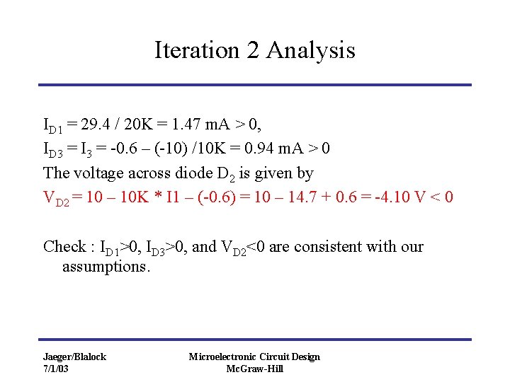
Iteration 2 Analysis ID 1 = 29. 4 / 20 K = 1. 47 m. A > 0, ID 3 = I 3 = -0. 6 – (-10) /10 K = 0. 94 m. A > 0 The voltage across diode D 2 is given by VD 2 = 10 – 10 K * I 1 – (-0. 6) = 10 – 14. 7 + 0. 6 = -4. 10 V < 0 Check : ID 1>0, ID 3>0, and VD 2<0 are consistent with our assumptions. Jaeger/Blalock 7/1/03 Microelectronic Circuit Design Mc. Graw-Hill

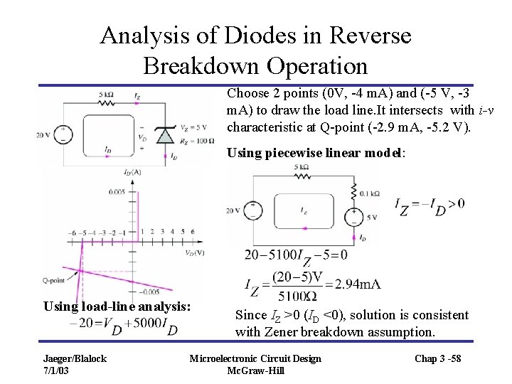
Analysis of Diodes in Reverse Breakdown Operation Choose 2 points (0 V, -4 m. A) and (-5 V, -3 m. A) to draw the load line. It intersects with i-v characteristic at Q-point (-2. 9 m. A, -5. 2 V). Using piecewise linear model: Using load-line analysis: Jaeger/Blalock 7/1/03 Since IZ >0 (ID <0), solution is consistent with Zener breakdown assumption. Microelectronic Circuit Design Mc. Graw-Hill Chap 3 -58

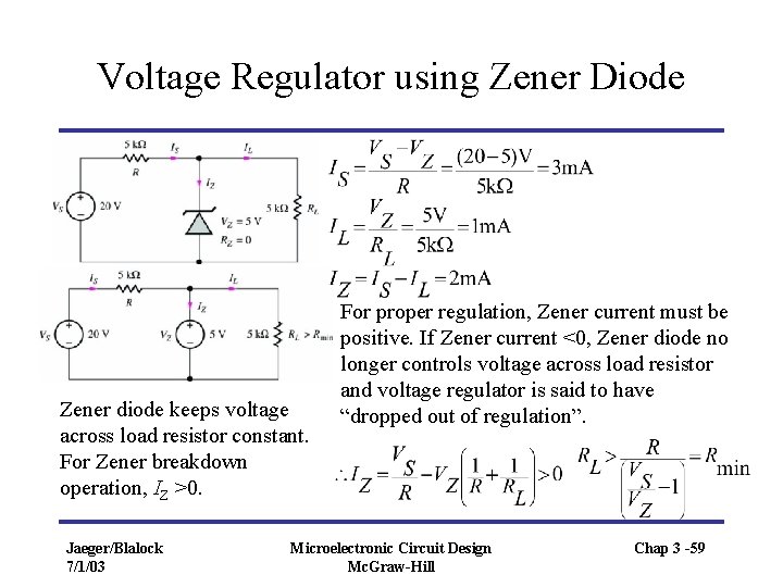
Voltage Regulator using Zener Diode Zener diode keeps voltage across load resistor constant. For Zener breakdown operation, IZ >0. Jaeger/Blalock 7/1/03 For proper regulation, Zener current must be positive. If Zener current <0, Zener diode no longer controls voltage across load resistor and voltage regulator is said to have “dropped out of regulation”. Microelectronic Circuit Design Mc. Graw-Hill Chap 3 -59

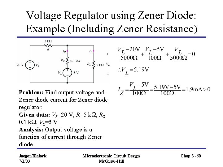
Voltage Regulator using Zener Diode: Example (Including Zener Resistance) Problem: Find output voltage and Zener diode current for Zener diode regulator. Given data: VS=20 V, R=5 k , RZ= 0. 1 k , VZ=5 V Analysis: Output voltage is a function of current through Zener diode. Jaeger/Blalock 7/1/03 Microelectronic Circuit Design Mc. Graw-Hill Chap 3 -60

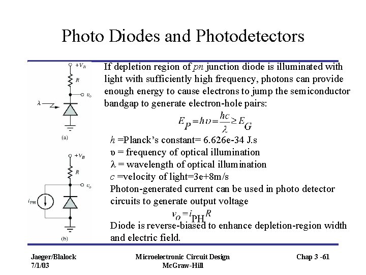
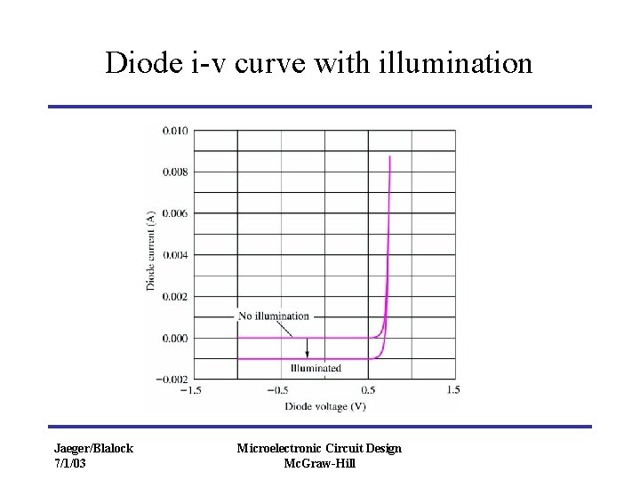
Photo Diodes and Photodetectors If depletion region of pn junction diode is illuminated with light with sufficiently high frequency, photons can provide enough energy to cause electrons to jump the semiconductor bandgap to generate electron-hole pairs: h =Planck’s constant= 6. 626 e-34 J. s υ = frequency of optical illumination l = wavelength of optical illumination c =velocity of light=3 e+8 m/s Photon-generated current can be used in photo detector circuits to generate output voltage Diode is reverse-biased to enhance depletion-region width and electric field. Jaeger/Blalock 7/1/03 Microelectronic Circuit Design Mc. Graw-Hill Chap 3 -61

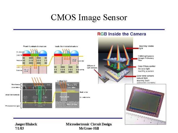
CMOS Image Sensor Jaeger/Blalock 7/1/03 Microelectronic Circuit Design Mc. Graw-Hill

Diode i-v curve with illumination Jaeger/Blalock 7/1/03 Microelectronic Circuit Design Mc. Graw-Hill

Optical Fiber Application • In optical fiber communication systems, the amplitude of the incident light is modulated by rapidly changing digital data, and i. PH is a time-varying signal. The time-varying signal voltage at vo is fed to additional electronic circuits to demodulate the signal and recover the original data that were transmitted down the optical fiber. Jaeger/Blalock 7/1/03 Microelectronic Circuit Design Mc. Graw-Hill

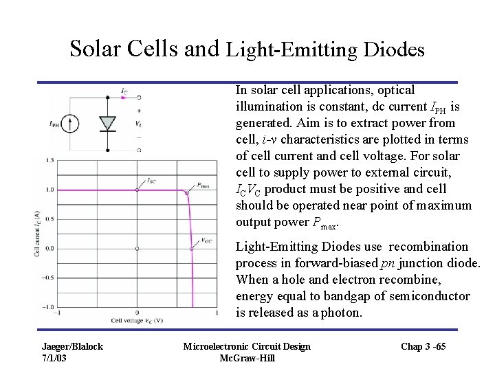
Solar Cells and Light-Emitting Diodes In solar cell applications, optical illumination is constant, dc current IPH is generated. Aim is to extract power from cell, i-v characteristics are plotted in terms of cell current and cell voltage. For solar cell to supply power to external circuit, ICVC product must be positive and cell should be operated near point of maximum output power Pmax. Light-Emitting Diodes use recombination process in forward-biased pn junction diode. When a hole and electron recombine, energy equal to bandgap of semiconductor is released as a photon. Jaeger/Blalock 7/1/03 Microelectronic Circuit Design Mc. Graw-Hill Chap 3 -65

Solar Cell Videos • Next generation cheap solar cell – link • NASA Helios – link • 2008 Solar Challenge - link Jaeger/Blalock 7/1/03 Microelectronic Circuit Design Mc. Graw-Hill

Solar Power for the Home Jaeger/Blalock 7/1/03 Microelectronic Circuit Design Mc. Graw-Hill

LED • Organic LED introduction – link • Sony OLED TV XEL 1 – link • Cool LED light ad - link Jaeger/Blalock 7/1/03 Microelectronic Circuit Design Mc. Graw-Hill

Rectifier Circuits • Basic rectifier converts an ac voltage to a pulsating dc voltage. • A filter then eliminates ac components of the waveform to produce a nearly constant dc voltage output. • Rectifier circuits are used in virtually all electronic devices to convert the 120 V-60 Hz ac power line source to the dc voltages required for operation of the electronic device. • In rectifier circuits, the diode state changes with time and a given piecewise linear model is valid only for a certain time interval. Jaeger/Blalock 7/1/03 Microelectronic Circuit Design Mc. Graw-Hill Chap 3 -69

Delta Electronics • 台達電子集團 (The Delta Group) holds the world's number one position in switching power supplies. • Power Product: – Switching Power Supply – DC / DC converter – Uninterrupted Power Supply (UPS) – AC / DC adapter – Telecom Power Jaeger/Blalock 7/1/03 Microelectronic Circuit Design Mc. Graw-Hill

Delta Electronics

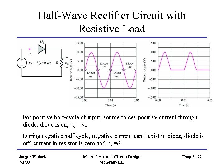
Half-Wave Rectifier Circuit with Resistive Load For positive half-cycle of input, source forces positive current through diode, diode is on, vo = vs. During negative half cycle, negative current can’t exist in diode, diode is off, current in resistor is zero and vo =0. Jaeger/Blalock 7/1/03 Microelectronic Circuit Design Mc. Graw-Hill Chap 3 -72

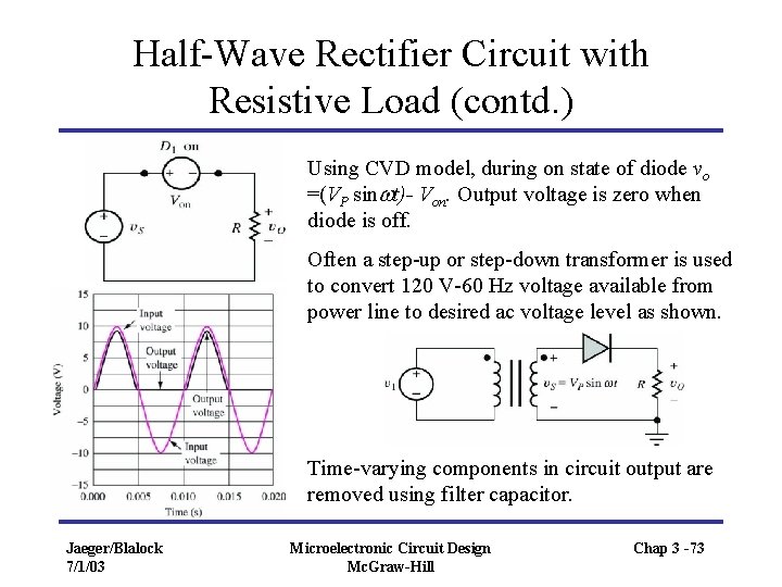
Half-Wave Rectifier Circuit with Resistive Load (contd. ) Using CVD model, during on state of diode vo =(VP sinwt)- Von. Output voltage is zero when diode is off. Often a step-up or step-down transformer is used to convert 120 V-60 Hz voltage available from power line to desired ac voltage level as shown. Time-varying components in circuit output are removed using filter capacitor. Jaeger/Blalock 7/1/03 Microelectronic Circuit Design Mc. Graw-Hill Chap 3 -73

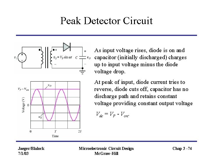
Peak Detector Circuit As input voltage rises, diode is on and capacitor (initially discharged) charges up to input voltage minus the diode voltage drop. At peak of input, diode current tries to reverse, diode cuts off, capacitor has no discharge path and retains constant voltage providing constant output voltage Vdc = VP - Von. Jaeger/Blalock 7/1/03 Microelectronic Circuit Design Mc. Graw-Hill Chap 3 -74

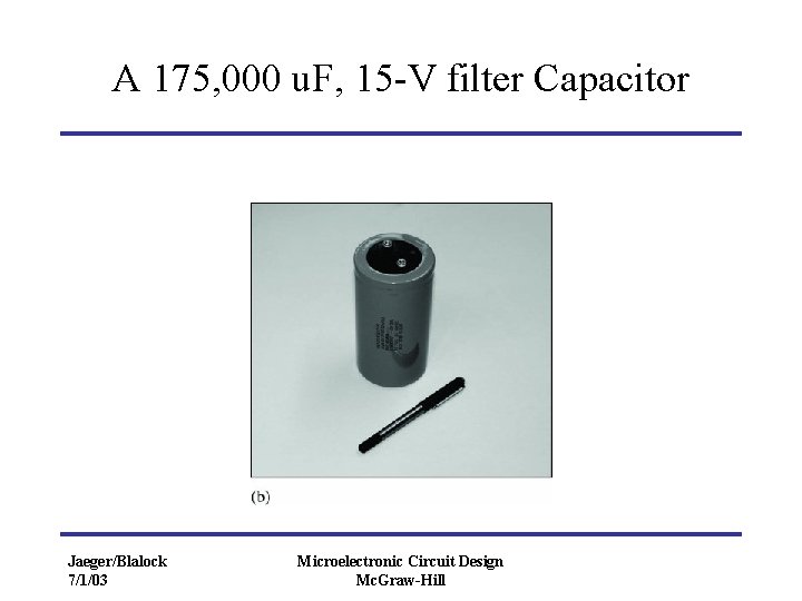
A 175, 000 u. F, 15 -V filter Capacitor Jaeger/Blalock 7/1/03 Microelectronic Circuit Design Mc. Graw-Hill

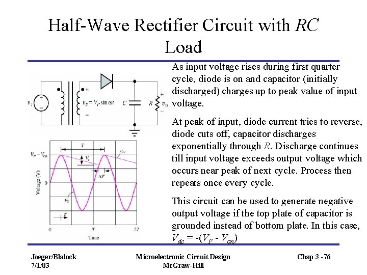
Half-Wave Rectifier Circuit with RC Load As input voltage rises during first quarter cycle, diode is on and capacitor (initially discharged) charges up to peak value of input voltage. At peak of input, diode current tries to reverse, diode cuts off, capacitor discharges exponentially through R. Discharge continues till input voltage exceeds output voltage which occurs near peak of next cycle. Process then repeats once every cycle. This circuit can be used to generate negative output voltage if the top plate of capacitor is grounded instead of bottom plate. In this case, Vdc = -(VP - Von) Jaeger/Blalock 7/1/03 Microelectronic Circuit Design Mc. Graw-Hill Chap 3 -76

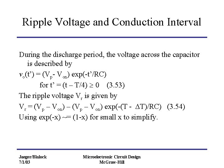
Ripple Voltage and Conduction Interval During the discharge period, the voltage across the capacitor is described by vo(t’) = (Vp- Von) exp(-t’/RC) for t’ = (t – T/4) 0 (3. 53) The ripple voltage Vr is given by Vr = (Vp – Von) – (Vp – Von) exp(-(T - T)/RC) (3. 54) Using exp(-x) ~= (1 -x) for small x to simplify. Jaeger/Blalock 7/1/03 Microelectronic Circuit Design Mc. Graw-Hill

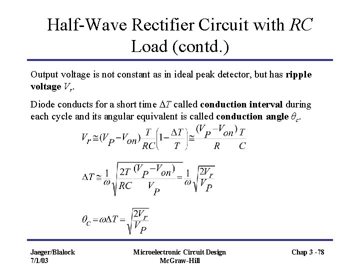
Half-Wave Rectifier Circuit with RC Load (contd. ) Output voltage is not constant as in ideal peak detector, but has ripple voltage Vr. Diode conducts for a short time T called conduction interval during each cycle and its angular equivalent is called conduction angle θc. Jaeger/Blalock 7/1/03 Microelectronic Circuit Design Mc. Graw-Hill Chap 3 -78

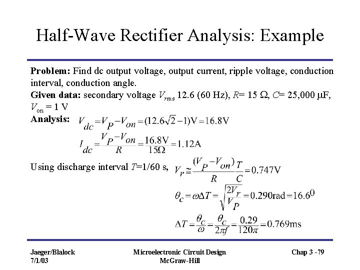
Half-Wave Rectifier Analysis: Example Problem: Find dc output voltage, output current, ripple voltage, conduction interval, conduction angle. Given data: secondary voltage Vrms 12. 6 (60 Hz), R= 15 , C= 25, 000 m. F, Von = 1 V Analysis: Using discharge interval T=1/60 s, Jaeger/Blalock 7/1/03 Microelectronic Circuit Design Mc. Graw-Hill Chap 3 -79

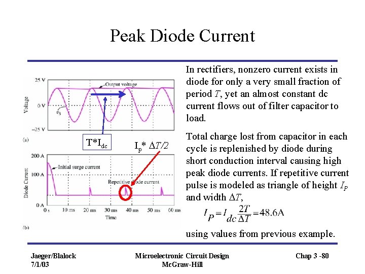
Peak Diode Current In rectifiers, nonzero current exists in diode for only a very small fraction of period T, yet an almost constant dc current flows out of filter capacitor to load. T*Idc Ip* T/2 Total charge lost from capacitor in each cycle is replenished by diode during short conduction interval causing high peak diode currents. If repetitive current pulse is modeled as triangle of height IP and width T, using values from previous example. Jaeger/Blalock 7/1/03 Microelectronic Circuit Design Mc. Graw-Hill Chap 3 -80

Surge Current Besides peak diode currents, when power supply is turned on, there is an even larger current through diode called surge current. During first quarter cycle, current through diode is approximately Peak values of this initial surge current occurs at t = 0+: using values from previous example. Actual values of surge current won’t be as large as predicted because of neglected series resistance associated with rectifier diode as well as transformer. Jaeger/Blalock 7/1/03 Microelectronic Circuit Design Mc. Graw-Hill Chap 3 -81

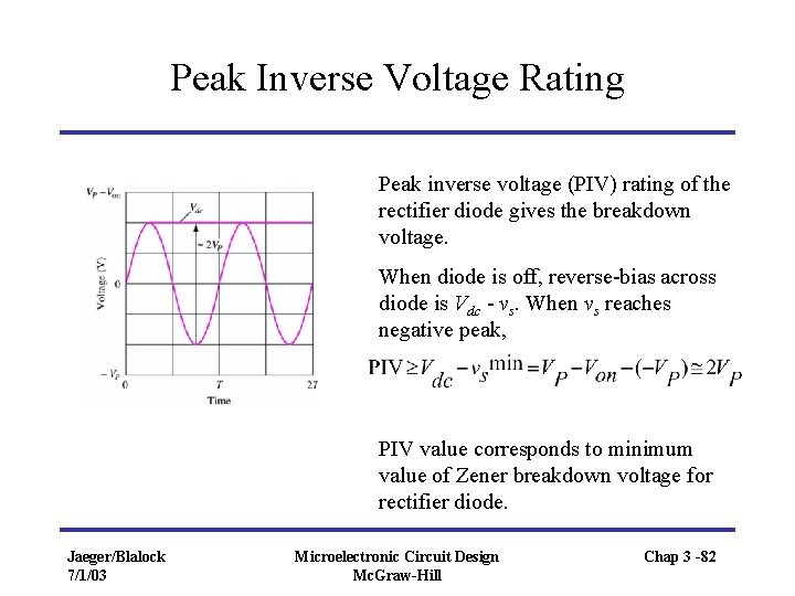
Peak Inverse Voltage Rating Peak inverse voltage (PIV) rating of the rectifier diode gives the breakdown voltage. When diode is off, reverse-bias across diode is Vdc - vs. When vs reaches negative peak, PIV value corresponds to minimum value of Zener breakdown voltage for rectifier diode. Jaeger/Blalock 7/1/03 Microelectronic Circuit Design Mc. Graw-Hill Chap 3 -82

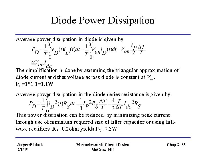
Diode Power Dissipation Average power dissipation in diode is given by The simplification is done by assuming the triangular approximation of diode current and that voltage across diode is constant at Vdc. PD=1*1. 1=1. 1 W Average power dissipation in the diode series resistance is given by This power dissipation can be reduced by minimizing peak current through use of minimum required size of filter capacitor or using fullwave rectifiers. Rs=0. 2 ohm yields PD=7. 3 W Jaeger/Blalock 7/1/03 Microelectronic Circuit Design Mc. Graw-Hill Chap 3 -83

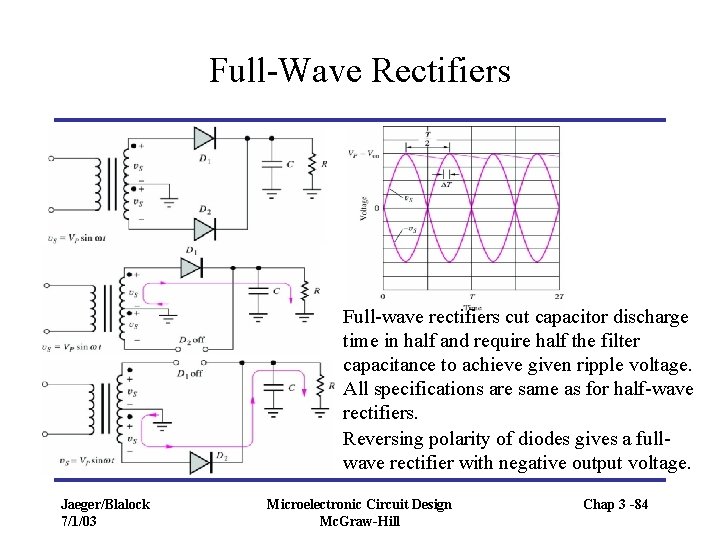
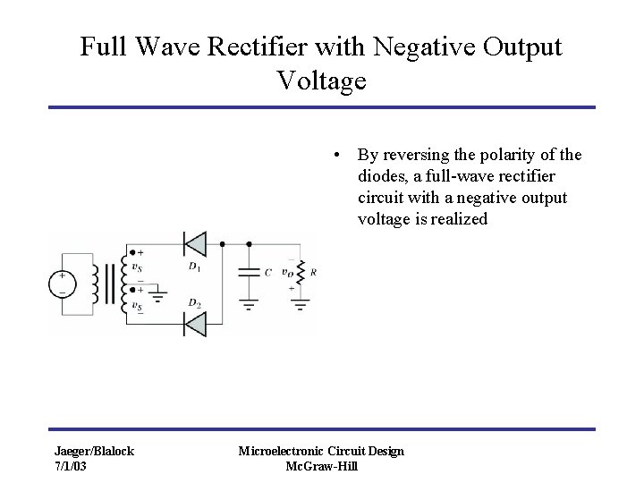
Full-Wave Rectifiers Full-wave rectifiers cut capacitor discharge time in half and require half the filter capacitance to achieve given ripple voltage. All specifications are same as for half-wave rectifiers. Reversing polarity of diodes gives a fullwave rectifier with negative output voltage. Jaeger/Blalock 7/1/03 Microelectronic Circuit Design Mc. Graw-Hill Chap 3 -84

Full Wave vs. Half Wave Rectifier • Same formulas for dc output voltage, ripple voltage, and ΔT, except the discharge interval is T/2 rather than T. • The ripple voltage Vr is halved, the conduction interval ΔT and peak current are reduced. The PIV rating are the same. Jaeger/Blalock 7/1/03 Microelectronic Circuit Design Mc. Graw-Hill

Full Wave Rectifier with Negative Output Voltage • By reversing the polarity of the diodes, a full-wave rectifier circuit with a negative output voltage is realized Jaeger/Blalock 7/1/03 Microelectronic Circuit Design Mc. Graw-Hill

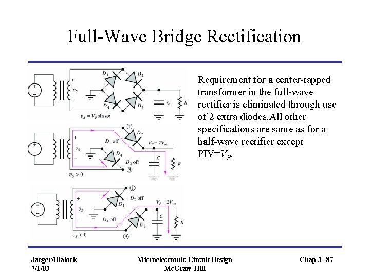
Full-Wave Bridge Rectification Requirement for a center-tapped transformer in the full-wave rectifier is eliminated through use of 2 extra diodes. All other specifications are same as for a half-wave rectifier except PIV=VP. Jaeger/Blalock 7/1/03 Microelectronic Circuit Design Mc. Graw-Hill Chap 3 -87

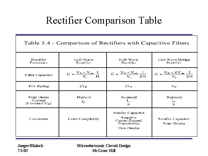
Rectifier Topology Comparison • Filter capacitor is a major factor in determining cost, size and weight in design of rectifiers. • For given ripple voltage, full-wave rectifier requires half the filter capacitance as that in half-wave rectifier. Reduced peak current can reduce heat dissipation in diodes. Benefits of full-wave rectification outweigh increased expenses and circuit complexity (a extra diode and center-tapped transformer). • Bridge rectifier eliminates center-tapped transformer, PIV rating of diodes is reduced. Cost of extra diodes is negligible. Jaeger/Blalock 7/1/03 Microelectronic Circuit Design Mc. Graw-Hill Chap 3 -88

Rectifier Comparison Table Jaeger/Blalock 7/1/03 Microelectronic Circuit Design Mc. Graw-Hill

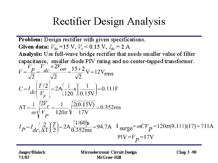
Rectifier Design Analysis Problem: Design rectifier with given specifications. Given data: Vdc =15 V, Vr < 0. 15 V, Idc = 2 A Analysis: Use full-wave bridge rectifier that needs smaller value of filter capacitance, smaller diode PIV rating and no center-tapped transformer. Jaeger/Blalock 7/1/03 Microelectronic Circuit Design Mc. Graw-Hill Chap 3 -90

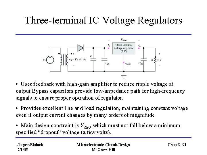
Three-terminal IC Voltage Regulators • Uses feedback with high-gain amplifier to reduce ripple voltage at output. Bypass capacitors provide low-impedance path for high-frequency signals to ensure properation of regulator. • Provides excellent line and load regulation, maintaining constant voltage even if output current changes by many orders of magnitude. • Main design constraint is VREG which must not fall below a minimum specified “dropout” voltage (a few volts). Jaeger/Blalock 7/1/03 Microelectronic Circuit Design Mc. Graw-Hill Chap 3 -91

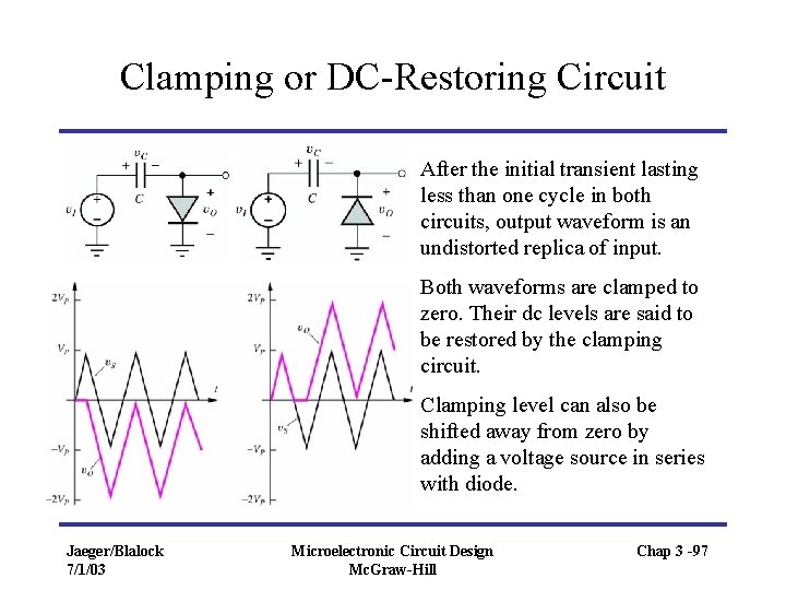
Clamping or DC-Restoring Circuit After the initial transient lasting less than one cycle in both circuits, output waveform is an undistorted replica of input. Both waveforms are clamped to zero. Their dc levels are said to be restored by the clamping circuit. Clamping level can also be shifted away from zero by adding a voltage source in series with diode. Jaeger/Blalock 7/1/03 Microelectronic Circuit Design Mc. Graw-Hill Chap 3 -97

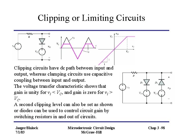
Clipping or Limiting Circuits Clipping circuits have dc path between input and output, whereas clamping circuits use capacitive coupling between input and output. The voltage transfer characteristic shows that gain is unity for v. I < VC, and gain is zero for v. I > VC. A second clipping level can also be set as shown or diodes can be used to control circuit gain by switching resistors in and out of circuits. Jaeger/Blalock 7/1/03 Microelectronic Circuit Design Mc. Graw-Hill Chap 3 -98

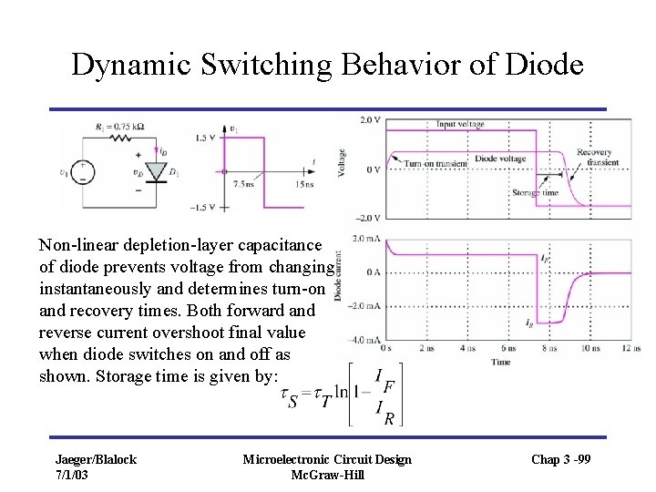
Dynamic Switching Behavior of Diode Non-linear depletion-layer capacitance of diode prevents voltage from changing instantaneously and determines turn-on and recovery times. Both forward and reverse current overshoot final value when diode switches on and off as shown. Storage time is given by: Jaeger/Blalock 7/1/03 Microelectronic Circuit Design Mc. Graw-Hill Chap 3 -99

Homework 3 • Written Homework – 3. 24 – 3. 56 – 3. 69 for figure (b) – 3. 72 for figure (a) – 3. 91 • SPICE Homework for rectifier Jaeger/Blalock 7/1/03 Microelectronic Circuit Design Mc. Graw-Hill