
Unit 1 Diode application and special purpose diodes
- Slides: 51
Unit 1 Diode application and special purpose diodes
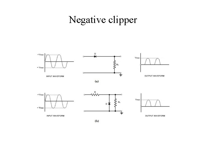
1. 1 Diode clippers • Clipping circuits are wave shaping circuits. • They are useful to clip off the positive or negative portions of an input waveform. • clipper is a device designed to prevent the output of a circuit from exceeding a predetermined voltage level without distorting the remaining part of the applied waveform. • Types of clipper circuit 1. Positive clipper 2. Negative clipper 3. Biased clipper 4. Combination clipper
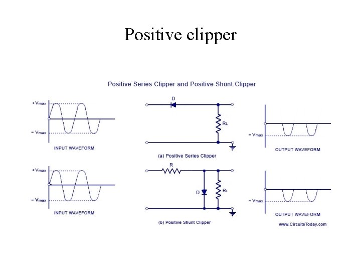
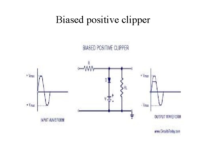
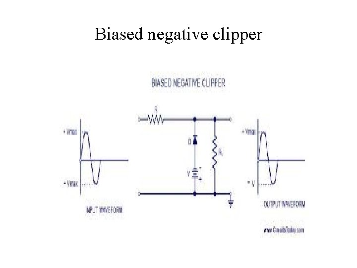
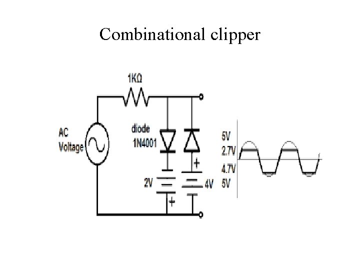
Types of clipper circuits • Positive clipper: it removes the positive half cycles of the input voltage waveform. There are two types of positive clipper (1)series and (2)shunt. • Negative clipper: it removes the negative half cycles of the input voltage waveform. There are two types of negative clipper (1)series and (2)shunt. • Biased clipper : in some application there may be a requirement to remove a small portion of positive or negative half cycle of the signal voltage and hence the biased clipper is used. There are two types (1)biased positive (2)biased negative. • Combination clipper : combination clipper is the combination of biased positive clipper and biased negative clipper.
Positive clipper
Negative clipper
Biased positive clipper
Biased negative clipper
Combinational clipper
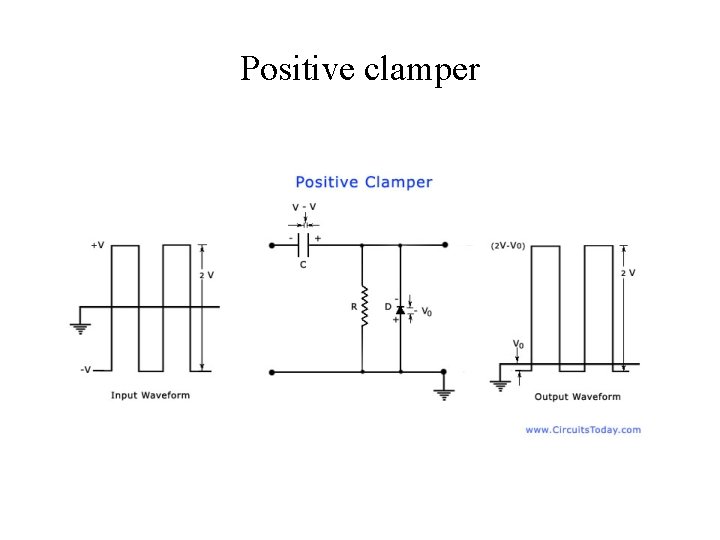
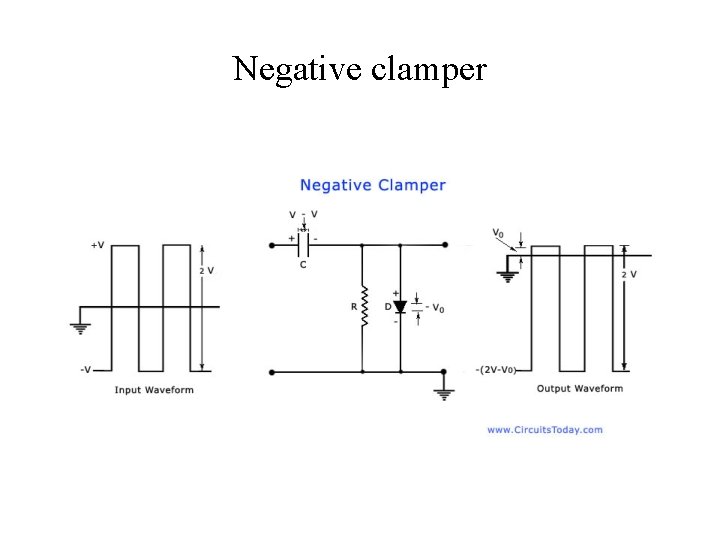
Diode clamper • A clamping circuit is used to place either the positive or negative peak of a signal at a desired level. • The dc component is simply added or subtracted to/from the input signal. • The clamper is also referred to as an IC restorer and ac signal level shifter. • Types of clamper circuit 1. Positive clamper 2. Negative clamper
Positive clamper
Negative clamper
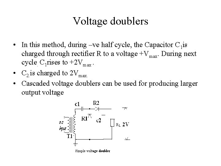
Voltage doublers • In this method, during –ve half cycle, the Capacitor C 1 is charged through rectifier R to a voltage +Vmax. During next cycle. C 1 rises to +2 Vmax. • C 2. is charged to 2 Vmax. • Cascaded voltage doublers can be used for producing larger output voltage
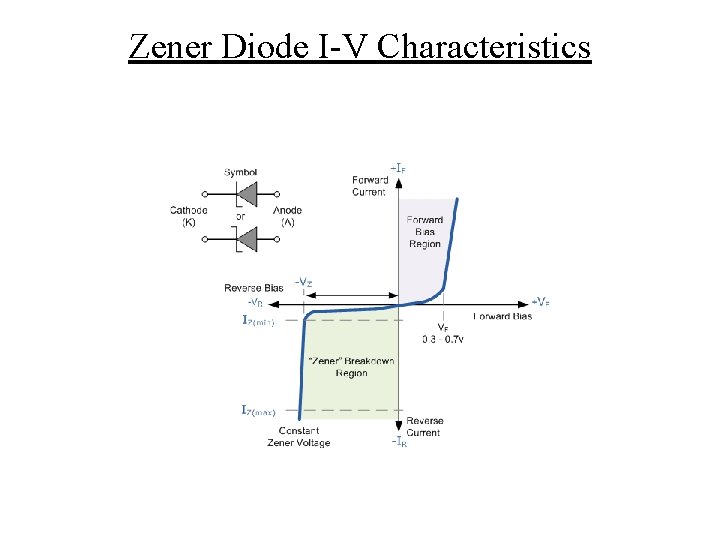
1. 2 Zener diode • A Zener diode is a diode which allows current to flow in the forward direction in the same manner as an ideal diode, but also permits it to flow in the reverse direction when the voltage is above a certain value known as the breakdown voltage, "Zener knee voltage", "Zener voltage", "avalanche point", or "peak inverse voltage". • The device consists of a reverse biased, highly doped, p-n junction diode operating in the breakdown region. • Conventional diodes and rectifiers never operate in the breakdown region, but the Zener diode makes a virtue of it and can safely be operated at this point.
Zener Diode I-V Characteristics
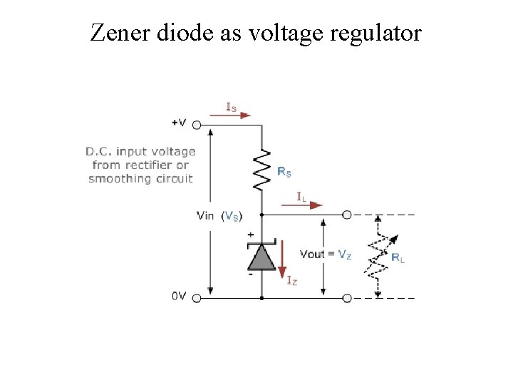
Zener diode as voltage regulator
Zener diode as voltage regulator • The resistor, RS is connected in series with the zener diode to limit the current flow through the diode with the voltage source, VS being connected across the combination. • The stabilized output voltage Vout is taken from across the zener diode. • The zener diode is connected with its cathode terminal connected to the positive rail of the DC supply so it is reverse biased and will be operating in its breakdown condition. • Resistor RS is selected so to limit the maximum current flowing in the circuit • By passing a small current through the diode from a voltage source, via a suitable current limiting resistor (RS), the zener diode will conduct sufficient current to maintain a voltage drop of Vout. .
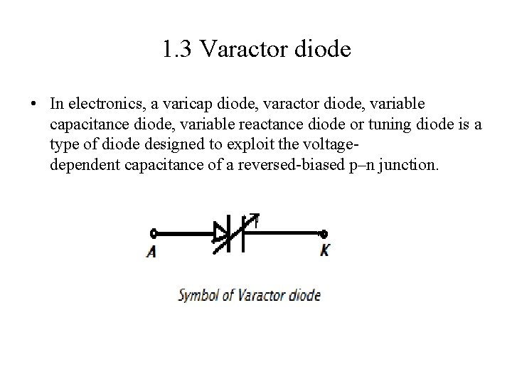
1. 3 Varactor diode • In electronics, a varicap diode, varactor diode, variable capacitance diode, variable reactance diode or tuning diode is a type of diode designed to exploit the voltagedependent capacitance of a reversed-biased p–n junction.
Varactor diode • Varactors are operated in a reverse-biased state. No current flows, but since thickness of the depletion zone varies with the applied bias voltage, the capacitance of the diode can be made to vary. • Generally, the depletion region thickness is proportional to the square root of the applied voltage; capacitance is inversely proportional to the depletion region thickness. Thus, the capacitance is inversely proportional to the square root of applied voltage. • All diodes exhibit this phenomenon to some degree, but varactor diodes are manufactured specifically to exploit this effect and increase the capacitance (and thus the range of variability), whereas most ordinary diode fabrication strives to minimize the capacitance.
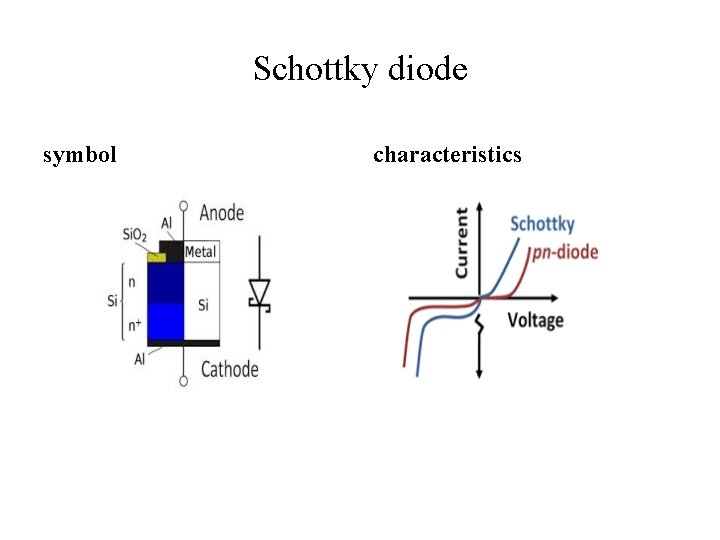
Schottky diode symbol characteristics
Schottky diode • The Schottky diode also known as hot carrier diode, is a semiconductor diode with a low forward voltage drop and a very fast switching action • When forward current flows through a solid-state diode, there is a small voltage drop across its terminals. • A silicon diode has a typical voltage drop of 0. 6– 0. 7 V, while a Schottky diode has a voltage drop of 0. 15– 0. 45 V. • This lower voltage drop can be used to give higher switching speeds and better system efficiency. • A metal–semiconductor junction is formed between a metal and a semiconductor, creating a Schottky barrier • Typical metals used are molybdenum, platinum, chromium or tungsten, and certain silicides (e. g. , palladiu silicide and platinum silicide), whereas the semiconductor would typically be n-type silicon.
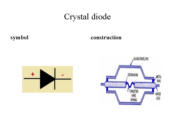
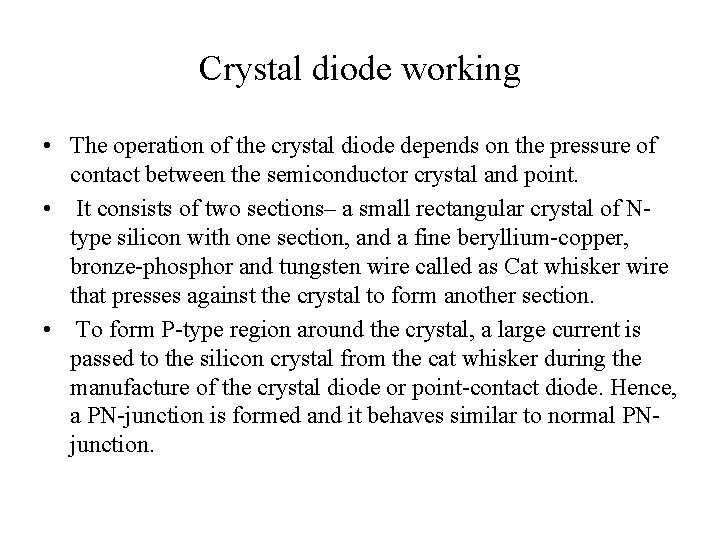
Crystal diode symbol construction
Crystal diode working • The operation of the crystal diode depends on the pressure of contact between the semiconductor crystal and point. • It consists of two sections– a small rectangular crystal of Ntype silicon with one section, and a fine beryllium-copper, bronze-phosphor and tungsten wire called as Cat whisker wire that presses against the crystal to form another section. • To form P-type region around the crystal, a large current is passed to the silicon crystal from the cat whisker during the manufacture of the crystal diode or point-contact diode. Hence, a PN-junction is formed and it behaves similar to normal PNjunction.
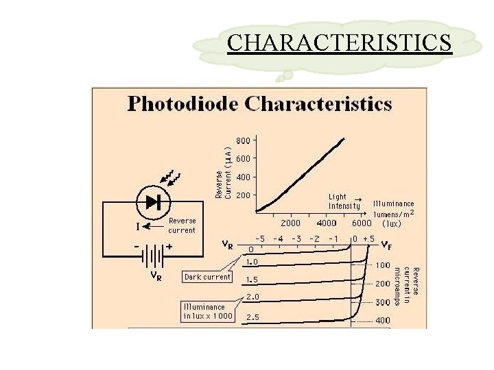
1. 4 PHOTO DIODE A photodiode is a type of photodetector capable of converting light into either current or voltage, depending upon the mode of operation. The common, traditional solar cell used to generate electric solar power is a large area photodiode. OPERATION • A photodiode is designed to operate in reverse bias. • Photoelectric effect. • Photocurrent.
CHARACTERISTICS
APPLICATIONS • P-N photodiodes are used in similar applications to other photo detectors, such as photoconductors, chargecoupled devices, and photomultiplier tubes. They may be used to generate an output which is dependent upon the illumination (analog; for measurement and the like), or to change the state of circuitry (digital; either for control and switching, or digital signal processing). . • Photodiodes are used in consumer electronics devices such as compact disc players, smoke detectors, and the receivers for infrared remote control devices used to control equipment from televisions to air conditioners. For
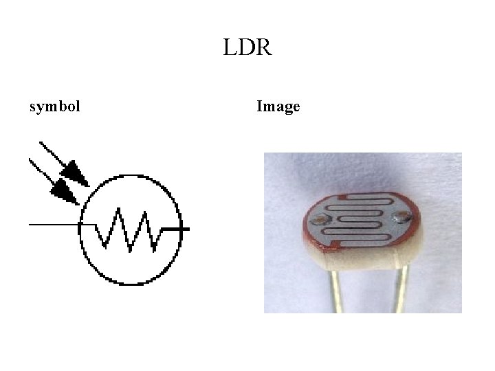
LDR symbol Image
LDR • A photo resistor or light-dependent resistor (LDR) or photocell is a light-controlled variable resistor. • The resistance of a photo resistor decreases with increasing incident light intensity; A photo resistor can be applied in light -sensitive detector circuits, and light- and dark-activated switch • A photo resistor is made of a high resistance semiconductor. In the dark, a photo resistor can have a resistance as high as several megohms (MΩ), while in the light, a photo resistor can have a resistance as low as a few hundred ohms.
Application • Photo resistors come in many types. Inexpensive cadmium sulphide cells can be found in many consumer items such as camera light meters, clock radios, alarm devices (as the detector for a light beam), night lights, outdoor clocks, solar street lamps and solar road studs, etc.
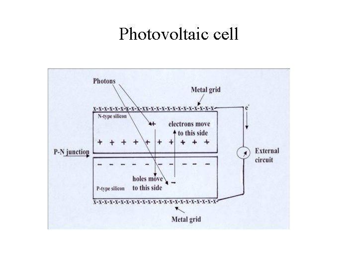
Photovoltaic cell
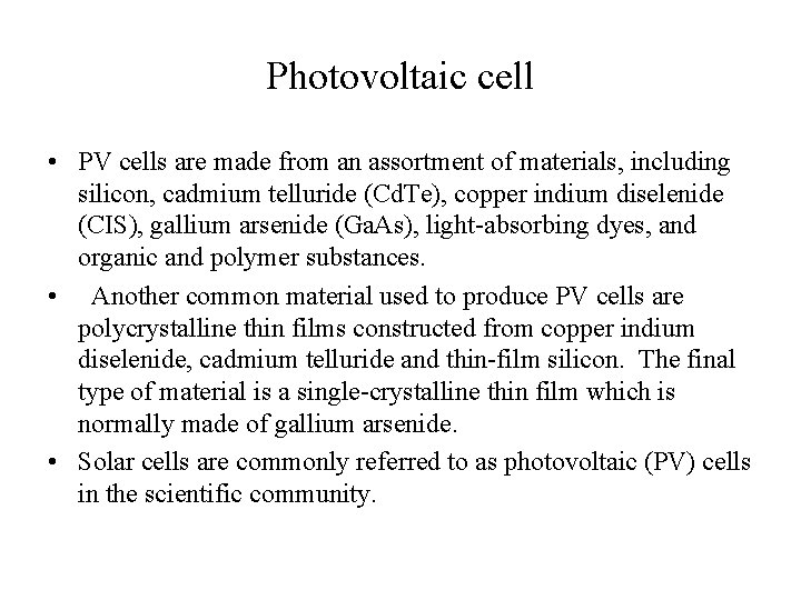
Photovoltaic cell • PV cells are made from an assortment of materials, including silicon, cadmium telluride (Cd. Te), copper indium diselenide (CIS), gallium arsenide (Ga. As), light-absorbing dyes, and organic and polymer substances. • Another common material used to produce PV cells are polycrystalline thin films constructed from copper indium diselenide, cadmium telluride and thin-film silicon. The final type of material is a single-crystalline thin film which is normally made of gallium arsenide. • Solar cells are commonly referred to as photovoltaic (PV) cells in the scientific community.
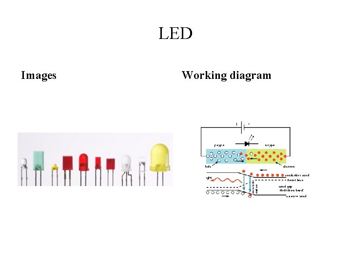
LED • A light-emitting diode (LED) is a two lead light source. • It is a p–n junction diode, which emits light when activated. • When a suitable voltage is applied to the leads, electrons are able to recombine with electron holes within the device, releasing energy in the form of photons. • This effect is called electroluminescence, and the color of the light (corresponding to the energy of the photon) is determined by the energy band gap of the semiconductor.
LED Images Working diagram
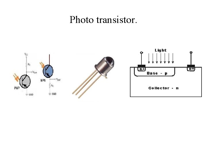
Photo transistor.
Photo transistor • A photo transistor is nothing but an ordinary bi-poplar transistor in which the base region is exposed to the illumination. It is available in both the P-N-P and N-P-N types having different configurations like common emitter, common collector and common base. • Common emitter configuration is generally used. It can also work while base is made open. Compared to the conventional transistor it has more base and collector areas. Ancient photo transistors used single semiconductor materials like silicon and germanium but now a day’s modern components uses materials like gallium and arsenide for high efficiency levels. The base is the lead responsible for activating the transistor. • It is the gate controller device for the larger electrical supply. The collector is the positive lead and the larger electrical supply. The emitter is the negative lead and the outlet for the larger electrical supply.
Features • • Low-cost visible and near-IR photo detection. Available with gains from 100 to over 1500. Moderately fast response times. Available in a wide range of packages including epoxy-coated, transfer-molded and surface mounting technology. • Electrical characteristics similar to that of signal transistors.
Advantages of Photo transistors: • Phototransistors have several important advantages that separate them from other optical sensor some of them are mentioned below • Phototransistors produce a higher current than photo diodes. • Phototransistors are relatively inexpensive, simple, and small enough to fit several of them onto a single integrated computer chip. • Phototransistors are very fast and are capable of providing nearly instantaneous output.
Disadvantages of Photo transistors: • Phototransistors that are made of silicon are not capable of handling voltages over 1, 000 Volts. • Phototransistors are also more vulnerable to surges and spikes of electricity as well as electromagnetic energy. • Phototransistors also do not allow electrons to move as freely as other devices do, such as electron tubes.
Areas of application for the Phototransistor • • • Punch-card readers. Security systems Encoders – measure speed and direction IR detectors photo electric controls Computer logic circuitry. Relays Lighting control (highways etc) Level indication Counting systems
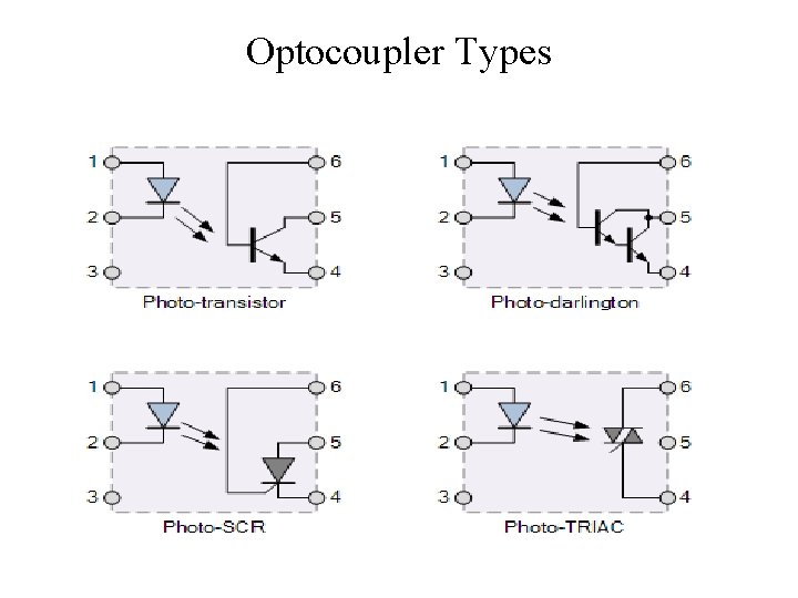
Opto coupler/opto isolator • An Opto coupler, also known as an Opto-isolator or Photocoupler, is an electronic components that interconnects two separate electrical circuits by means of a light sensitive optical interface. • The basic design of an opto coupler consists of an LED that produces infra-red light and a semiconductor photo-sensitive device that is used to detect the emitted infra-red beam. Both the LED and photo-sensitive device are enclosed in a lighttight body or package with metal legs for the electrical connections • An opto coupler or opto-isolator consists of a light emitter, the LED and a light sensitive receiver which can be a single photo -diode, photo-transistor, photo-resistor, photo-SCR, or a photo. TRIAC and the basic operation of an opto coupler is very simple to understand.
Optocoupler Types
Opto coupler Applications • Opt couplers and opto-isolators can be used on their own, or to switch a range of other larger electronic devices such as transistors and triacs providing the required electrical isolation between a lower voltage control signal and the higher voltage or current output signal. • Common applications for optocouplers include microprocessor input/output switching, DC and AC power control, PC communications, signal isolation and power supply regulation which suffer from current ground loops, etc. The electrical signal being transmitted can be either analogue (linear) or digital (pulses).
Seven segment display • A seven-segment display , or seven-segment indicator, is electronic display device for displaying decimal numerals that is an alternative to the more complex dot matrix displays. • Seven-segment displays are widely used in digital clocks, electronic meters, basic calculators, and other electronic devices that display numerical information
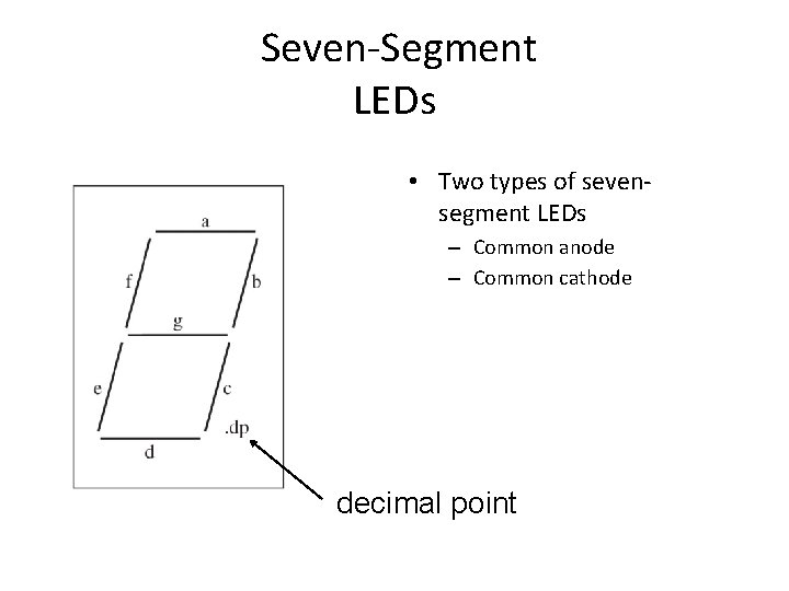
Seven-Segment LEDs • Two types of sevensegment LEDs – Common anode – Common cathode decimal point
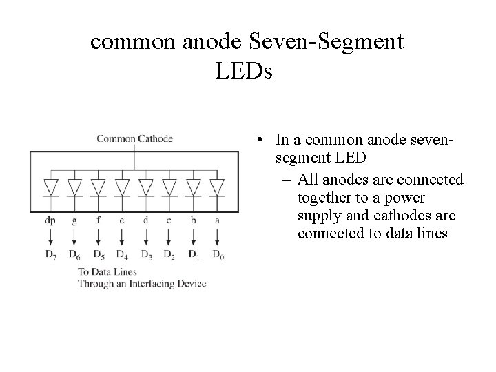
common anode Seven-Segment LEDs • In a common anode sevensegment LED – All anodes are connected together to a power supply and cathodes are connected to data lines
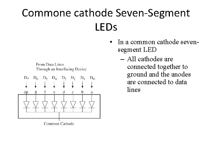
Commone cathode Seven-Segment LEDs • In a common cathode sevensegment LED – All cathodes are connected together to ground and the anodes are connected to data lines
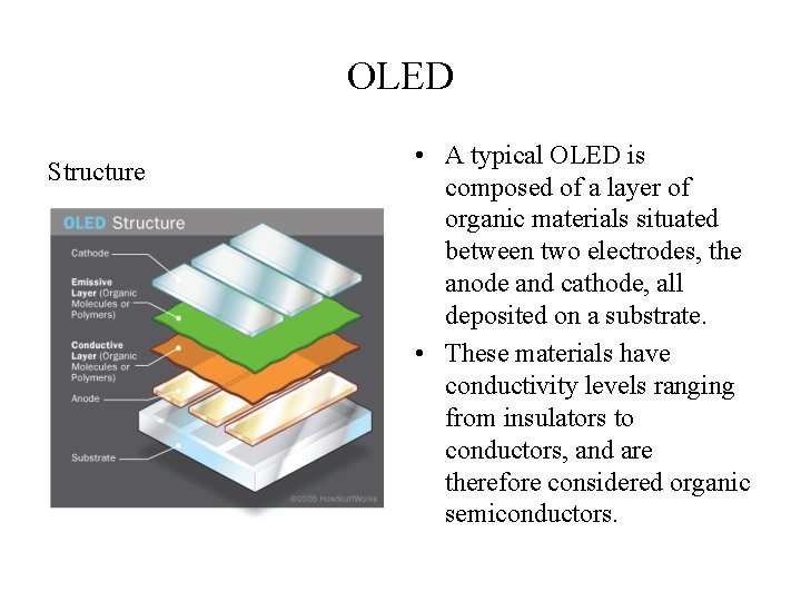
OLED Structure • A typical OLED is composed of a layer of organic materials situated between two electrodes, the anode and cathode, all deposited on a substrate. • These materials have conductivity levels ranging from insulators to conductors, and are therefore considered organic semiconductors.
OLED • An organic light-emitting diode (OLED) is a light-emitting diode (LED) in which the emissive electroluminescent layer is a film of organic compound that emits light in response to an electric current. • This layer of organic semiconductor is situated between two electrodes; typically, at least one of these electrodes is transparent. • OLEDs are used to create digital displays in devices such as television screens, computer monitors, portable systems such as mobile phones, handheld game consoles and PDAs. A major area of research is the development of white OLED devices for use in solid-state lighting applications.
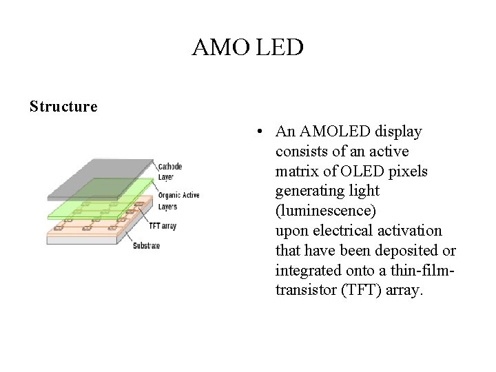
AMO LED Structure • An AMOLED display consists of an active matrix of OLED pixels generating light (luminescence) upon electrical activation that have been deposited or integrated onto a thin-filmtransistor (TFT) array.
AMOLED • Typically, this continuous current flow is controlled by at least two TFTs at each pixel (to trigger the luminescence), with one TFT to start and stop the charging of a storage capacitor and the second to provide a voltage source at the level needed to create a constant current to the pixel, thereby eliminating the need for the very high currents required for passivematrix OLED operation • TFT backplane technology is crucial in the fabrication of AMOLED displays. In AMOLEDs, the two primary TFT backplane technologies, polycrystalline silicon (poly-Si) and amorphous silicon (a-Si), are currently used offering the potential for directly fabricating the active-matrix backplanes at low temperatures (below 150 °C) onto flexible plastic substrates for producing flexible AMOLED displays.
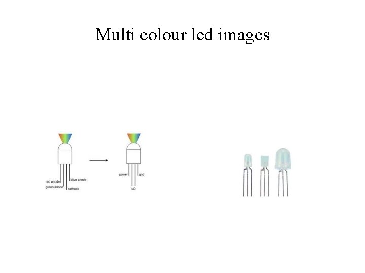
Multi colour led images
Multi colour led • The material used in the semiconducting element of an LED determines its color. • The two main types of LEDs presently used for lighting systems are aluminum gallium indium phosphide (Al. Ga. In. P, sometimes rearranged as Al. In. Ga. P) alloys for red, orange and yellow LEDs; and indium gallium nitride (In. Ga. N) alloys for green, blue and white LEDs. • Slight changes in the composition of these alloys changes the color of the emitted light.