INEL 4207 COMPLEX CMOS LOGIC GATES Complex Gate



![Design CMOS Logic Gate to implement Y=[A(B+C(D+E))]’ Select sizes to obtain same tp Design CMOS Logic Gate to implement Y=[A(B+C(D+E))]’ Select sizes to obtain same tp](https://slidetodoc.com/presentation_image_h/d5410691880d3bc554d0f42bbbf0ee2c/image-13.jpg)


- Slides: 17

INEL 4207 COMPLEX CMOS LOGIC GATES

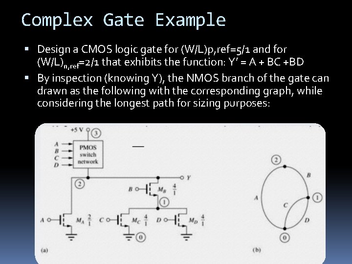
Complex Gate Example Design a CMOS logic gate for (W/L)p, ref=5/1 and for (W/L)n, ref=2/1 that exhibits the function: Y’ = A + BC +BD By inspection (knowing Y), the NMOS branch of the gate can drawn as the following with the corresponding graph, while considering the longest path for sizing purposes:

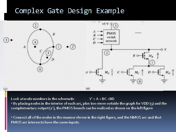
Complex Gate Design Example Look at node numbers in the schematic Y’ = A + BC +BD • By placing nodes in the interior of each arc, plus two more outside the graph for VDD (3) and the complementary output (2’), the PMOS branch can be realized as shown on the left figure • Connect all of the nodes in the manner shown in the right figure, and the NMOS arc and that PMOS arc intersects have the same inputs.

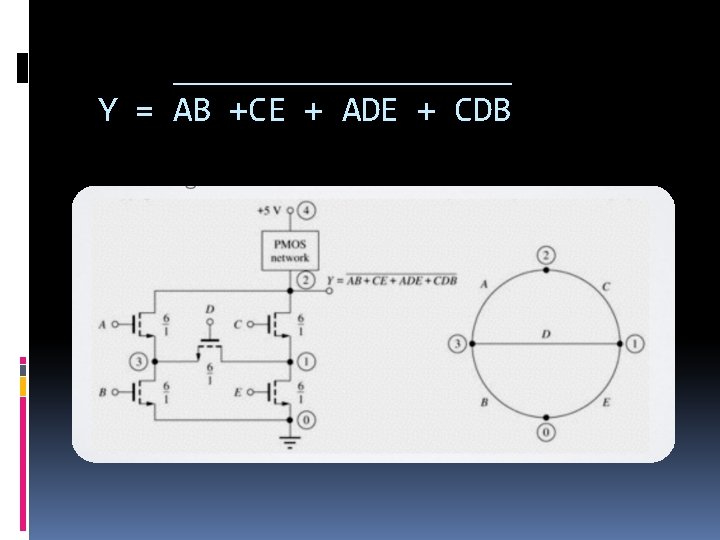
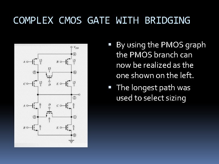
COMPLEX CMOS GATE WITH BRIDGING Design a CMOS gate that implements the following logic function using the same reference inverter sizes as the previous example: _________ Y = AB +CE + ADE + CDB The NMOS branch can be realized in the following manner using bridging NMOS D to implement Y. The corresponding NMOS graph is shown in the next slide.

_________ Y = AB +CE + ADE + CDB

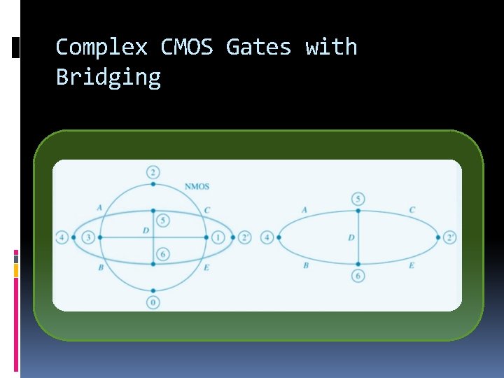
Complex CMOS Gates with Bridging

COMPLEX CMOS GATE WITH BRIDGING By using the PMOS graph the PMOS branch can now be realized as the one shown on the left. The longest path was used to select sizing

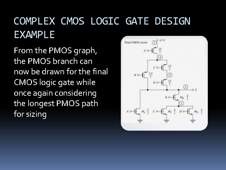
COMPLEX CMOS LOGIC GATE DESIGN EXAMPLE From the PMOS graph, the PMOS branch can now be drawn for the final CMOS logic gate while once again considering the longest PMOS path for sizing

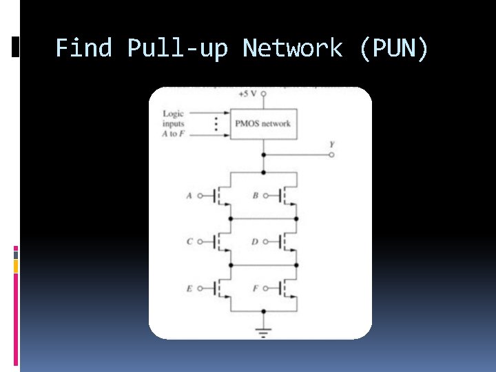
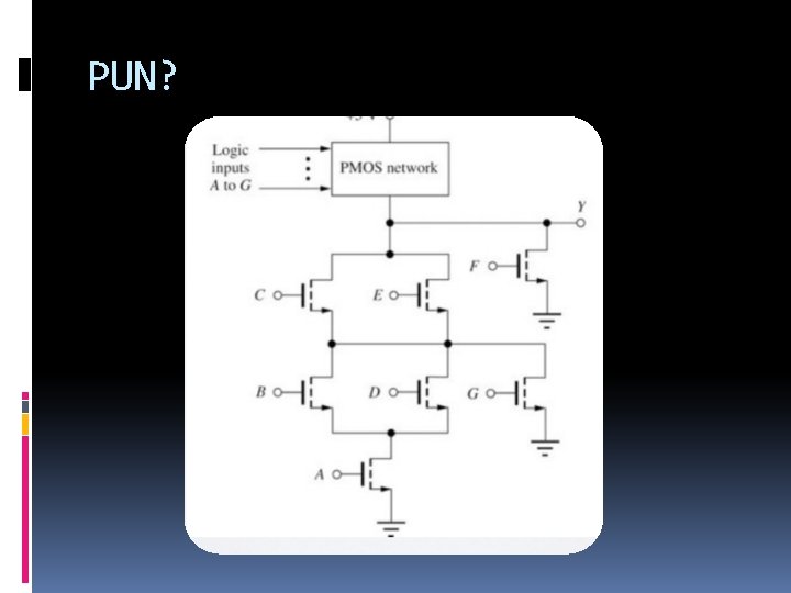
Find Pull-up Network (PUN)

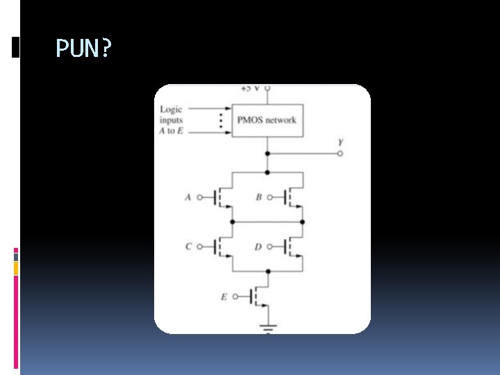
PUN?

PUN?

Design a CMOS logic gate based on the inverter CMOS with bn=bp to implement the following function: Y=(ABC+DE)’ Select transistor sizes to obtain propagation times similar to those of the previous inverter
![Design CMOS Logic Gate to implement YABCDE Select sizes to obtain same tp Design CMOS Logic Gate to implement Y=[A(B+C(D+E))]’ Select sizes to obtain same tp](https://slidetodoc.com/presentation_image_h/d5410691880d3bc554d0f42bbbf0ee2c/image-13.jpg)
Design CMOS Logic Gate to implement Y=[A(B+C(D+E))]’ Select sizes to obtain same tp as in the CMOS inverter

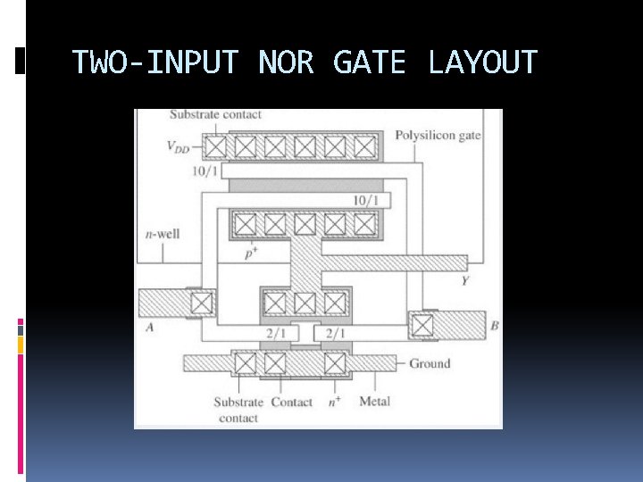
CMOS NOR GATE BODY EFFECT Since the bottom PMOS body contact is not connected to its source, its threshold voltage changes as VSB changes during switching Once v. O = VH is reached, the bottom PMOS is not affected by body effect, thus the total onresistance of the PMOS branch is the same However, the rise time is slowed down due to |VTP| being a function of time

TWO-INPUT NOR GATE LAYOUT

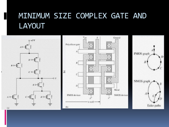
MINIMUM SIZE GATE DESIGN AND PERFORMANCE With CMOS technology, there is a area/delay trade off that needs to be considered If minimum feature sized are used for both devices, then the τPLH will be decreased compared to the symmetrical reference inverter

MINIMUM SIZE COMPLEX GATE AND LAYOUT