DC and RF Modeling of CMOS Schottky Diodes
![Motivation w CMOS Schottky diodes: structures Shallow Trench Separation (STS) [2] Polysilicon Gate Separation Motivation w CMOS Schottky diodes: structures Shallow Trench Separation (STS) [2] Polysilicon Gate Separation](https://slidetodoc.com/presentation_image_h/04eff111751614aa1f87197fec78575e/image-4.jpg)
- Slides: 26

DC and RF Modeling of CMOS Schottky Diodes Wenyuan Zhang, Yang Tang and Yan Wang Tsinghua University June 21 st 2019

Outline w Motivation w Model Description w Parameter Extraction w Model Validation w Model Scalability w Discussion w Conclusion

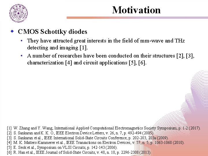
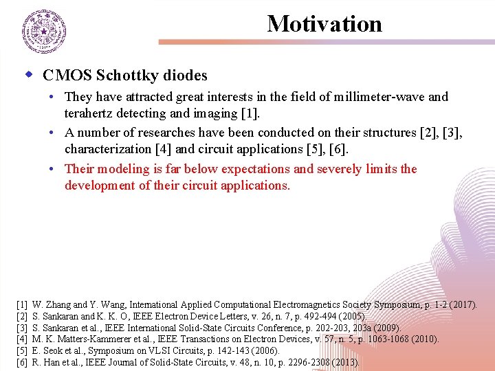
Motivation w CMOS Schottky diodes • They have attracted great interests in the field of mm-wave and THz detecting and imaging [1]. • A number of researches have been conducted on their structures [2], [3], characterization [4] and circuit applications [5], [6]. [1] [2] [3] [4] [5] [6] W. Zhang and Y. Wang, International Applied Computational Electromagnetics Society Symposium, p. 1 -2 (2017). S. Sankaran and K. K. O, IEEE Electron Device Letters, v. 26, n. 7, p. 492 -494 (2005). S. Sankaran et al. , IEEE International Solid-State Circuits Conference, p. 202 -203, 203 a (2009). M. K. Matters-Kammerer et al. , IEEE Transactions on Electron Devices, v. 57, n. 5, p. 1063 -1068 (2010). E. Seok et al. , Symposium on VLSI Circuits, p. 142 -143 (2006). R. Han et al. , IEEE Journal of Solid-State Circuits, v. 48, n. 10, p. 2296 -2308 (2013).
![Motivation w CMOS Schottky diodes structures Shallow Trench Separation STS 2 Polysilicon Gate Separation Motivation w CMOS Schottky diodes: structures Shallow Trench Separation (STS) [2] Polysilicon Gate Separation](https://slidetodoc.com/presentation_image_h/04eff111751614aa1f87197fec78575e/image-4.jpg)
Motivation w CMOS Schottky diodes: structures Shallow Trench Separation (STS) [2] Polysilicon Gate Separation (PGS) [3] Technology 130 nm CMOS Series resistance 13Ω 8Ω Junction capacitance 8 f. F 10 f. F Cut-off frequency 1. 5 THz 2 THz Structure diagram [2] S. Sankaran and K. K. O, IEEE Electron Device Letters, v. 26, n. 7, p. 492 -494 (2005). [3] S. Sankaran et al. , IEEE International Solid-State Circuits Conference, p. 202 -203, 203 a (2009).

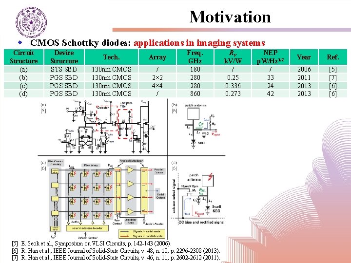
Motivation w CMOS Schottky diodes: applications in imaging systems Circuit Structure (a) (b) (c) (d) Device Structure STS SBD PGS SBD Tech. Array 130 nm CMOS / 2× 2 4× 4 / Freq. GHz 180 280 860 [5] E. Seok et al. , Symposium on VLSI Circuits, p. 142 -143 (2006). [6] R. Han et al. , IEEE Journal of Solid-State Circuits, v. 48, n. 10, p. 2296 -2308 (2013). [7] R. Han et al. , IEEE Journal of Solid-State Circuits, v. 46, n. 11, p. 2602 -2612 (2011). RV k. V/W / 0. 25 0. 336 0. 273 NEP p. W/Hz 1/2 / 33 24 42 Year Ref. 2006 2011 2013 [5] [7] [6]

Motivation w CMOS Schottky diodes • They have attracted great interests in the field of millimeter-wave and terahertz detecting and imaging [1]. • A number of researches have been conducted on their structures [2], [3], characterization [4] and circuit applications [5], [6]. • Their modeling is far below expectations and severely limits the development of their circuit applications. [1] [2] [3] [4] [5] [6] W. Zhang and Y. Wang, International Applied Computational Electromagnetics Society Symposium, p. 1 -2 (2017). S. Sankaran and K. K. O, IEEE Electron Device Letters, v. 26, n. 7, p. 492 -494 (2005). S. Sankaran et al. , IEEE International Solid-State Circuits Conference, p. 202 -203, 203 a (2009). M. K. Matters-Kammerer et al. , IEEE Transactions on Electron Devices, v. 57, n. 5, p. 1063 -1068 (2010). E. Seok et al. , Symposium on VLSI Circuits, p. 142 -143 (2006). R. Han et al. , IEEE Journal of Solid-State Circuits, v. 48, n. 10, p. 2296 -2308 (2013).

Outline w Motivation w Model Description w Parameter Extraction w Model Validation w Model Scalability w Discussion w Conclusion

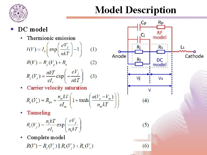
Model Description w DC model • Thermionic emission Vj • Carrier velocity saturation • Tunneling • Complete model Vs V

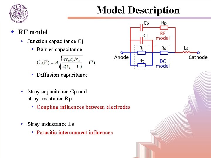
Model Description w RF model • Junction capacitance Cj • Barrier capacitance • Diffusion capacitance • Stray capacitance Cp and stray resistance Rp • Coupling influences between electrodes • Stray inductance Ls • Parasitic interconnect influences

Outline w Motivation w Model Description w Parameter Extraction w Model Validation w Model Scalability w Discussion w Conclusion

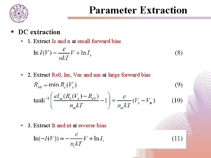
Parameter Extraction w DC extraction • 1. Extract Is and n at small forward bias • 2. Extract Rs 0, Im, Vm and nm at large forward bias • 3. Extract It and nt at reverse bias

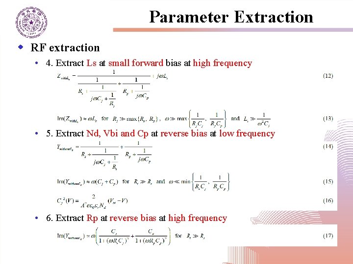
Parameter Extraction w RF extraction • 4. Extract Ls at small forward bias at high frequency • 5. Extract Nd, Vbi and Cp at reverse bias at low frequency • 6. Extract Rp at reverse bias at high frequency

Outline w Motivation w Model Description w Parameter Extraction w Model Validation w Model Scalability w Discussion w Conclusion

Model Validation w Schottky diodes • Fabricated in 65 nm and 130 nm CMOS • Measured up to 67 GHz • Modeling root-mean-square errors < 5%

Model Validation w DC forward characteristics Fig. Measured (red) and modeled (blue) DC characteristics of a single-cell diode in 65 nm CMOS, with 0. 92μm 2 Schottky contact area. Results given by Schottky equation (black) are also given. (a) Forward I-V. (b) Forward R-V. (c) Reverse I-V. (d) Reverse R-V.

Model Validation w DC reverse characteristics Fig. Measured (red) and modeled (blue) DC characteristics of a single-cell diode in 65 nm CMOS, with 0. 92μm 2 Schottky contact area. Results given by Schottky equation (black) are also given. (a) Forward I-V. (b) Forward R-V. (c) Reverse I-V. (d) Reverse R-V.

Model Validation w RF characteristics Fig. Measured (red) and modeled (blue) RF characteristics of a single-cell diode in 65 nm CMOS, with 0. 92μm 2 Schottky contact area. (a) Ctotal=Im(Y)/ω versus bias at different frequencies. (b) Ctotal versus frequency at different biases (from -1. 1 V to 0. 1 V, 0. 1 V step).

Outline w Motivation w Model Description w Parameter Extraction w Model Validation w Model Scalability w Discussion w Conclusion

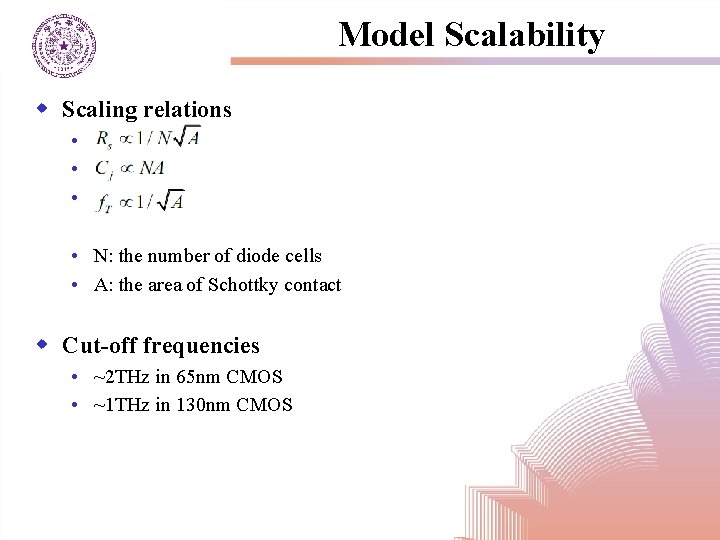
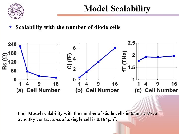
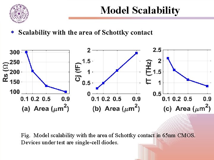
Model Scalability w Scaling relations • • N: the number of diode cells • A: the area of Schottky contact w Cut-off frequencies • ~2 THz in 65 nm CMOS • ~1 THz in 130 nm CMOS

Model Scalability with the number of diode cells Fig. Model scalability with the number of diode cells in 65 nm CMOS. Schottky contact area of a single cell is 0. 185μm 2.

Model Scalability with the area of Schottky contact Fig. Model scalability with the area of Schottky contact in 65 nm CMOS. Devices under test are single-cell diodes.

Outline w Motivation w Model Description w Parameter Extraction w Model Validation w Model Scalability w Discussion w Conclusion

Discussion w On forward capacitance • Abnormal decreasing capacitance with increasing bias • Suggested mechanisms • Capture-emission of carriers by trap levels [8] • Carrier transient response [9] • Carrier polarization [10] • Poole-Frenkel effect [11] • Interface-state effect [12] • We are focusing on the modeling of this behavior [8] L. F. Feng et al. , Appl. Phys. Lett. , vol. 101, no. 23, pp. 233506 -1– 233506 -4, Dec. 2012. [9] K. Bansal et al. , Appl. Phys. Lett. , vol. 105, no. 12, pp. 123503 -1– 123503 -4, Sep. 2014. [10] D. Korucu et al. , J. Optoelectron. Adv. Mater. , vol. 11, no. 2, pp. 192– 196, Feb. 2009. [11] W. Yang et al. , Phys. Status Solidi, vol. 11, no. 3– 4, pp. 714– 717, Apr. 2014. [12] P. Chattopadhyay and D. P. Haldar, Appl. Surf. Sci. , vol. 171, no. 3– 4, pp. 207– 212, Feb. 2001.

Outline w Motivation w Model Description w Parameter Extraction w Model Validation w Model Scalability w Discussion w Conclusion

Conclusion • A complete DC and RF model of CMOS Schottky diodes and its parameter extraction strategy are (will be) established. • With different current transport mechanisms including thermionic emission, carrier velocity saturation and tunneling together with stray capacitance and inductance taken into account, the model predicts accurate results within 5% error, when evaluated with measurements up to 67 GHz in 65 nm and 130 nm CMOS. • The model is scalable with the number of diode cells and the area of Schottky contact. • The model can be applied in mm-wave circuit design.

Thanks for your attention! Wenyuan Zhang, Yang Tang and Yan Wang Tsinghua University June 21 st 2019