Chapter 12 Operational Amplifier Circuits from Microelectronic Circuits



- Slides: 47

Chapter #12: Operational. Amplifier Circuits from Microelectronic Circuits Text by Sedra and Smith Oxford Publishing The College of New Jersey (TCNJ) – ELC 251 Electronics I http: //anthony. deese. googlepages. com Based on Textbook: Microelectronic Circuits by Adel S. Sedra (0195323033)

Introduction § IN THIS CHAPTER YOU WILL LEARN § The design and analysis of the two basic CMOS opamp architectures: the two-stage circuit and the single-stage, folded cascode circuit. § The complete circuit of an analog IC classic: the 741 op-amp. Though 40 years old, the 741 circuit includes so many interesting and useful design techniques that its study is still a must. § Applications of negative feedback within op-amp circuits to achieve bias stability and increased CMRR. The College of New Jersey (TCNJ) – ELC 251 Electronics I http: //anthony. deese. googlepages. com Based on Textbook: Microelectronic Circuits by Adel S. Sedra (0195323033)

Introduction § IN THIS CHAPTER YOU WILL LEARN § How to break a large analog circuit into its recognizable blocks, to be able to make the analysis amendable to a pencil-and-paper approach – which is the best way to learn design. § Some of the modern techniques employed in the design of low-voltage single-supply BJT op amps. § Most importantly, how the different topics we learned about in the preceding chapters come together in the design of the most important analog IC – the op amp. The College of New Jersey (TCNJ) – ELC 251 Electronics I http: //anthony. deese. googlepages. com Based on Textbook: Microelectronic Circuits by Adel S. Sedra (0195323033)

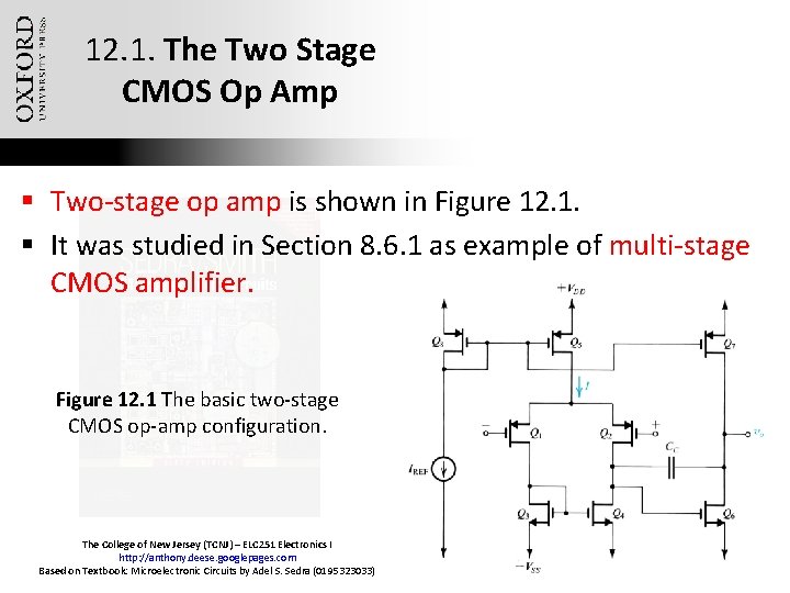
12. 1. The Two Stage CMOS Op Amp § Two-stage op amp is shown in Figure 12. 1. § It was studied in Section 8. 6. 1 as example of multi-stage CMOS amplifier. Figure 12. 1 The basic two-stage CMOS op-amp configuration. The College of New Jersey (TCNJ) – ELC 251 Electronics I http: //anthony. deese. googlepages. com Based on Textbook: Microelectronic Circuits by Adel S. Sedra (0195323033)

12. 1. 1. The Circuit § Two Stages: § Differential Pair Q 1/Q 2. § Biased by current source Q 5 § Fed by a reference current IREF § Current Mirror Load Q 3/Q 4. § Frequency Compensation § Voltage Gain 20 V/V to 60 V/V § Reasonable Common-Mode Rejection Ratio (CMRR) The College of New Jersey (TCNJ) – ELC 251 Electronics I http: //anthony. deese. googlepages. com Based on Textbook: Microelectronic Circuits by Adel S. Sedra (0195323033)

12. 1. 1. Input Common. Mode Range and Output Swing The College of New Jersey (TCNJ) – ELC 251 Electronics I http: //anthony. deese. googlepages. com Based on Textbook: Microelectronic Circuits by Adel S. Sedra (0195323033)

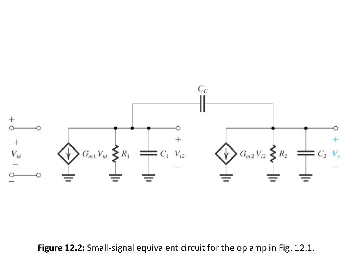
12. 1. 3. Voltage Gain § Consider simplified equivalent circuit model for smallsignal operation of CMOS amplifier. § Figure 12. 2. § Input resistance is practically infinite (Rin). § First-stage transconductance (Gm 1) is equal to values for Q 1 and Q 2. § Since Q 1 and Q 2 are operated at equal bias currents (I/2) and equal overdrive voltages, equation (12. 7) applies. The College of New Jersey (TCNJ) – ELC 251 Electronics I http: //anthony. deese. googlepages. com Based on Textbook: Microelectronic Circuits by Adel S. Sedra (0195323033)

12. 1. 1. Input Common. Mode Range and Output Swing The College of New Jersey (TCNJ) – ELC 251 Electronics I http: //anthony. deese. googlepages. com Based on Textbook: Microelectronic Circuits by Adel S. Sedra (0195323033)

12. 1. 1. Input Common. Mode Range and Output Swing The College of New Jersey (TCNJ) – ELC 251 Electronics I http: //anthony. deese. googlepages. com Based on Textbook: Microelectronic Circuits by Adel S. Sedra (0195323033)

12. 1. 1. Input Common. Mode Range and Output Swing The College of New Jersey (TCNJ) – ELC 251 Electronics I http: //anthony. deese. googlepages. com Based on Textbook: Microelectronic Circuits by Adel S. Sedra (0195323033) Figure 12. 2: Small-signal equivalent circuit for the op amp in Fig. 12. 1.

12. 1. 4. Common-Mode Rejection Ratio § CMRR of two-stage amplifier is determined by first stage § CMRR = [gm 1(ro 2||ro 4)[2 gm 3 RSS] § RSS is output resistance of the bias source Q 5 § CMRR is of the order of (gmro)2 § This is high. § Gmro is proportional to VA/VOV § CMRR is increased if long channels are used. The College of New Jersey (TCNJ) – ELC 251 Electronics I http: //anthony. deese. googlepages. com Based on Textbook: Microelectronic Circuits by Adel S. Sedra (0195323033)

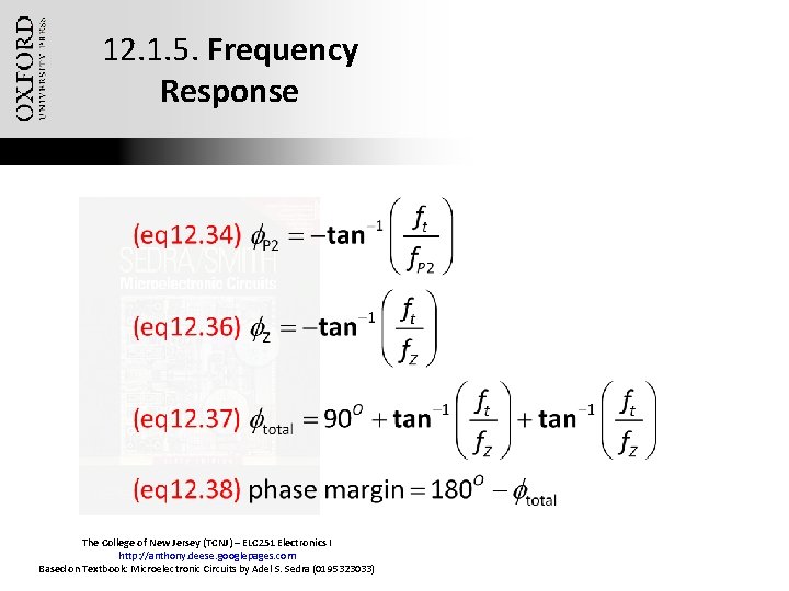
12. 1. 5. Frequency Response The College of New Jersey (TCNJ) – ELC 251 Electronics I http: //anthony. deese. googlepages. com Based on Textbook: Microelectronic Circuits by Adel S. Sedra (0195323033)

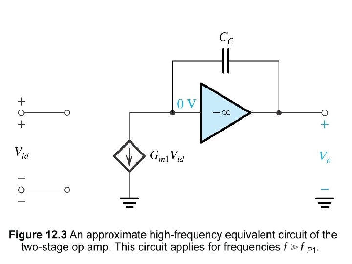
The College of New Jersey (TCNJ) – ELC 251 Electronics I http: //anthony. deese. googlepages. com Based on Textbook: Microelectronic Circuits by Adel S. Sedra (0195323033)

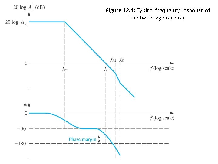
Figure 12. 4: Typical frequency response of the two-stage op amp. The College of New Jersey (TCNJ) – ELC 251 Electronics I http: //anthony. deese. googlepages. com Based on Textbook: Microelectronic Circuits by Adel S. Sedra (0195323033)

12. 1. 5. Frequency Response The College of New Jersey (TCNJ) – ELC 251 Electronics I http: //anthony. deese. googlepages. com Based on Textbook: Microelectronic Circuits by Adel S. Sedra (0195323033)

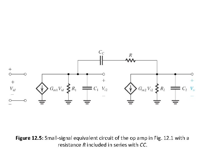
Figure 12. 5: Small-signal equivalent circuit of the op amp in Fig. 12. 1 with a The College of New Jersey (TCNJ) – ELC 251 Electronics I http: //anthony. deese. googlepages. com resistance R included in series with CC. Based on Textbook: Microelectronic Circuits by Adel S. Sedra (0195323033)

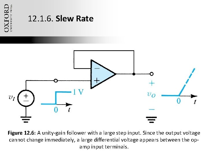
12. 1. 6. Slew Rate Figure 12. 6: A unity-gain follower with a large step input. Since the output voltage cannot change immediately, a large differential voltage appears between the op. The College of New Jersey (TCNJ) – ELC 251 Electronics I http: //anthony. deese. googlepages. com amp input terminals. Based on Textbook: Microelectronic Circuits by Adel S. Sedra (0195323033)

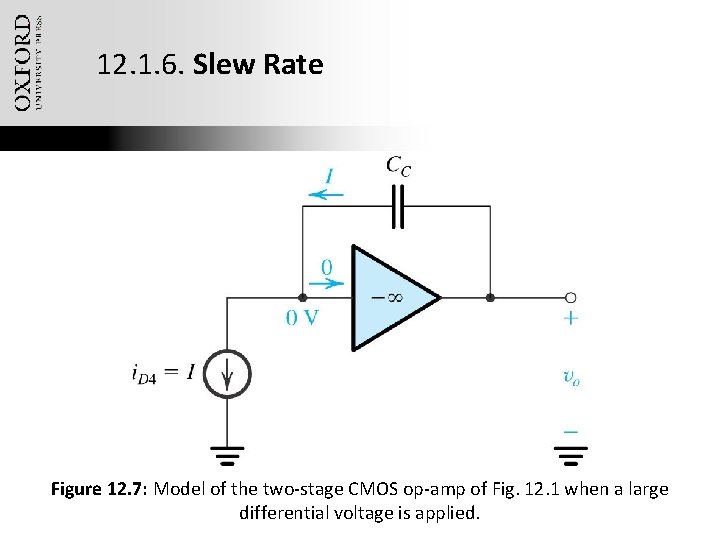
12. 1. 6. Slew Rate Figure 12. 7: the. Electronics two-stage CMOS op-amp of Fig. 12. 1 when a large The College of New. Model Jersey (TCNJ)of – ELC 251 I http: //anthony. deese. googlepages. com differential voltage is applied. Based on Textbook: Microelectronic Circuits by Adel S. Sedra (0195323033)

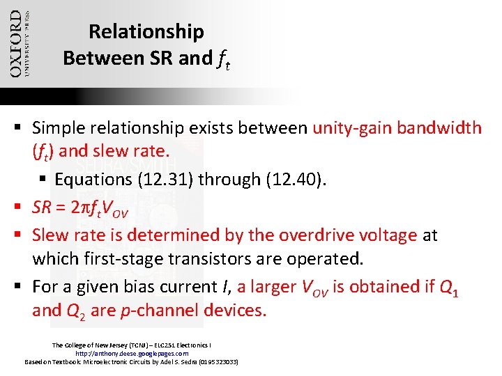
Relationship Between SR and ft § Simple relationship exists between unity-gain bandwidth (ft) and slew rate. § Equations (12. 31) through (12. 40). § SR = 2 pft. VOV § Slew rate is determined by the overdrive voltage at which first-stage transistors are operated. § For a given bias current I, a larger VOV is obtained if Q 1 and Q 2 are p-channel devices. The College of New Jersey (TCNJ) – ELC 251 Electronics I http: //anthony. deese. googlepages. com Based on Textbook: Microelectronic Circuits by Adel S. Sedra (0195323033)

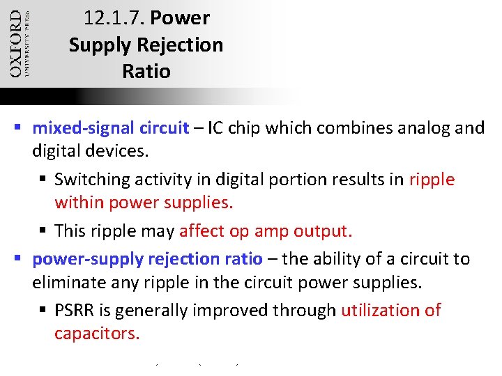
12. 1. 7. Power Supply Rejection Ratio § mixed-signal circuit – IC chip which combines analog and digital devices. § Switching activity in digital portion results in ripple within power supplies. § This ripple may affect op amp output. § power-supply rejection ratio – the ability of a circuit to eliminate any ripple in the circuit power supplies. § PSRR is generally improved through utilization of capacitors. The College of New Jersey (TCNJ) – ELC 251 Electronics I http: //anthony. deese. googlepages. com Based on Textbook: Microelectronic Circuits by Adel S. Sedra (0195323033)

12. 1. 7. Power Supply Rejection Ratio The College of New Jersey (TCNJ) – ELC 251 Electronics I http: //anthony. deese. googlepages. com Based on Textbook: Microelectronic Circuits by Adel S. Sedra (0195323033)

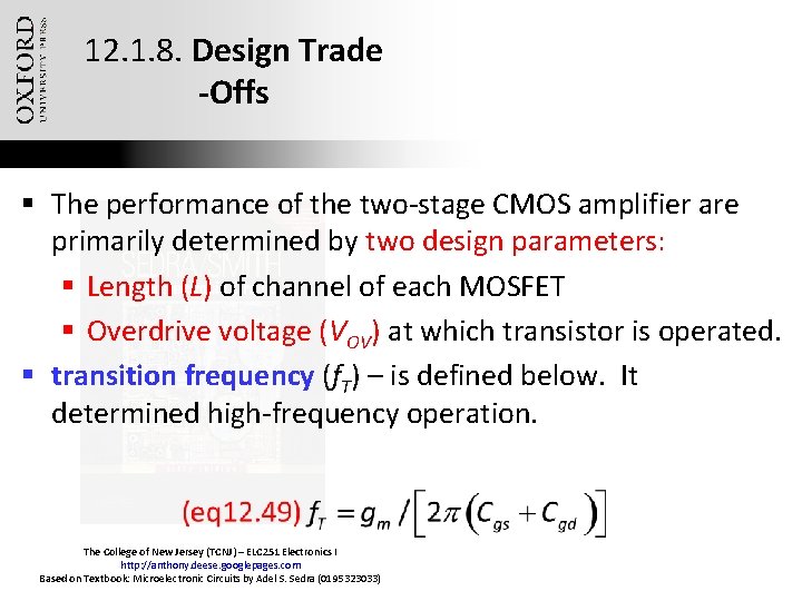
12. 1. 8. Design Trade -Offs § The performance of the two-stage CMOS amplifier are primarily determined by two design parameters: § Length (L) of channel of each MOSFET § Overdrive voltage (VOV) at which transistor is operated. § transition frequency (f. T) – is defined below. It determined high-frequency operation. The College of New Jersey (TCNJ) – ELC 251 Electronics I http: //anthony. deese. googlepages. com Based on Textbook: Microelectronic Circuits by Adel S. Sedra (0195323033)

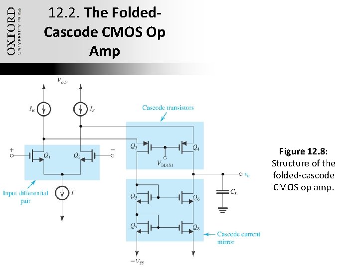
12. 2. The Folded. Cascode CMOS Op Amp Figure 12. 8: Structure of the folded-cascode CMOS op amp. The College of New Jersey (TCNJ) – ELC 251 Electronics I http: //anthony. deese. googlepages. com Based on Textbook: Microelectronic Circuits by Adel S. Sedra (0195323033)

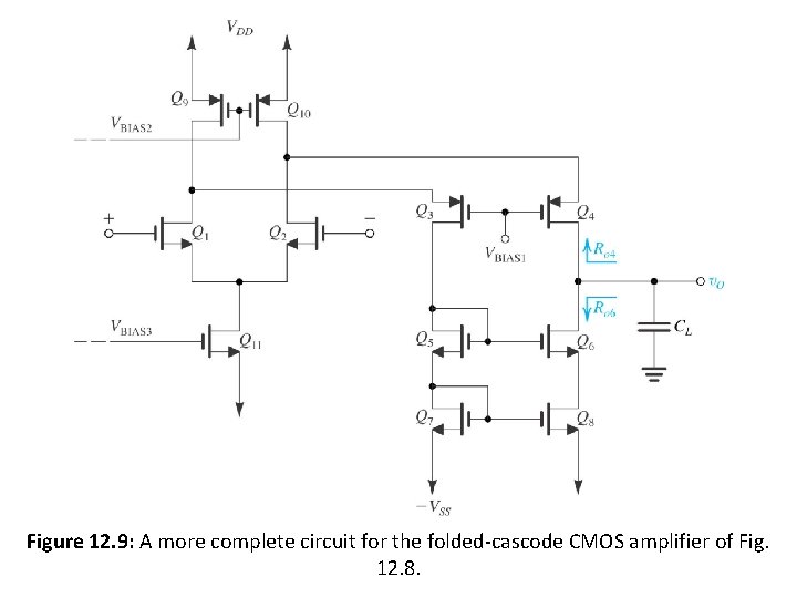
12. 7. 1. The Circuit Figure. The 12. 9: ANew more complete circuit for the folded-cascode CMOS amplifier of Fig. College of Jersey (TCNJ) – ELC 251 Electronics I http: //anthony. deese. googlepages. com Based on Textbook: Microelectronic Circuits by Adel S. Sedra (0195323033)12. 8.

12. 2. 2. Input Common. Mode Range and Output Swing The College of New Jersey (TCNJ) – ELC 251 Electronics I http: //anthony. deese. googlepages. com Based on Textbook: Microelectronic Circuits by Adel S. Sedra (0195323033)

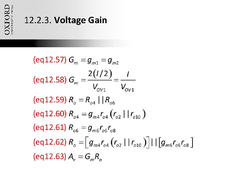
12. 2. 3. Voltage Gain The College of New Jersey (TCNJ) – ELC 251 Electronics I http: //anthony. deese. googlepages. com Based on Textbook: Microelectronic Circuits by Adel S. Sedra (0195323033)

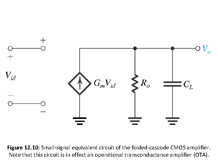
12. 7. 1. The Circuit Figure. The 12. 10: equivalent circuit of the folded-cascode CMOS amplifier. College of Small-signal New Jersey (TCNJ) – ELC 251 Electronics I http: //anthony. deese. googlepages. com Note this circuit. Circuits is in effect an operational transconductance amplifier (OTA). Based onthat Textbook: Microelectronic by Adel S. Sedra (0195323033)

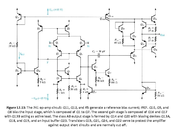
12. 3. The 741 Op. Amp Circuit § Sections 12. 3. through 12. 6 focus on the 741 op-amp circuit. § Figure 12. 13. provides a circuit schematic. § The design uses many transistors, few resistors. § 741 requires two power supplies. § VCC = VEE = 15 V The College of New Jersey (TCNJ) – ELC 251 Electronics I http: //anthony. deese. googlepages. com Based on Textbook: Microelectronic Circuits by Adel S. Sedra (0195323033)

12. 7. 1. The Circuit Figure 12. 13: The 741 op-amp circuit: Q 11, Q 12, and R 5 generate a reference bias current; IREF. Q 10, Q 9, and Q 8 bias the input stage, which is composed of Q 1 to Q 7. The second gain stage is composed of Q 16 and Q 17 with Q 13 B acting as active load. The class AB output stage is formed by Q 14 and Q 20 with biasing devices Q 13 A, The College Newan Jersey (TCNJ)buffer – ELC 251 Q 23. Electronics I Q 18, and Q 19, ofand input Transistors Q 15, Q 21, Q 24, and Q 22 serve to protect the amplifier http: //anthony. deese. googlepages. com against short circuits and are normally cut off. Based on Textbook: Microelectronic Circuits by Adeloutput S. Sedra (0195323033)

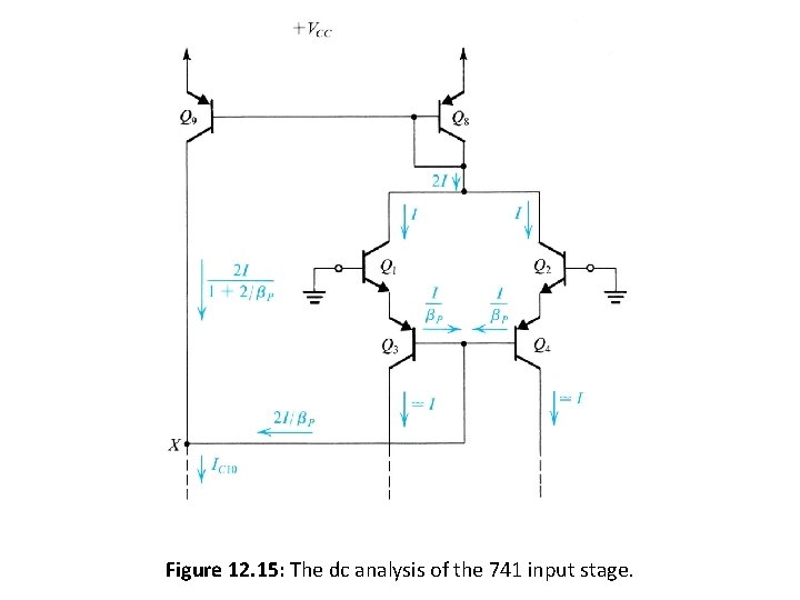
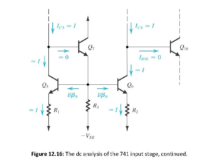
12. 3. 3. The Input Stage § 741 consists of three-stages: § Input Differential Stage (Q 1 through Q 7) § Emitter Followers: Q 1, Q 2 § Differential Common-Base: Q 3, Q 4 § Load Circuit: Q 5, Q 6, Q 7 § Biasing: Q 8, Q 9, Q 10 § Intermediate Single-Ended High-Gain Stage § Output-Buffering Stage (other transistors) The College of New Jersey (TCNJ) – ELC 251 Electronics I http: //anthony. deese. googlepages. com Based on Textbook: Microelectronic Circuits by Adel S. Sedra (0195323033)

12. 3. 4. The Second Stage § Consists of Q 16, Q 17, and Q 13 B § Emitter Follower: Q 16 § Common-Emitter: Q 17 § Load: Q 13 B § Output of second stage is taken at collector of Q 17. § Capacitor CC is connected in feedback path of second stage. § Frequency compensation using Miller Technique. The College of New Jersey (TCNJ) – ELC 251 Electronics I http: //anthony. deese. googlepages. com Based on Textbook: Microelectronic Circuits by Adel S. Sedra (0195323033)

12. 3. 5. The Output Stage § Provides low output resistance. § Able to supply relatively large load current. § With minimal power dissipation. § Consists of Q 14 and Q 20. § Complementary pair. § Transistors Q 18 and Q 19 are fed by current source Q 13 A and bias transistors Q 14 and Q 20. The College of New Jersey (TCNJ) – ELC 251 Electronics I http: //anthony. deese. googlepages. com Based on Textbook: Microelectronic Circuits by Adel S. Sedra (0195323033)

12. 3. 6. Device Parameters § npn: IS = 10 -14 A, b = 200, VA = 125 V § pnp: IS = 10 -14 A, b = 50, VA = 50 V § Q 13 A and Q 13 B: ISA = 0. 25(10 -14)A, ISB = 0. 75(10 -14)A § These devices are non-standard. § Q 14 and Q 20 will be assumed to have area three times of the standard device – for increased loading. The College of New Jersey (TCNJ) – ELC 251 Electronics I http: //anthony. deese. googlepages. com Based on Textbook: Microelectronic Circuits by Adel S. Sedra (0195323033)

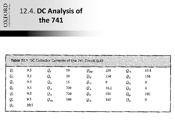
12. 4. DC Analysis of the 741 The College of New Jersey (TCNJ) – ELC 251 Electronics I http: //anthony. deese. googlepages. com Based on Textbook: Microelectronic Circuits by Adel S. Sedra (0195323033)

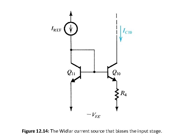
12. 7. 1. The Circuit The College of New Jersey (TCNJ) – ELC 251 Electronics I http: //anthony. deese. googlepages. com Based on Textbook: Microelectronic Circuits by Adel S. Sedra (0195323033) Figure 12. 14: The Widlar current source that biases the input stage.

12. 7. 1. The Circuit The College of New Jersey (TCNJ) – ELC 251 Electronics I http: //anthony. deese. googlepages. com Based on Textbook: Microelectronic Circuits by Adel S. Sedra (0195323033) Figure 12. 15: The dc analysis of the 741 input stage.

12. 7. 1. The Circuit The College of New Jersey (TCNJ) – ELC 251 Electronics I http: //anthony. deese. googlepages. com Based on Textbook: Microelectronic Circuits by Adel S. Sedra (0195323033) Figure 12. 16: The dc analysis of the 741 input stage, continued.

12. 4. DC Analysis of the 741 The College of New Jersey (TCNJ) – ELC 251 Electronics I http: //anthony. deese. googlepages. com Based on Textbook: Microelectronic Circuits by Adel S. Sedra (0195323033)

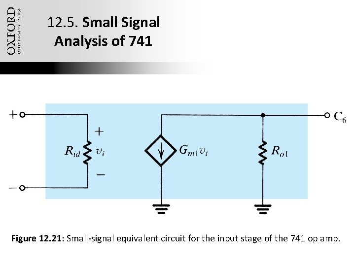
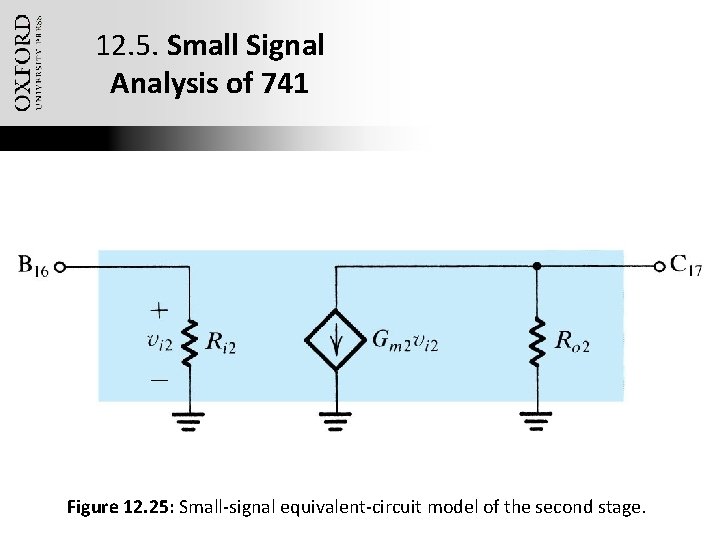
12. 5. Small Signal Analysis of 741 § One may use small-signal analysis (as in previous chapters) to analyze linear behavior of the 741. § Figures 12. 18 – 12. 21 describe this process for input stage. § Figures 12. 25 – 12. 27 describe this process for gain stage. § Figures 12. 28 – 12. 30 describe this process for output stage. The College of New Jersey (TCNJ) – ELC 251 Electronics I http: //anthony. deese. googlepages. com Based on Textbook: Microelectronic Circuits by Adel S. Sedra (0195323033)

12. 5. Small Signal Analysis of 741 Figure The 12. 21: Small-signal equivalent circuit for the input stage of the 741 op amp. College of New Jersey (TCNJ) – ELC 251 Electronics I http: //anthony. deese. googlepages. com Based on Textbook: Microelectronic Circuits by Adel S. Sedra (0195323033)

12. 5. Small Signal Analysis of 741 The College of New Jersey (TCNJ) – ELC 251 Electronics I http: //anthony. deese. googlepages. com Based on Textbook: Microelectronic Circuits by Adel S. Sedra (0195323033) Figure 12. 25: Small-signal equivalent-circuit model of the second stage.

Summary § Most CMOS op-amps are designed to operate as part of a VLSI circuit and thus required to drive only small capacitive loads. Therefore, most do not have a lowoutput-resistance stage. § There are basically two approaches to the design of CMOS op-amps: a two-stage configuration and a singlestage topology using the folded-cascode circuit. § In the two-stage CMOS op-amp, approximately equal gains are realized in the two stages. The College of New Jersey (TCNJ) – ELC 251 Electronics I http: //anthony. deese. googlepages. com Based on Textbook: Microelectronic Circuits by Adel S. Sedra (0195323033)

Summary § The threshold mismatch together with the low transconductance of the input stage result in a larger input offset voltage for the CMOS op-amps than for bipolar units. § Miller compensation is employed in the two-stage CMOS op-amp, but a series resistor is required to place the transmission zero at either s = infinity or on the negative real axis. § CMOS op-amps have better slew rates (than alt’s). The College of New Jersey (TCNJ) – ELC 251 Electronics I http: //anthony. deese. googlepages. com Based on Textbook: Microelectronic Circuits by Adel S. Sedra (0195323033)

Summary § Use of the cascode configuration increases the gain of a CMOS amplifier stage by about two orders of magnitude, thus making possible a single-stage op-amp. § The dominant pole of the folded-cascode op-amp is determined by the total capacitance at the output CL. Increasing CL improves the phase margin at the expense of reducing bandwidth. § By using two complementary input differential pairs in parallel, the common-mode range may be extended. The College of New Jersey (TCNJ) – ELC 251 Electronics I http: //anthony. deese. googlepages. com Based on Textbook: Microelectronic Circuits by Adel S. Sedra (0195323033)

Summary § The output voltage swing of the folded-cascode op-amp may be extended by utilizing a wide-swing current mirror in place of the cascode mirror. § The internal circuit of the 741 op-amp embodies many of the design techniques employed in bipolar analog integrated circuits. § The 741 circuit consists of an input differential stage, a high-gain single-ended second stage, and a class AB output stage. It is the basis for many other devices. The College of New Jersey (TCNJ) – ELC 251 Electronics I http: //anthony. deese. googlepages. com Based on Textbook: Microelectronic Circuits by Adel S. Sedra (0195323033)

Summary § To obtain low input offset voltage and current, and high CMRR, the 741 input stage is designed to be perfectly balanced. The CMRR is increased by common-mode feedback, which also stabilizes the dc operating point. § To obtain high input resistance and low input bias current, the input stage of the 741 is operated as a very low current level. § The use of Miller Frequency compensation in the 741 circuit enables locating the dominant pole at a very low frequency, while utilizing a relatively small compensating capacitance. The College of New Jersey (TCNJ) – ELC 251 Electronics I http: //anthony. deese. googlepages. com Based on Textbook: Microelectronic Circuits by Adel S. Sedra (0195323033)

Summary § Two-stage op-amps may be modeled as a transconductance amplifier feeding an ideal integrator with CC as the integrating capacitor. § The slew rate of a two-stage op-amp is determined by the first-stage bias current and frequency-compensation capacitor. § While the 741 and similar op-amps nominally operate from 15 V power supplies, modern BJT op-amps typically utilize a single ground-referenced supply of only 2 or 3 V. The College of New Jersey (TCNJ) – ELC 251 Electronics I http: //anthony. deese. googlepages. com Based on Textbook: Microelectronic Circuits by Adel S. Sedra (0195323033)