LatchUP What is Latchup Latchup is a condition
- Slides: 12
Latch-UP What is Latch-up? • Latch-up is a condition that can occur in a circuit fabricated in a bulk CMOS technology. When a chip is in a state of latch – up it draws a large current from the power supply but does not function in response to input stimuli. A chip may be operating normally and then enter a state of latch-up; in this case , removing and reconnecting the power supply may restore operations.
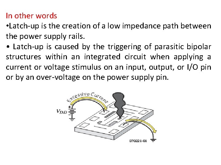
In other words • Latch-up is the creation of a low impedance path between the power supply rails. • Latch-up is caused by the triggering of parasitic bipolar structures within an integrated circuit when applying a current or voltage stimulus on an input, output, or I/O pin or by an over-voltage on the power supply pin.
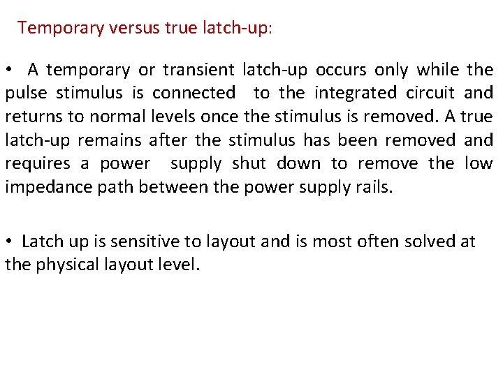
Temporary versus true latch-up: • A temporary or transient latch-up occurs only while the pulse stimulus is connected to the integrated circuit and returns to normal levels once the stimulus is removed. A true latch-up remains after the stimulus has been removed and requires a power supply shut down to remove the low impedance path between the power supply rails. • Latch up is sensitive to layout and is most often solved at the physical layout level.
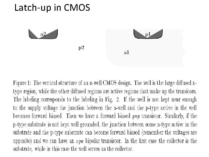
Latch-up in CMOS
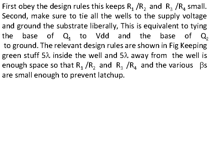
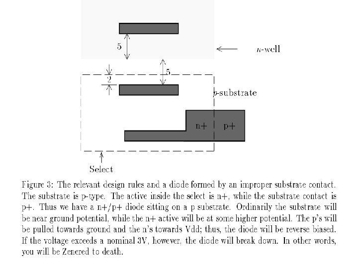
First obey the design rules this keeps R 1 /R 2 and R 3 /R 4 small. Second, make sure to tie all the wells to the supply voltage and ground the substrate liberally, This is equivalent to tying the base of Q 1 to Vdd and the base of Q 2 to ground. The relevant design rules are shown in Fig Keeping green stuff 5 inside the well and 5 away from the well is enough space so that R 1 /R 2 and R 3 /R 4 and the various s are small enough to prevent latchup.
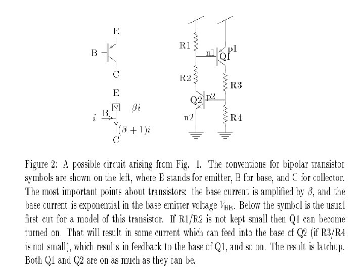
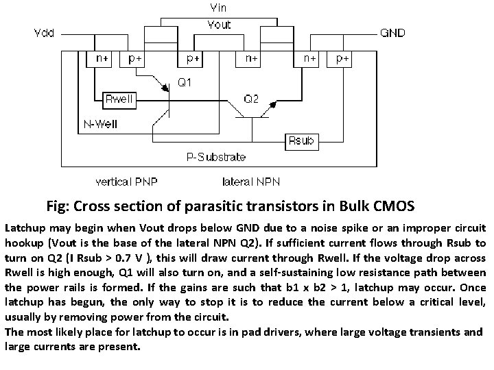
Fig: Cross section of parasitic transistors in Bulk CMOS Latchup may begin when Vout drops below GND due to a noise spike or an improper circuit hookup (Vout is the base of the lateral NPN Q 2). If sufficient current flows through Rsub to turn on Q 2 (I Rsub > 0. 7 V ), this will draw current through Rwell. If the voltage drop across Rwell is high enough, Q 1 will also turn on, and a self sustaining low resistance path between the power rails is formed. If the gains are such that b 1 x b 2 > 1, latchup may occur. Once latchup has begun, the only way to stop it is to reduce the current below a critical level, usually by removing power from the circuit. The most likely place for latchup to occur is in pad drivers, where large voltage transients and large currents are present.
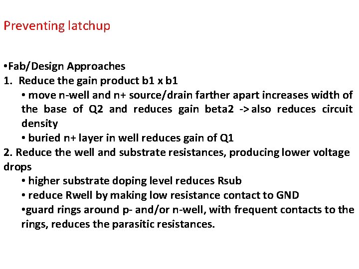
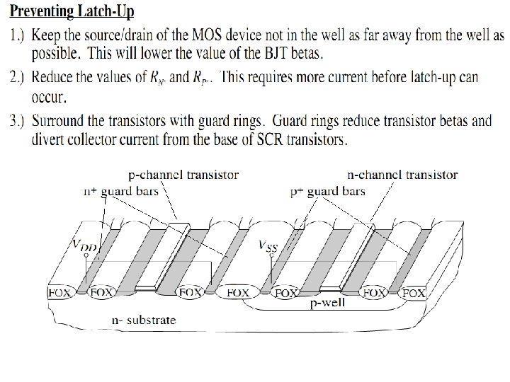
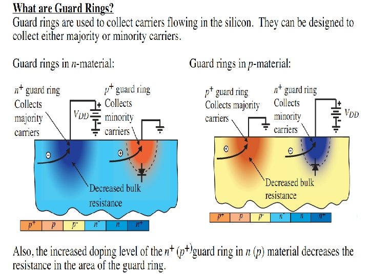
Preventing latchup • Fab/Design Approaches 1. Reduce the gain product b 1 x b 1 • move n well and n+ source/drain farther apart increases width of the base of Q 2 and reduces gain beta 2 > also reduces circuit density • buried n+ layer in well reduces gain of Q 1 2. Reduce the well and substrate resistances, producing lower voltage drops • higher substrate doping level reduces Rsub • reduce Rwell by making low resistance contact to GND • guard rings around p and/or n well, with frequent contacts to the rings, reduces the parasitic resistances.
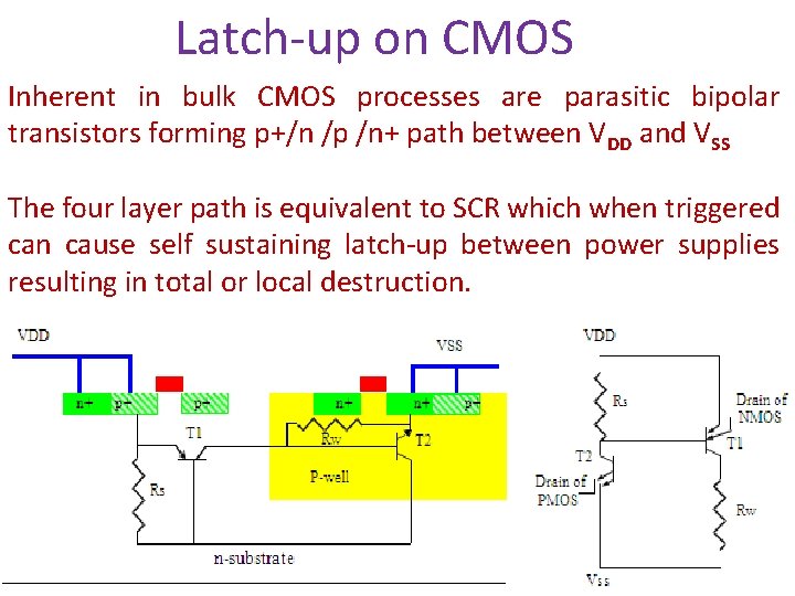
Latch-up on CMOS Inherent in bulk CMOS processes are parasitic bipolar transistors forming p+/n /p /n+ path between VDD and VSS The four layer path is equivalent to SCR which when triggered can cause self sustaining latch-up between power supplies resulting in total or local destruction.