Chapter 9 Logic Families and Their Characteristics 1




- Slides: 62
Chapter 9 Logic Families and Their Characteristics 1
Objectives You should be able to: Analyze internal circuitry of a TTL NAND gate for both HIGH and LOW output states. n Determine IC input and output voltage and current ratings from the manufacturer’s data manual. n Explain gate loading, fan-out, noise margin, and time parameters. n 2
Objectives (Continued) Design wired-output circuits using opencollector TTL gates. n Discuss the differences and proper use of the various subfamilies within both TTL and CMOS ICs. n Describe the reasoning and various techniques for interfacing among the TTL, CMOS, and ECL families of ICs. n 3
Digital Logic Families n Three commonly used families: TTL (transistor-transistor logic) n CMOS (complementary metal oxide semiconductor) n ECL (emitter-coupled logic) n n Subfamilies within each family n n Different speed, power consumption, voltage and current levels, and temperature ranges There are standardized numbering schemes but prefixes may differ
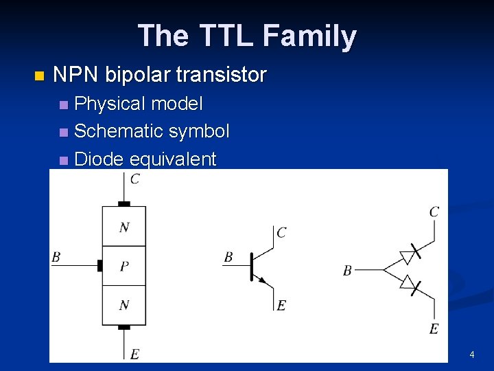
The TTL Family n NPN bipolar transistor Physical model n Schematic symbol n Diode equivalent n 4
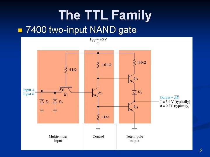
The TTL Family Two-input NAND gate n Multi-emitter transistor n Totem-pole output stage n HIGH level output typically 3. 4 V n LOW level output typically 0. 3 V n 5
The TTL Family n 7400 two-input NAND gate 6
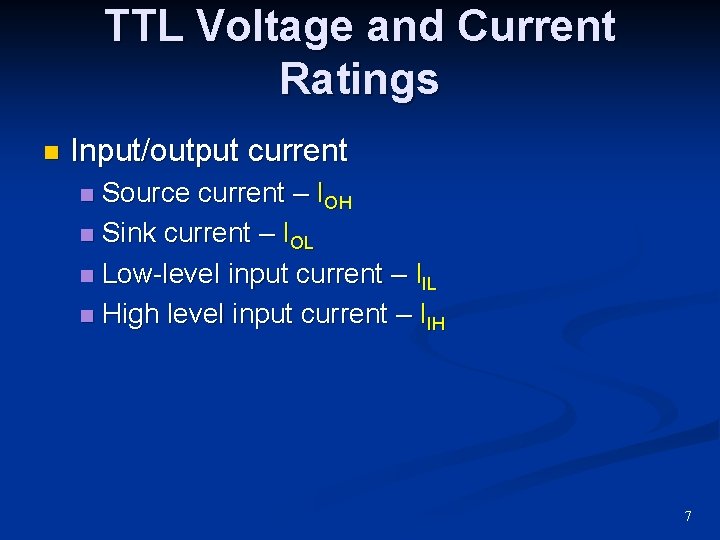
TTL Voltage and Current Ratings n Input/output current Source current – IOH n Sink current – IOL n Low-level input current – IIL n High level input current – IIH n 7
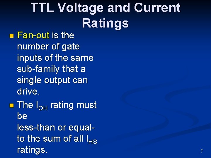
TTL Voltage and Current Ratings Fan-out is the number of gate inputs of the same sub-family that a single output can drive. n The IOH rating must be less-than or equalto the sum of all IHS ratings. n 7
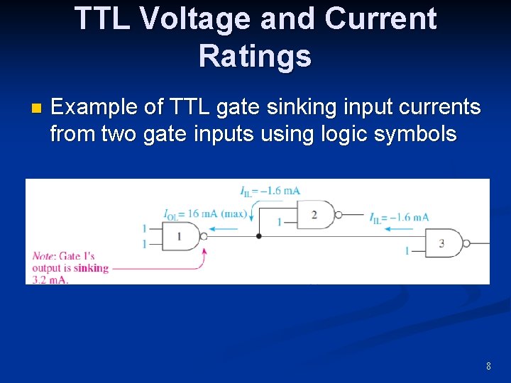
TTL Voltage and Current Ratings n Example of TTL gate sinking input currents from two gate inputs using logic symbols 8
TTL Voltage and Current Ratings n Example of TTL gate sinking input currents from two gate inputs using schematic symbols 9
TTL Voltage and Current Ratings n Example of TTL gate sourcing current to two gate inputs using logic symbols 10
TTL Voltage and Current Ratings n Example of TTL gate sourcing current to two gate inputs using schematic symbols 11
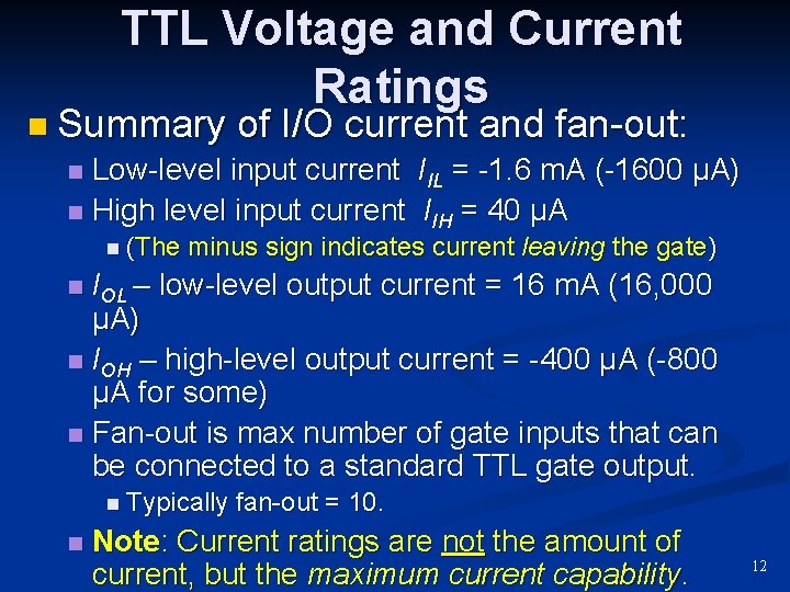
TTL Voltage and Current Ratings n Summary of I/O current and fan-out: Low-level input current IIL = -1. 6 m. A (-1600 μA) n High level input current IIH = 40 μA n n (The n IOL – minus sign indicates current leaving the gate) low-level output current = 16 m. A (16, 000 μA) n IOH – high-level output current = -400 μA (-800 μA for some) n Fan-out is max number of gate inputs that can be connected to a standard TTL gate output. n Typically n fan-out = 10. Note: Current ratings are not the amount of current, but the maximum current capability. 12
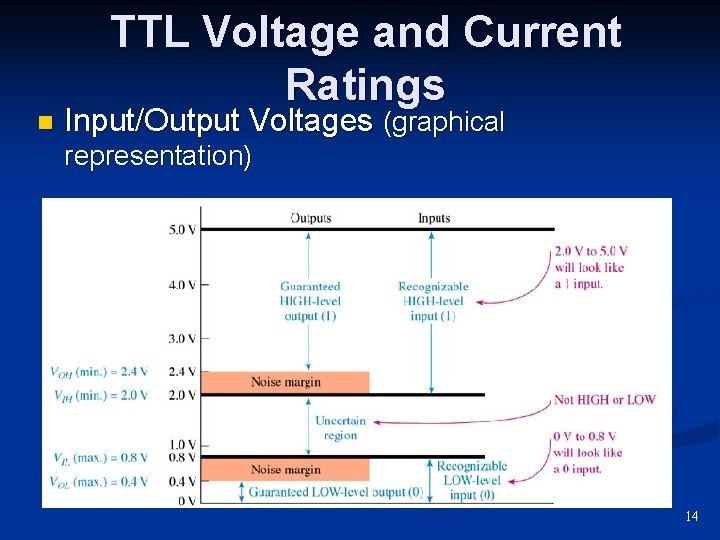
n TTL Voltage and Current Ratings Input/Output Voltages (graphical representation) 14
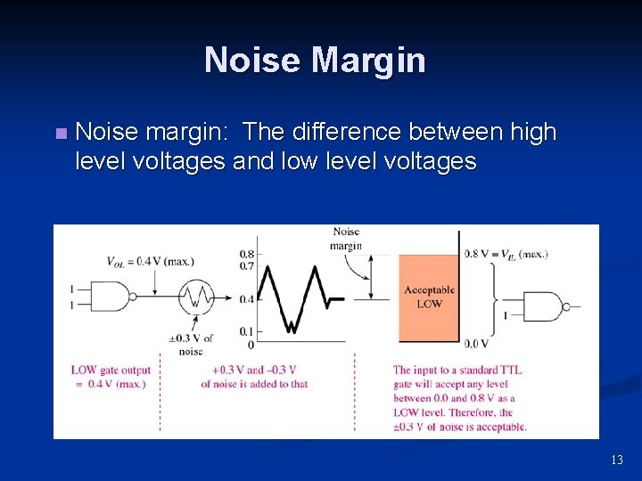
Noise Margin n Noise margin: The difference between high level voltages and low level voltages 13
n TTL Voltage and Current Ratings Input/Output Voltages and noise margin 14
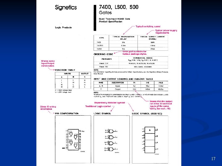
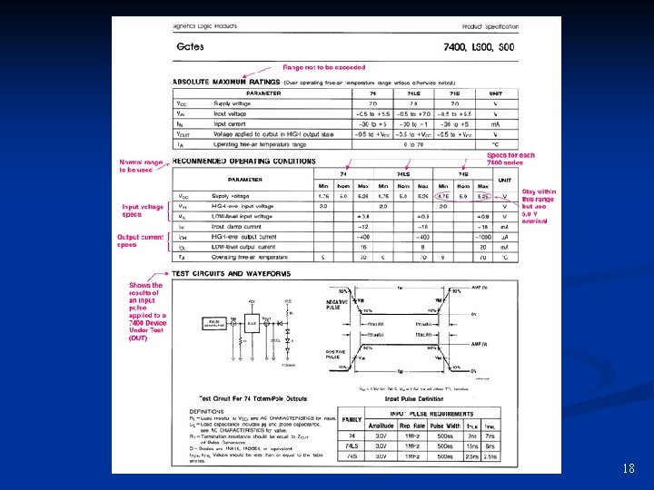
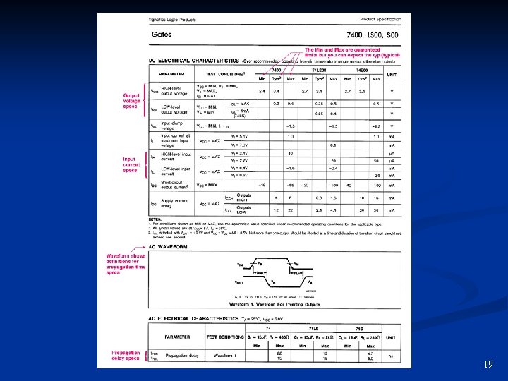
Discussion Point n Locate the voltage and current ratings covered so far on the following typical data sheet (Figure 9. 8). 16
17
18
19
Pulse-Time Parameters Rise Time (tr) – Measured from 10% level to 90% level n Fall Time (tf) – Measured from 90% level to 10% level n 20
Propagation Delay n Propagation Delay (t. PLH and t. PHL) n Determined by transistor switching speed 22
Power Dissipation Total power supplied to the IC power supply terminals n Assume 50% duty cycle. n PD = VCC x ICC(av) n 23
Open-Collector Outputs Upper transistor is removed n Can sink current but cannot source current n
Open-Collector Outputs n To get a TTL OC output or a CMOS OD output to produce a HIGH, a pull-up resistor is required.
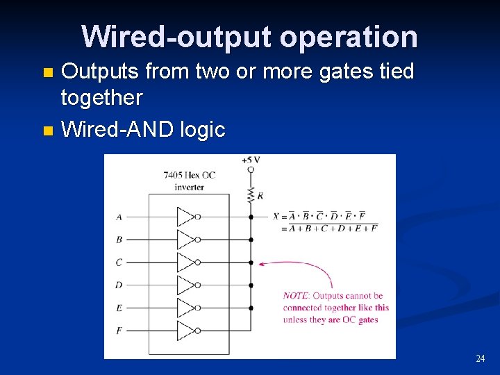
Wired-output operation Outputs from two or more gates tied together n Wired-AND logic n 24
Other TTL Considerations n Disposition of unused inputs and unused gates: Open inputs degrade noise immunity n AND and NAND – tied HIGH n OR and NOR – tied to ground n Unused gates – force outputs HIGH n 25
Other TTL Considerations n Power supply decoupling TTL logic tends to produce spikes on the VCC line n Connecting a 0. 01 to 0. 1 F capacitor between VCC and ground pins n n Reduces EMI radiation n Reduces effect of voltage spikes from power supply n Should installed close to the IC 26
Improved TTL Series n 74 HXX series Half the propagation delay n Double the power consumption n n 74 LXX series Twice the propagation delay n Half the power consumption n In both cases the speed-power product remained about the same. n In most cases both have been replaced by Schottky TTL and CMOS. n 27
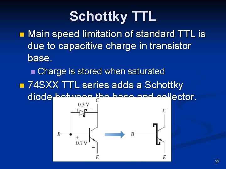
Schottky TTL n Main speed limitation of standard TTL is due to capacitive charge in transistor base. n n Charge is stored when saturated 74 SXX TTL series adds a Schottky diode between the base and collector. 27
Schottky TTL n Lower-power Schottky (LS) Power consumption significantly reduced n Speed-power product 1/3 of 74 SXX series and 1/5 of 74 XX series n n Advanced low-power Schottky (ALS) Propagation delay dropped from 9 to 4 ns n Power dissipation from 2 to 1 m. W per gate n More expensive n n Fast (F) Propagation lowered to under 3 ns. n Device size dramatically reduced n 27
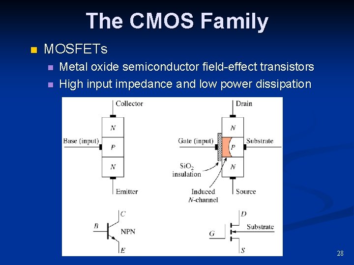
The CMOS Family n MOSFETs n n Metal oxide semiconductor field-effect transistors High input impedance and low power dissipation 28
The CMOS Family n N-Channel MOSFET Built on P material n Normally OFF n Positive gate voltage induces the Nchannel n n P-channel MOSFET n n Channel is formed by a positive gate voltage Three major MOS families PMOS: P-channel n NMOS: N-channel n 30
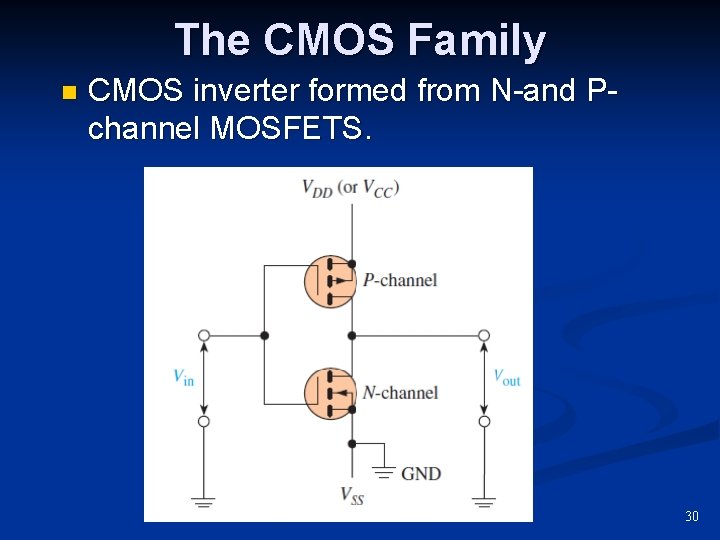
The CMOS Family n CMOS inverter formed from N-and Pchannel MOSFETS. 30
Other CMOS Gates 30
Handling CMOS devices n Avoid electrostatic discharge Ground work station, test equipment and soldering irons n Wear a wrist strap n Don’t connect input signals with power off n Connected unused inputs to VDD n Don’t remove IC with power on n 30
CMOS Availability 4000 series - original CMOS line n 40 H 00 series - faster n 74 C 00 series - pin compatible with TTL n 74 HC 00 and 74 HCT 00 series n n Speedy, less power, pin compatible, greater noise immunity and temperature operating range 30
CMOS Availability 74 - Bi. CMOS series - low power and high speed n 74 -Low Voltage series n See appendix B n Nominal supply voltage of 3. 3 V n n 74 AHC and 74 AHCT series Superior speed n Low power consumption n High output drive current n 31
CMOS Availability n 74 AVC advanced very-low-voltage CMOS logic Faster speed (maximum 2 ns) n Very low operating voltages n n 3. 3 n V, 2. 5 V, 1. 8 V, 1. 5 V and 1. 2 V Dynamic output control n Adjusts output impedance to minimize overshoot and undershoot 32
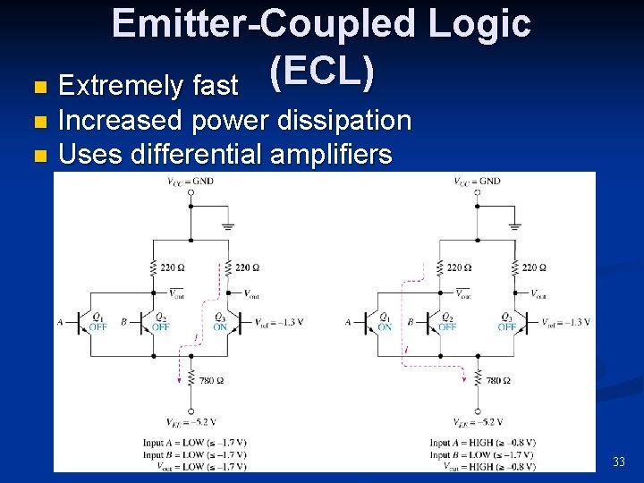
Emitter-Coupled Logic (ECL) n Extremely fast Increased power dissipation n Uses differential amplifiers n Figure 9 -22 33
Developing Technologies n Newer technologies Integrated injection logic (I 2 L) n Silicon-on-sapphire (SOS) n Gallium arsenide (Ga. As) n Josephson junction circuits n n In all cases the goal is higher frequencies and increased density. 34
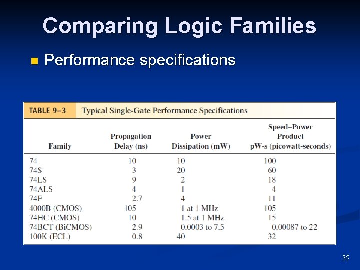
Comparing Logic Families n Performance specifications 35
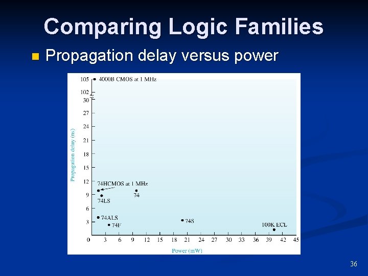
Comparing Logic Families n Propagation delay versus power 36
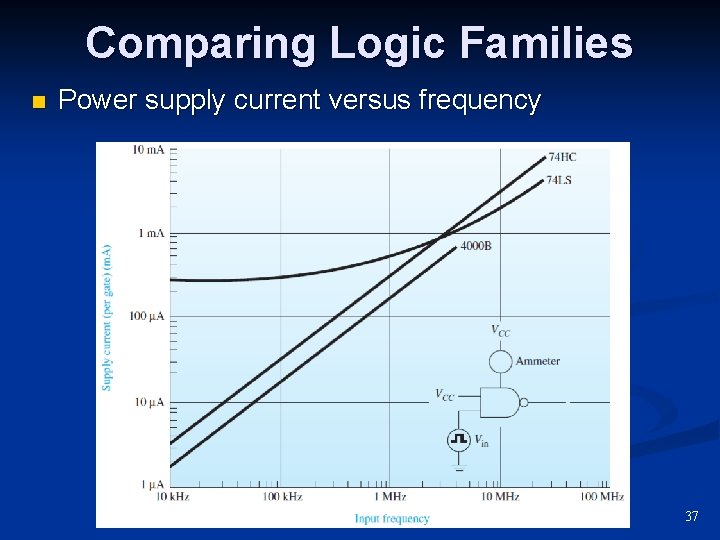
Comparing Logic Families n Power supply current versus frequency 37
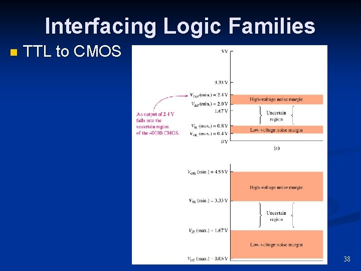
Interfacing Logic Families n TTL to CMOS 38
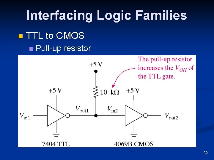
Interfacing Logic Families n TTL to CMOS n Pull-up resistor 39
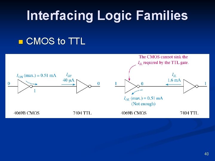
Interfacing Logic Families n CMOS to TTL 40
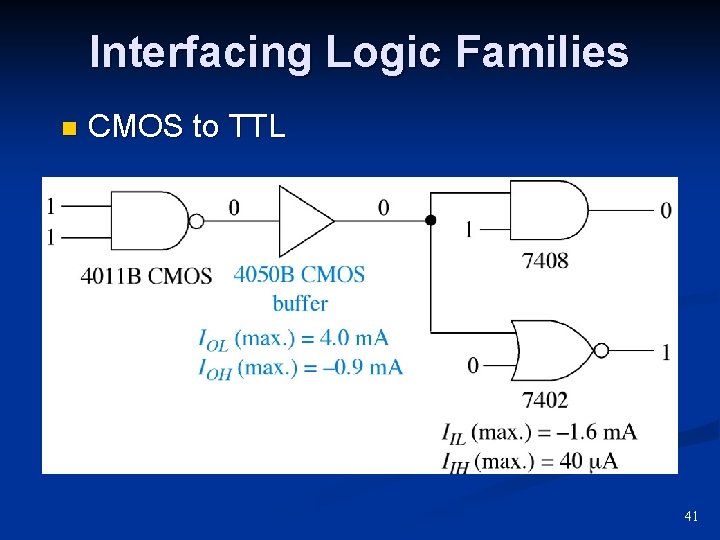
Interfacing Logic Families n CMOS to TTL 41
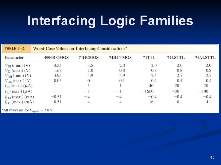
Interfacing Logic Families 42
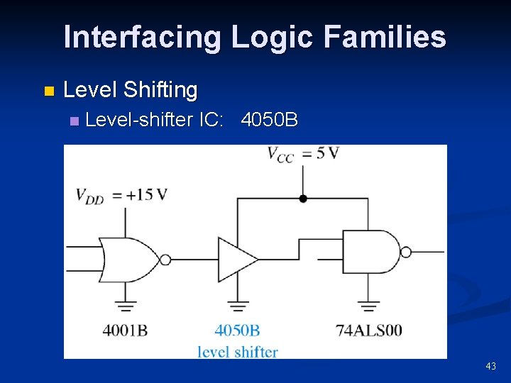
Interfacing Logic Families n Level Shifting n Level-shifter IC: 4050 B 43
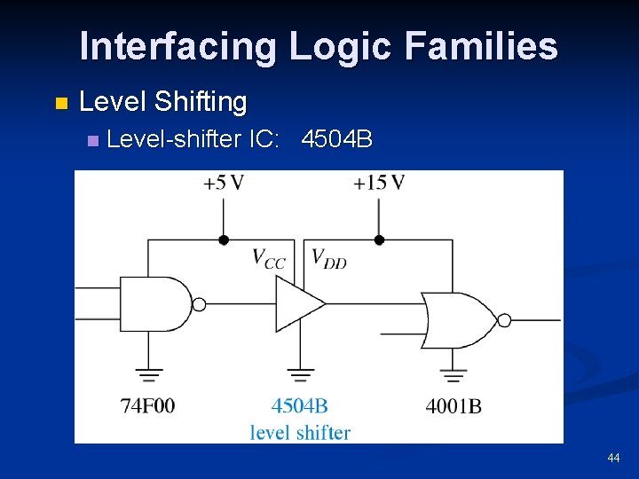
Interfacing Logic Families n Level Shifting n Level-shifter IC: 4504 B 44
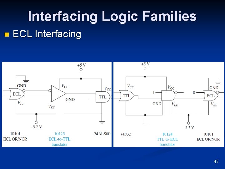
Interfacing Logic Families n ECL Interfacing 45
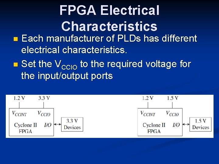
FPGA Electrical Characteristics Each manufacturer of PLDs has different electrical characteristics. n Set the VCCIO to the required voltage for the input/output ports n
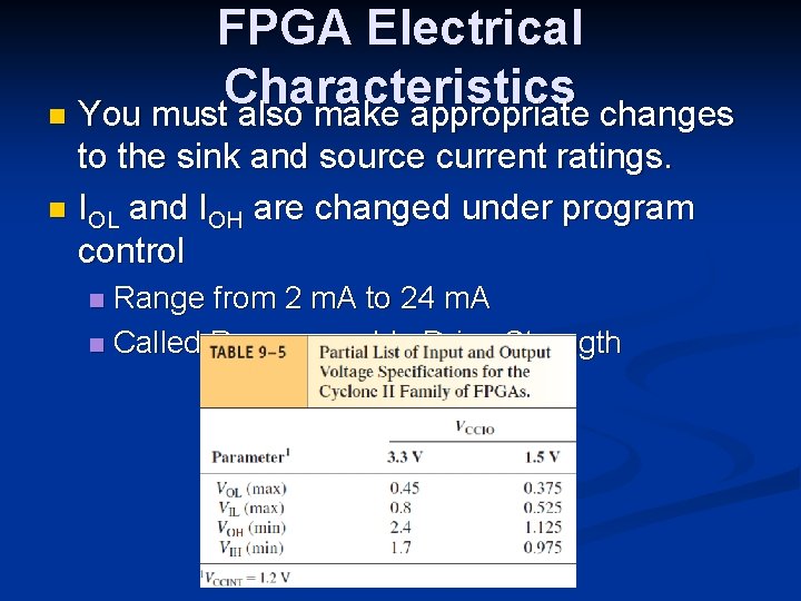
FPGA Electrical Characteristics n You must also make appropriate changes to the sink and source current ratings. n IOL and IOH are changed under program control Range from 2 m. A to 24 m. A n Called Programmable Drive Strength n
Summary There are three stages of internal circuitry in a TTL IC: input, control, and output. n The input current to an IC gate is a constant value specified by the manufacturer. n The output current of an IC gate depends on the size of the load connected to it. Its value cannot exceed the maximum rating of the chip, IOL or IOH. n 47
Summary The HIGH- and LOW-level output voltages of the standard TTL family are not 5 V and 0 V but typically are 3. 4 V and 0. 2 V. n The propagation delay is the length of time that it takes for the output of a gate to respond to a stimulus at its input. n The rise and fall times of a pulse describe how long it takes for the voltage to travel between its 10% and 90% levels. n 48
Summary Open-collector outputs are required whenever logic outputs are connected to a common point. n Several improved TTL families are available and continue to be introduced each year providing decreased power consumption and decreased propagation delay. n 49
Summary n The CMOS family uses complementary metal oxide semiconductor transistors instead of the bipolar transistors used in TTL ICs. Traditionally, the CMOS family consumed less power but was slower than TTL. However, recent advances in both technologies have narrowed the differences. 50
Summary n The Bi. CMOS family combines the best characteristics of bipolar technology and CMOS technology to provide logic functions that are optimized for the highspeed, low-power characteristics required in microprocessor systems. 51
Summary Emitter-coupled logic (ECL) provides the highest-speed ICs. Its drawback is its very high power consumption. n A figure of merit of IC families is the product of their propagation delay and power consumption, called the speedpower product (the lower, the better). n 52
Summary n When interfacing logic families, several considerations must be made. The output voltage level of one family must be high and low enough to meet the input requirements of the receiving family. Also, the output current capability of the driving gate must be high enough for the input draw of the receiving gate or gates. 53