Chapter 3 Boolean Algebra and Digital Logic Chapter
Chapter 3 Boolean Algebra and Digital Logic
Chapter 3 Objectives • Understand the relationship between Boolean logic and digital computer circuits. • Learn how to design simple logic circuits. • Understand how digital circuits work together to form complex computer systems. 2
3. 1 Introduction • In the latter part of the nineteenth century, George Boole incensed philosophers and mathematicians alike when he suggested that logical thought could be represented through mathematical equations. – How dare anyone suggest that human thought could be encapsulated and manipulated like an algebraic formula? • Computers, as we know them today, are implementations of Boole’s Laws of Thought. – John Atanasoff and Claude Shannon were among the first to see this connection. 3
3. 2 Boolean Algebra • Boolean algebra is a mathematical system for the manipulation of variables that can have one of two values. – In formal logic, these values are “true” and “false. ” – In digital systems, these values are “on” and “off, ” 1 and 0, or “high” and “low. ” • Boolean expressions are created by performing operations on Boolean variables. – Common Boolean operators include AND, OR, and NOT. 4
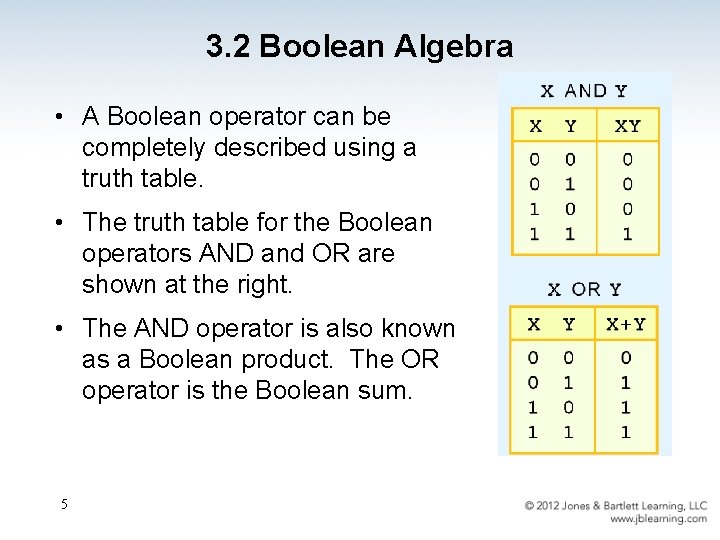
3. 2 Boolean Algebra • A Boolean operator can be completely described using a truth table. • The truth table for the Boolean operators AND and OR are shown at the right. • The AND operator is also known as a Boolean product. The OR operator is the Boolean sum. 5
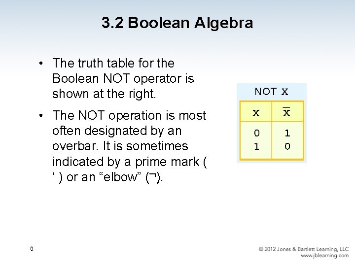
3. 2 Boolean Algebra • The truth table for the Boolean NOT operator is shown at the right. • The NOT operation is most often designated by an overbar. It is sometimes indicated by a prime mark ( ‘ ) or an “elbow” ( ). 6
3. 2 Boolean Algebra • A Boolean function has: At least one Boolean variable, • At least one Boolean operator, and • At least one input from the set {0, 1}. • • It produces an output that is also a member of the set {0, 1}. Now you know why the binary numbering system is so handy in digital systems. 7
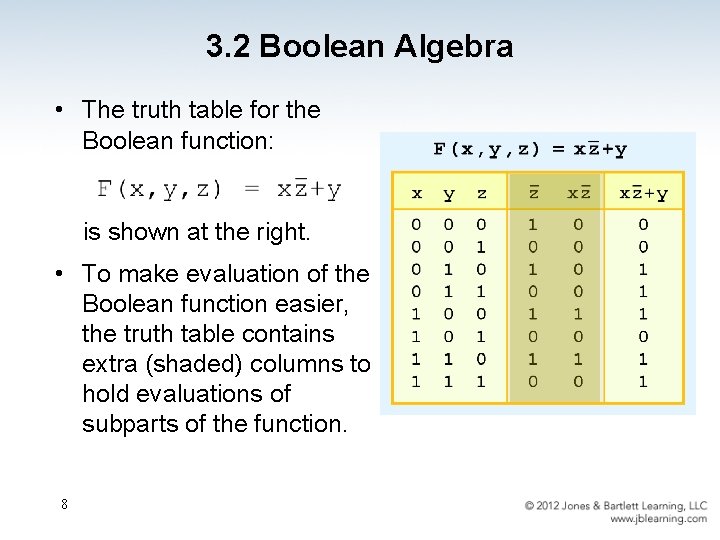
3. 2 Boolean Algebra • The truth table for the Boolean function: is shown at the right. • To make evaluation of the Boolean function easier, the truth table contains extra (shaded) columns to hold evaluations of subparts of the function. 8
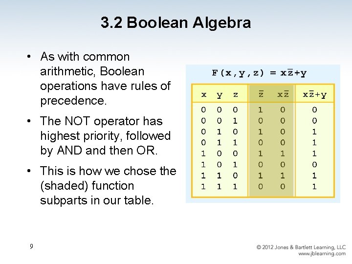
3. 2 Boolean Algebra • As with common arithmetic, Boolean operations have rules of precedence. • The NOT operator has highest priority, followed by AND and then OR. • This is how we chose the (shaded) function subparts in our table. 9
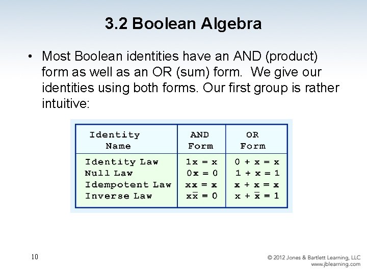
3. 2 Boolean Algebra • Most Boolean identities have an AND (product) form as well as an OR (sum) form. We give our identities using both forms. Our first group is rather intuitive: 10
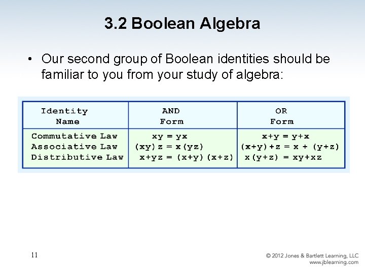
3. 2 Boolean Algebra • Our second group of Boolean identities should be familiar to you from your study of algebra: 11
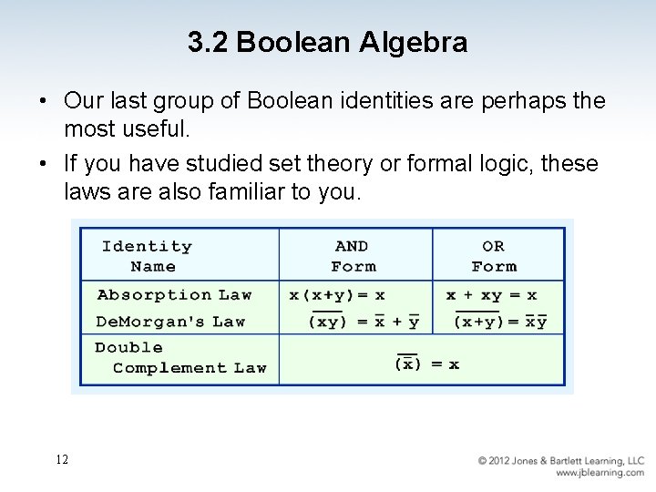
3. 2 Boolean Algebra • Our last group of Boolean identities are perhaps the most useful. • If you have studied set theory or formal logic, these laws are also familiar to you. 12
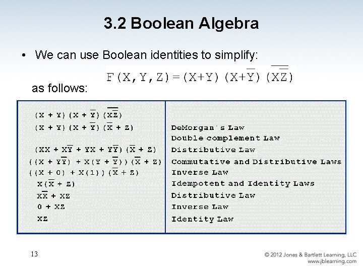
3. 2 Boolean Algebra • We can use Boolean identities to simplify: as follows: 13
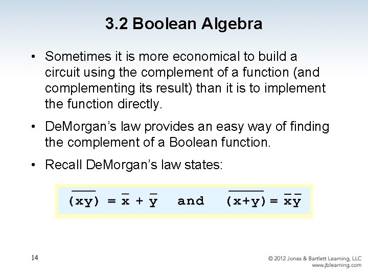
3. 2 Boolean Algebra • Sometimes it is more economical to build a circuit using the complement of a function (and complementing its result) than it is to implement the function directly. • De. Morgan’s law provides an easy way of finding the complement of a Boolean function. • Recall De. Morgan’s law states: 14
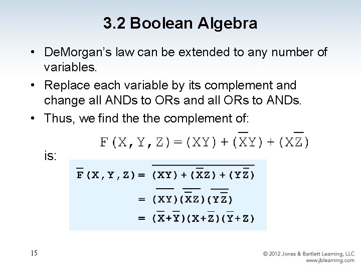
3. 2 Boolean Algebra • De. Morgan’s law can be extended to any number of variables. • Replace each variable by its complement and change all ANDs to ORs and all ORs to ANDs. • Thus, we find the complement of: is: 15
3. 2 Boolean Algebra • Through our exercises in simplifying Boolean expressions, we see that there are numerous ways of stating the same Boolean expression. – These “synonymous” forms are logically equivalent. – Logically equivalent expressions have identical truth tables. • In order to eliminate as much confusion as possible, designers express Boolean functions in standardized or canonical form. 16
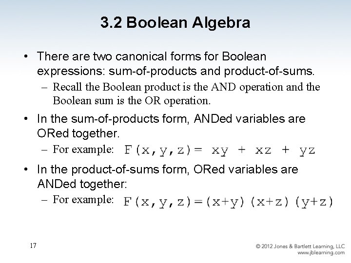
3. 2 Boolean Algebra • There are two canonical forms for Boolean expressions: sum-of-products and product-of-sums. – Recall the Boolean product is the AND operation and the Boolean sum is the OR operation. • In the sum-of-products form, ANDed variables are ORed together. – For example: • In the product-of-sums form, ORed variables are ANDed together: – For example: 17
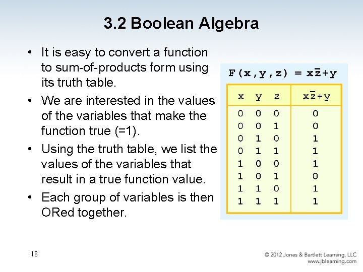
3. 2 Boolean Algebra • It is easy to convert a function to sum-of-products form using its truth table. • We are interested in the values of the variables that make the function true (=1). • Using the truth table, we list the values of the variables that result in a true function value. • Each group of variables is then ORed together. 18
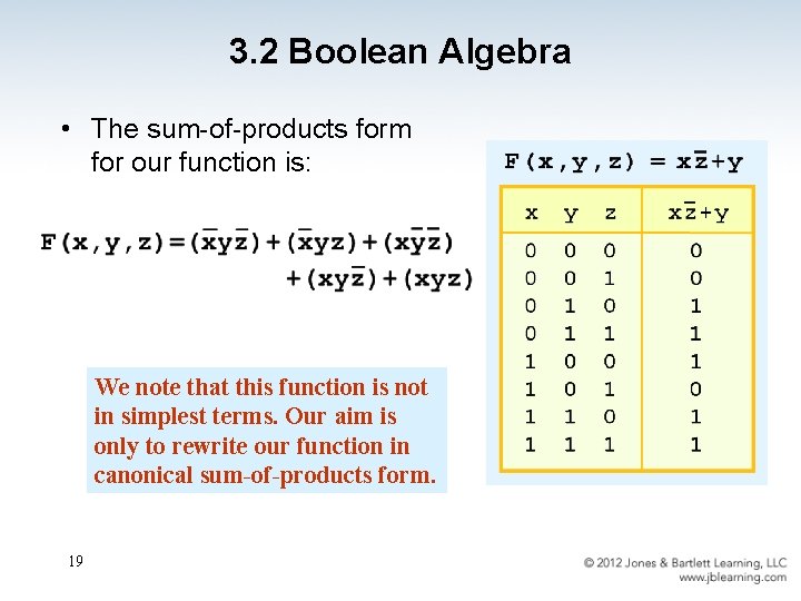
3. 2 Boolean Algebra • The sum-of-products form for our function is: We note that this function is not in simplest terms. Our aim is only to rewrite our function in canonical sum-of-products form. 19
3. 3 Logic Gates • We have looked at Boolean functions in abstract terms. • In this section, we see that Boolean functions are implemented in digital computer circuits called gates. • A gate is an electronic device that produces a result based on two or more input values. – In reality, gates consist of one to six transistors, but digital designers think of them as a single unit. – Integrated circuits contain collections of gates suited to a particular purpose. 20
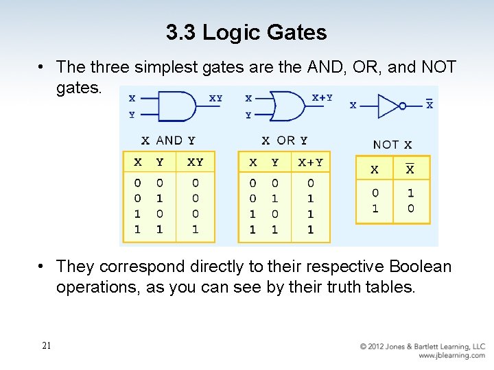
3. 3 Logic Gates • The three simplest gates are the AND, OR, and NOT gates. • They correspond directly to their respective Boolean operations, as you can see by their truth tables. 21
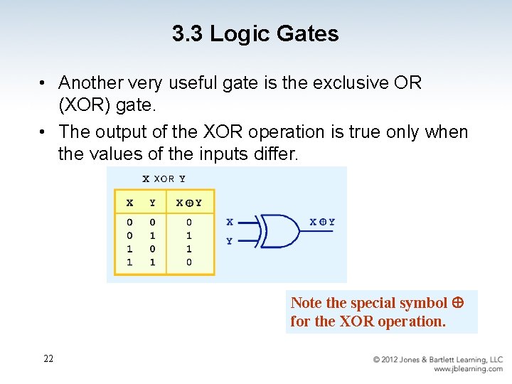
3. 3 Logic Gates • Another very useful gate is the exclusive OR (XOR) gate. • The output of the XOR operation is true only when the values of the inputs differ. Note the special symbol for the XOR operation. 22
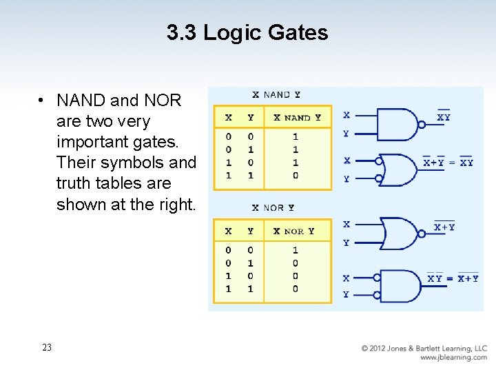
3. 3 Logic Gates • NAND and NOR are two very important gates. Their symbols and truth tables are shown at the right. 23
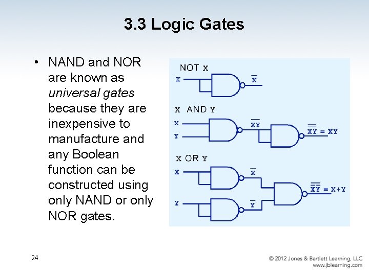
3. 3 Logic Gates • NAND and NOR are known as universal gates because they are inexpensive to manufacture and any Boolean function can be constructed using only NAND or only NOR gates. 24
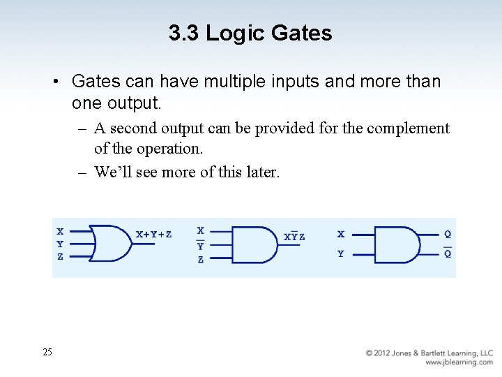
3. 3 Logic Gates • Gates can have multiple inputs and more than one output. – A second output can be provided for the complement of the operation. – We’ll see more of this later. 25
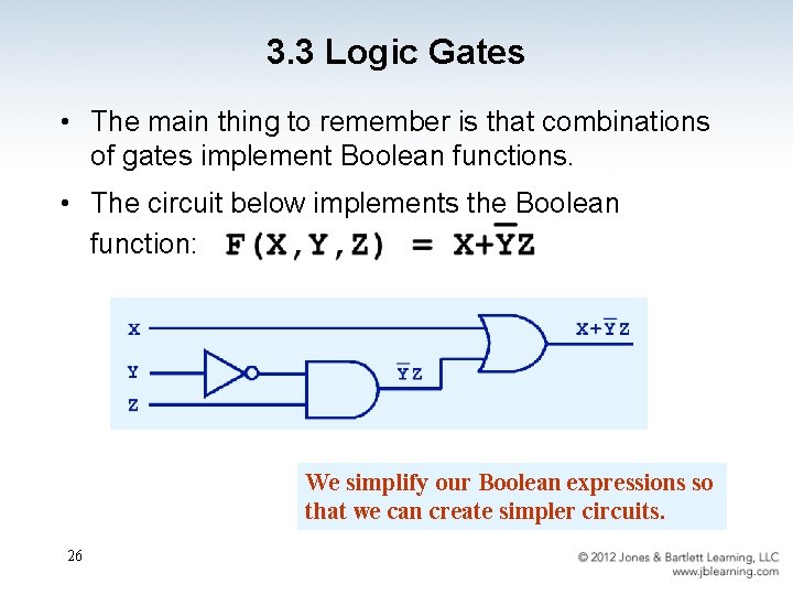
3. 3 Logic Gates • The main thing to remember is that combinations of gates implement Boolean functions. • The circuit below implements the Boolean function: We simplify our Boolean expressions so that we can create simpler circuits. 26
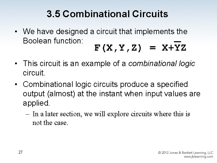
3. 5 Combinational Circuits • We have designed a circuit that implements the Boolean function: • This circuit is an example of a combinational logic circuit. • Combinational logic circuits produce a specified output (almost) at the instant when input values are applied. – In a later section, we will explore circuits where this is not the case. 27
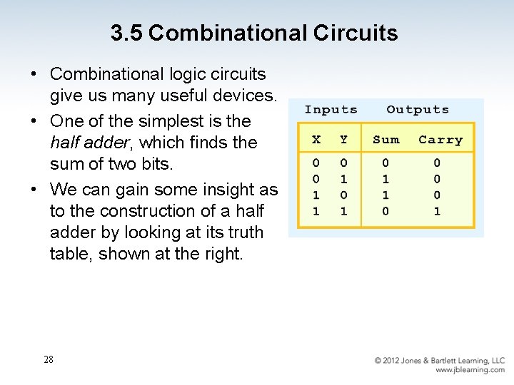
3. 5 Combinational Circuits • Combinational logic circuits give us many useful devices. • One of the simplest is the half adder, which finds the sum of two bits. • We can gain some insight as to the construction of a half adder by looking at its truth table, shown at the right. 28
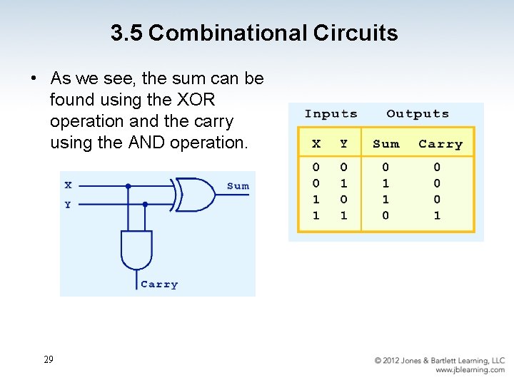
3. 5 Combinational Circuits • As we see, the sum can be found using the XOR operation and the carry using the AND operation. 29
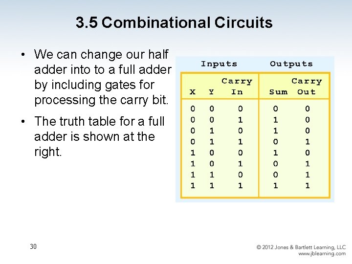
3. 5 Combinational Circuits • We can change our half adder into to a full adder by including gates for processing the carry bit. • The truth table for a full adder is shown at the right. 30
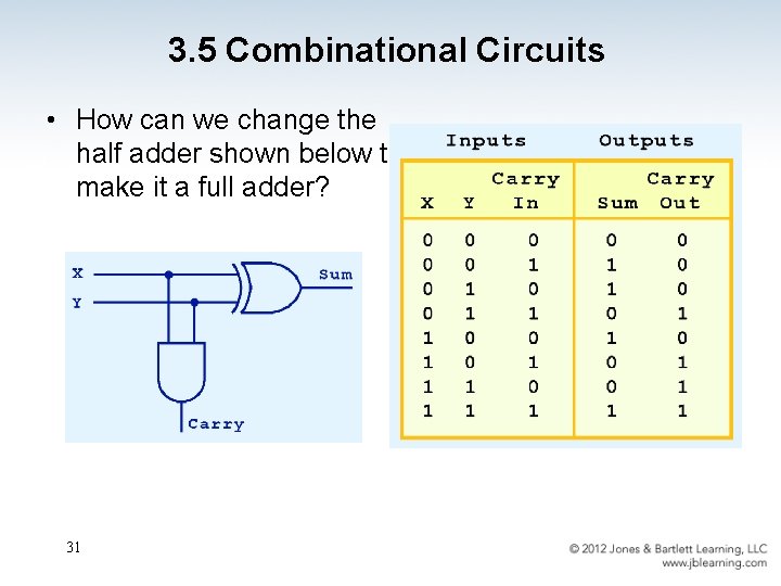
3. 5 Combinational Circuits • How can we change the half adder shown below to make it a full adder? 31
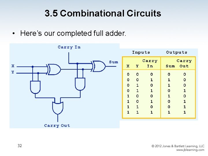
3. 5 Combinational Circuits • Here’s our completed full adder. 32
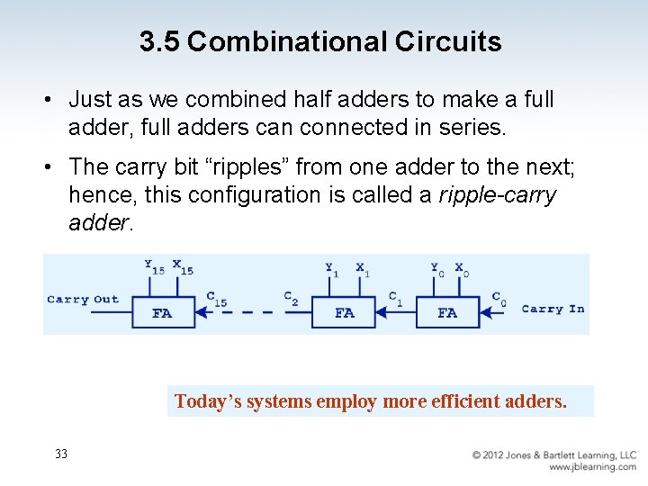
3. 5 Combinational Circuits • Just as we combined half adders to make a full adder, full adders can connected in series. • The carry bit “ripples” from one adder to the next; hence, this configuration is called a ripple-carry adder. Today’s systems employ more efficient adders. 33
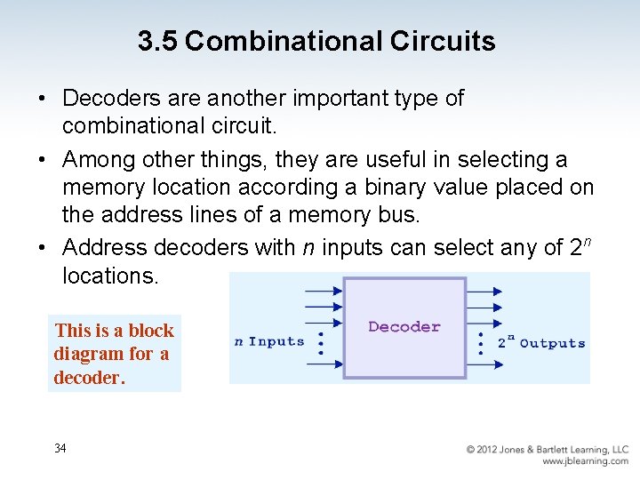
3. 5 Combinational Circuits • Decoders are another important type of combinational circuit. • Among other things, they are useful in selecting a memory location according a binary value placed on the address lines of a memory bus. • Address decoders with n inputs can select any of 2 n locations. This is a block diagram for a decoder. 34
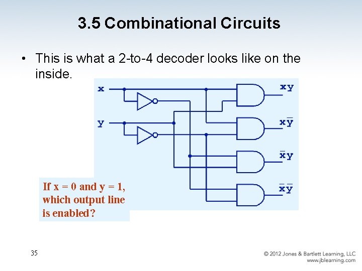
3. 5 Combinational Circuits • This is what a 2 -to-4 decoder looks like on the inside. If x = 0 and y = 1, which output line is enabled? 35
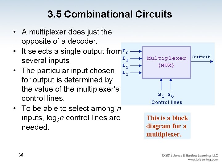
3. 5 Combinational Circuits • A multiplexer does just the opposite of a decoder. • It selects a single output from several inputs. • The particular input chosen for output is determined by the value of the multiplexer’s control lines. • To be able to select among n inputs, log 2 n control lines are needed. 36 This is a block diagram for a multiplexer.

3. 5 Combinational Circuits • This is what a 4 -to-1 multiplexer looks like on the inside. If S 0 = 1 and S 1 = 0, which input is transferred to the output? 37
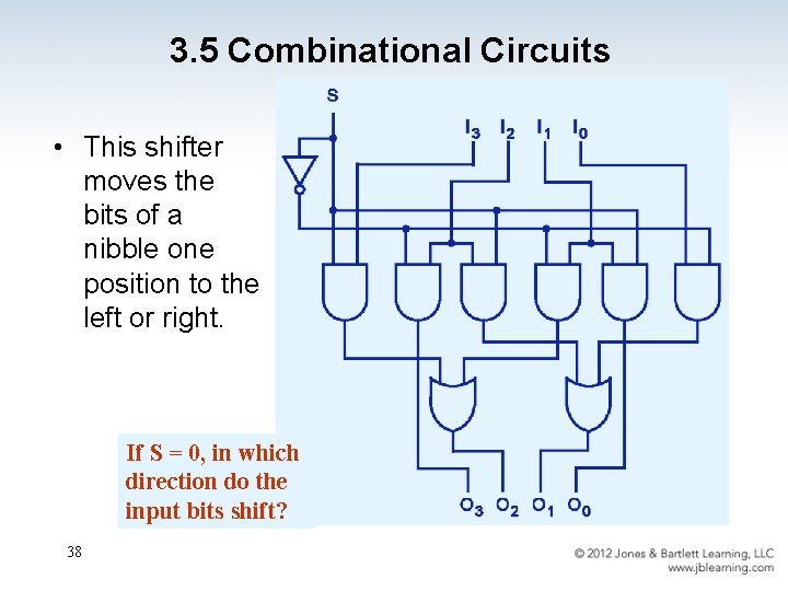
3. 5 Combinational Circuits • This shifter moves the bits of a nibble one position to the left or right. If S = 0, in which direction do the input bits shift? 38
3. 6 Sequential Circuits • Combinational logic circuits are perfect for situations when we require the immediate application of a Boolean function to a set of inputs. • There are other times, however, when we need a circuit to change its value with consideration to its current state as well as its inputs. – These circuits have to “remember” their current state. • Sequential logic circuits provide this functionality for us. 39
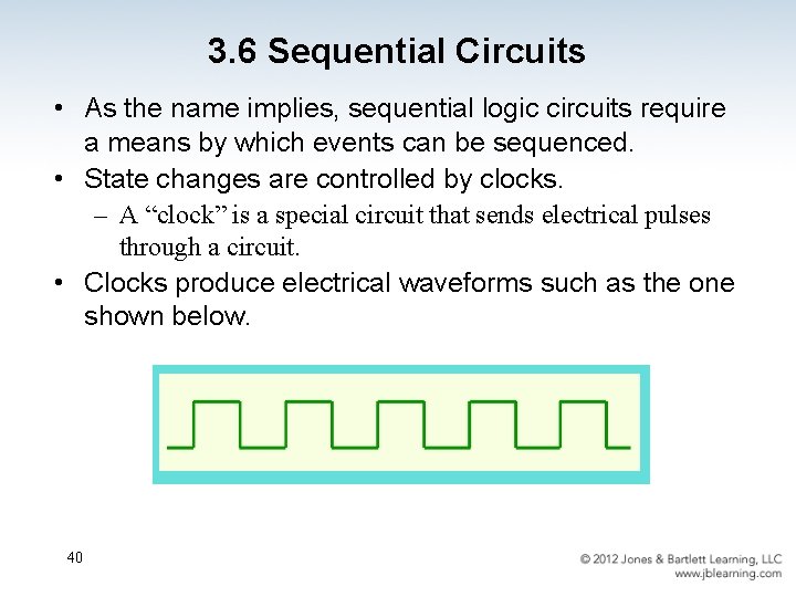
3. 6 Sequential Circuits • As the name implies, sequential logic circuits require a means by which events can be sequenced. • State changes are controlled by clocks. – A “clock” is a special circuit that sends electrical pulses through a circuit. • Clocks produce electrical waveforms such as the one shown below. 40
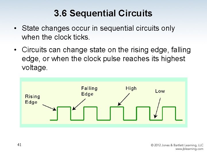
3. 6 Sequential Circuits • State changes occur in sequential circuits only when the clock ticks. • Circuits can change state on the rising edge, falling edge, or when the clock pulse reaches its highest voltage. 41
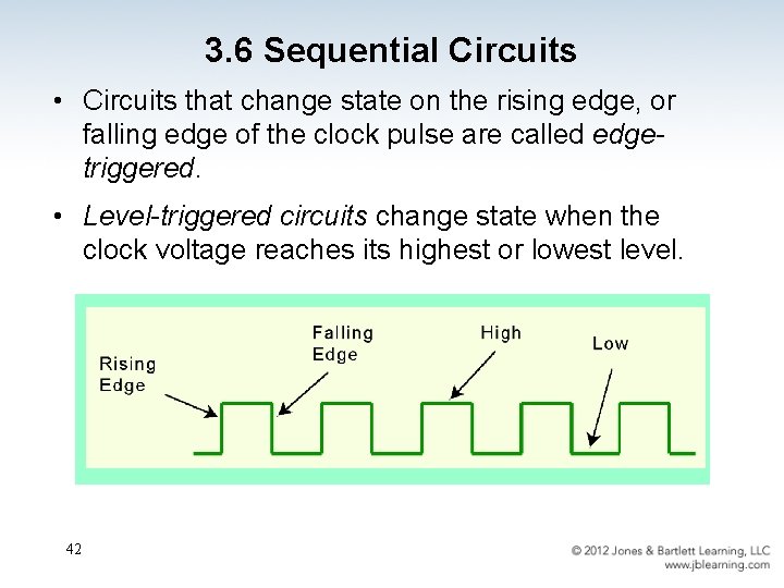
3. 6 Sequential Circuits • Circuits that change state on the rising edge, or falling edge of the clock pulse are called edgetriggered. • Level-triggered circuits change state when the clock voltage reaches its highest or lowest level. 42
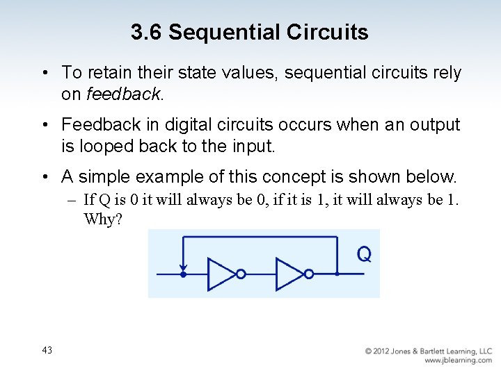
3. 6 Sequential Circuits • To retain their state values, sequential circuits rely on feedback. • Feedback in digital circuits occurs when an output is looped back to the input. • A simple example of this concept is shown below. – If Q is 0 it will always be 0, if it is 1, it will always be 1. Why? 43
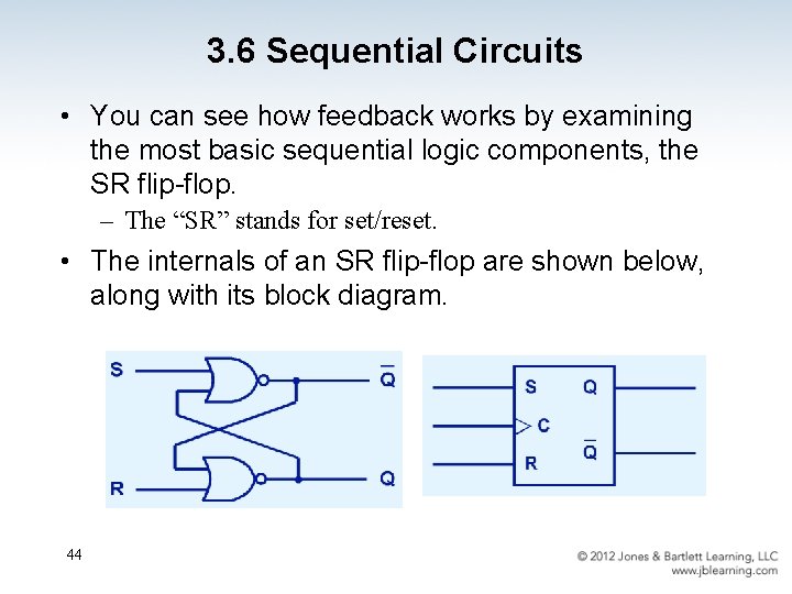
3. 6 Sequential Circuits • You can see how feedback works by examining the most basic sequential logic components, the SR flip-flop. – The “SR” stands for set/reset. • The internals of an SR flip-flop are shown below, along with its block diagram. 44
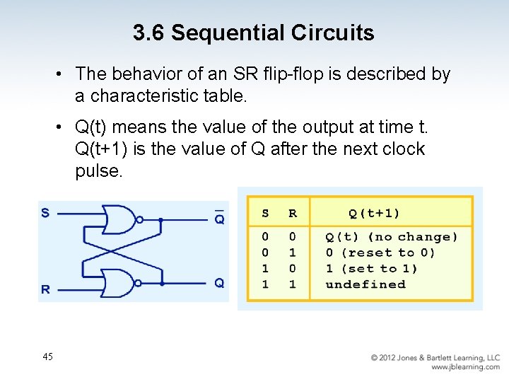
3. 6 Sequential Circuits • The behavior of an SR flip-flop is described by a characteristic table. • Q(t) means the value of the output at time t. Q(t+1) is the value of Q after the next clock pulse. 45
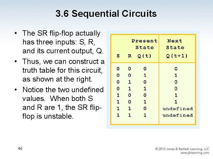
3. 6 Sequential Circuits • The SR flip-flop actually has three inputs: S, R, and its current output, Q. • Thus, we can construct a truth table for this circuit, as shown at the right. • Notice the two undefined values. When both S and R are 1, the SR flipflop is unstable. 46
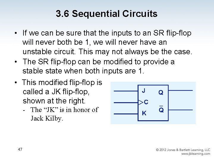
3. 6 Sequential Circuits • If we can be sure that the inputs to an SR flip-flop will never both be 1, we will never have an unstable circuit. This may not always be the case. • The SR flip-flop can be modified to provide a stable state when both inputs are 1. • This modified flip-flop is called a JK flip-flop, shown at the right. - 47 The “JK” is in honor of Jack Kilby.
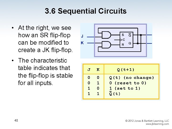
3. 6 Sequential Circuits • At the right, we see how an SR flip-flop can be modified to create a JK flip-flop. • The characteristic table indicates that the flip-flop is stable for all inputs. 48
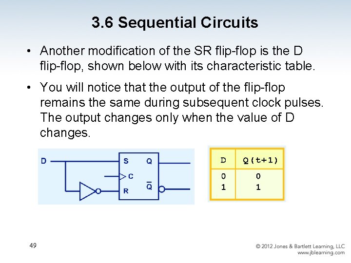
3. 6 Sequential Circuits • Another modification of the SR flip-flop is the D flip-flop, shown below with its characteristic table. • You will notice that the output of the flip-flop remains the same during subsequent clock pulses. The output changes only when the value of D changes. 49
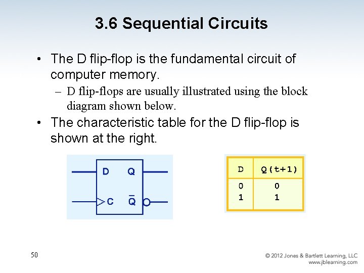
3. 6 Sequential Circuits • The D flip-flop is the fundamental circuit of computer memory. – D flip-flops are usually illustrated using the block diagram shown below. • The characteristic table for the D flip-flop is shown at the right. 50
3. 6 Sequential Circuits • The behavior of sequential circuits can be expressed using characteristic tables or finite state machines (FSMs). – FSMs consist of a set of nodes that hold the states of the machine and a set of arcs that connect the states. • Moore and Mealy machines are two types of FSMs that are equivalent. – They differ only in how they express the outputs of the machine. • Moore machines place outputs on each node, while Mealy machines present their outputs on the transitions. 51

3. 6 Sequential Circuits • The behavior of a JK flop-flop is depicted below by a Moore machine (left) and a Mealy machine (right). 52
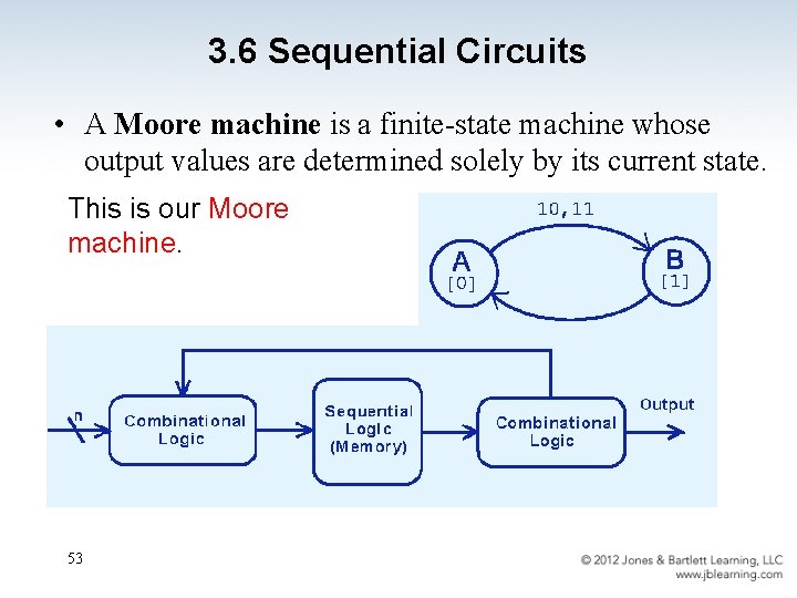
3. 6 Sequential Circuits • A Moore machine is a finite-state machine whose output values are determined solely by its current state. This is our Moore machine. 53
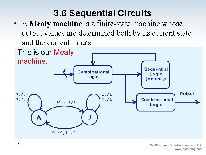
3. 6 Sequential Circuits • A Mealy machine is a finite-state machine whose output values are determined both by its current state and the current inputs. This is our Mealy machine. 54
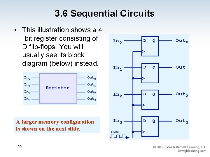
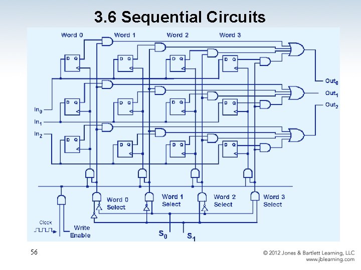
3. 6 Sequential Circuits • This illustration shows a 4 -bit register consisting of D flip-flops. You will usually see its block diagram (below) instead. A larger memory configuration is shown on the next slide. 55
3. 6 Sequential Circuits 56
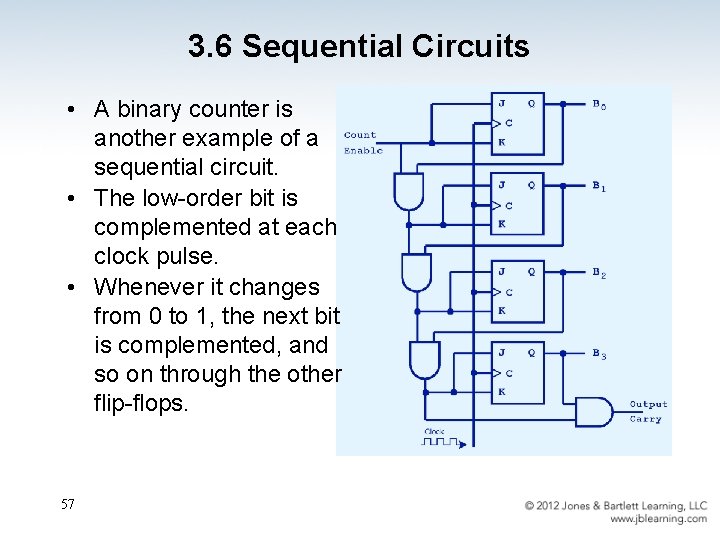
3. 6 Sequential Circuits • A binary counter is another example of a sequential circuit. • The low-order bit is complemented at each clock pulse. • Whenever it changes from 0 to 1, the next bit is complemented, and so on through the other flip-flops. 57
3. 6 Sequential Circuits 58
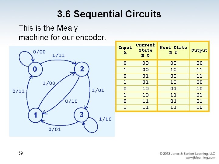
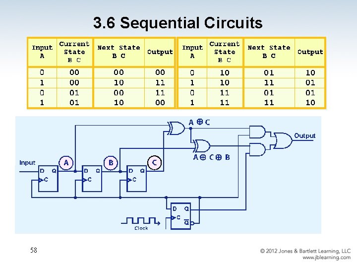
3. 6 Sequential Circuits This is the Mealy machine for our encoder. 59
Chapter 3 Conclusion • Computers are implementations of Boolean logic. • Boolean functions are completely described by truth tables. • Logic gates are small circuits that implement Boolean operators. • The basic gates are AND, OR, and NOT. – The XOR gate is very useful in parity checkers and adders. • The “universal gates” are NOR, and NAND. 60
Chapter 3 Conclusion • Computer circuits consist of combinational logic circuits and sequential logic circuits. • Combinational circuits produce outputs (almost) immediately when their inputs change. • Sequential circuits require clocks to control their changes of state. • The basic sequential circuit unit is the flip-flop: The behaviors of the SR, JK, and D flip-flops are the most important to know. 61

Chapter 3 Conclusion • The behavior of sequential circuits can be expressed using characteristic tables or through various finite state machines. • Moore and Mealy machines are two finite state machines that model high-level circuit behavior. • Algorithmic state machines are better than Moore and Mealy machines at expressing timing and complex signal interactions. • Examples of sequential circuits include memory, counters, and Viterbi encoders and decoders. 62
- Slides: 62