IC Logic Families WenHung Liao Ph D Digital

- Slides: 51
IC Logic Families Wen-Hung Liao, Ph. D
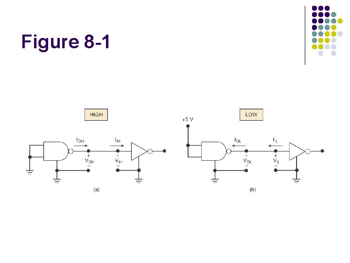
Digital IC Terminology l Voltage Parameters: l l VIH(min): high-level input voltage, the minimum voltage level required for a logic 1 at an input. VIL(max): low-level input voltage VOH(min): high-level output voltage VOL(max): low-level output voltage
Current Parameters l IIH(min): l l l high-level input current, the current that flows into an input when a specified highlevel voltage is applied to that input. IIL(max): low-level input current IOH(min): high-level output current IOL(max): low-level output current
Figure 8 -1
Fan-Out l l l The maximum number of standard logic inputs that an output can drive reliably. Also known as the loading factor. Related to the current parameters (both in high and low states. )
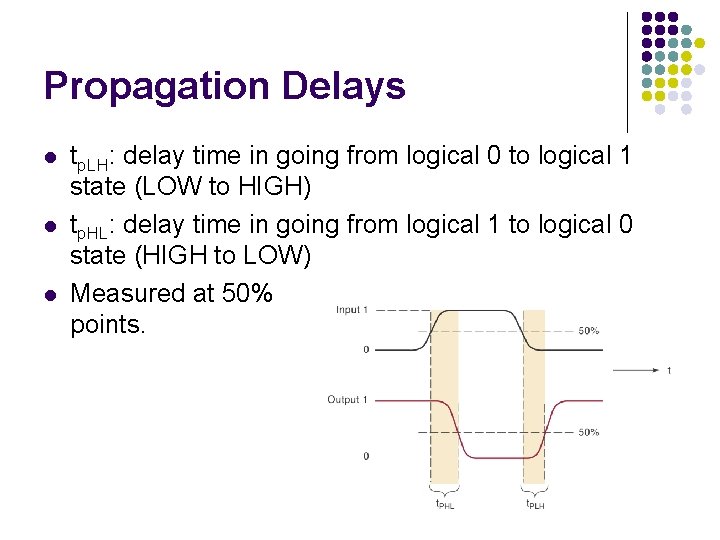
Propagation Delays l l l tp. LH: delay time in going from logical 0 to logical 1 state (LOW to HIGH) tp. HL: delay time in going from logical 1 to logical 0 state (HIGH to LOW) Measured at 50% points.
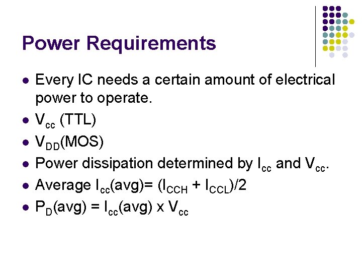
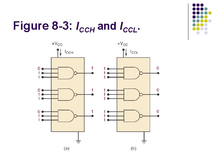
Power Requirements l l l Every IC needs a certain amount of electrical power to operate. Vcc (TTL) VDD(MOS) Power dissipation determined by Icc and Vcc. Average Icc(avg)= (ICCH + ICCL)/2 PD(avg) = Icc(avg) x Vcc
Figure 8 -3: ICCH and ICCL.
Speed-Power Product l Desirable properties: l l l Short propagation delays (high speed) Low power dissipation Speed-power product measures the combined effect.
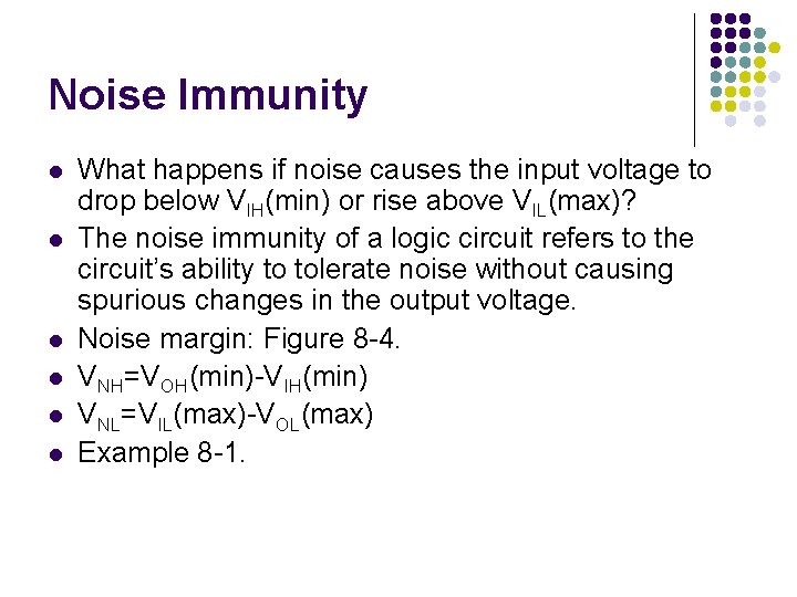
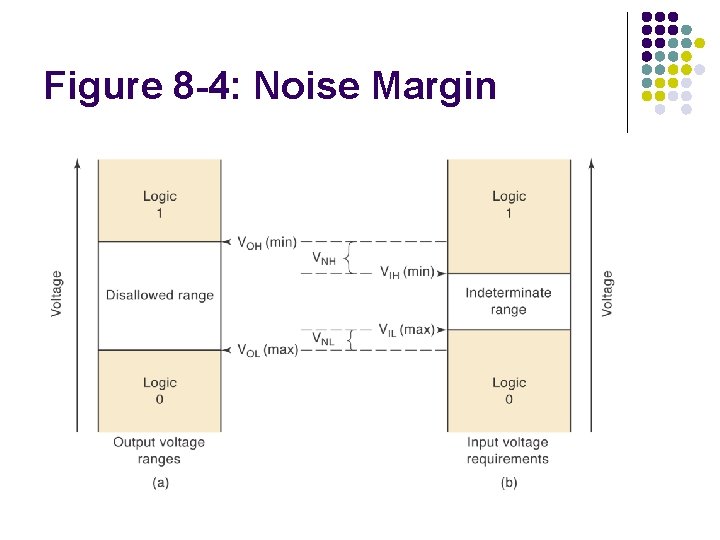
Noise Immunity l l l What happens if noise causes the input voltage to drop below VIH(min) or rise above VIL(max)? The noise immunity of a logic circuit refers to the circuit’s ability to tolerate noise without causing spurious changes in the output voltage. Noise margin: Figure 8 -4. VNH=VOH(min)-VIH(min) VNL=VIL(max)-VOL(max) Example 8 -1.
Figure 8 -4: Noise Margin
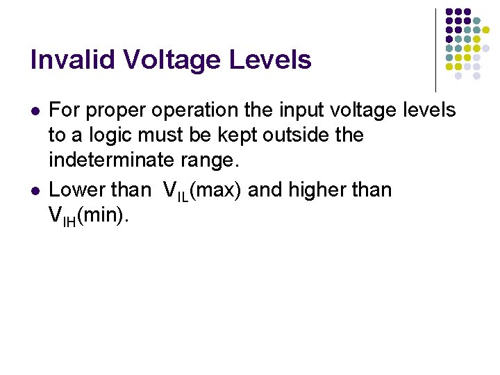
Invalid Voltage Levels l l For properation the input voltage levels to a logic must be kept outside the indeterminate range. Lower than VIL(max) and higher than VIH(min).
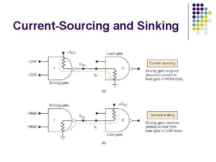
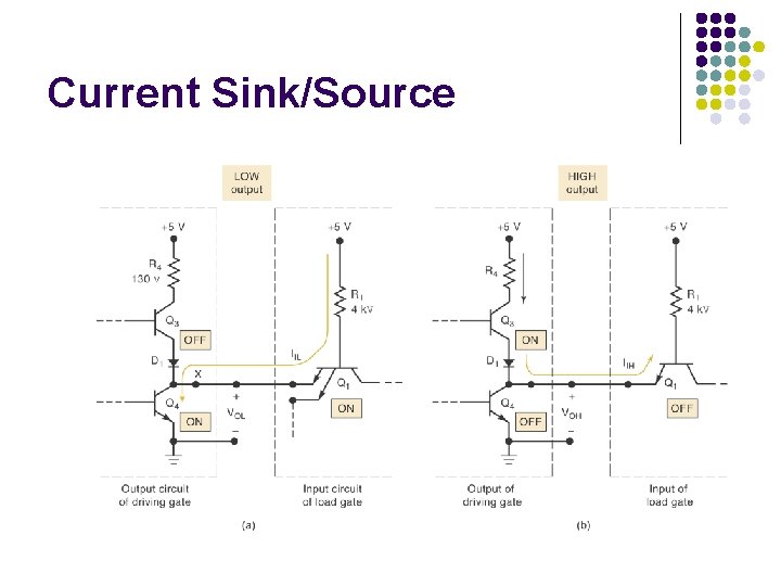
Current-Sourcing and Sinking
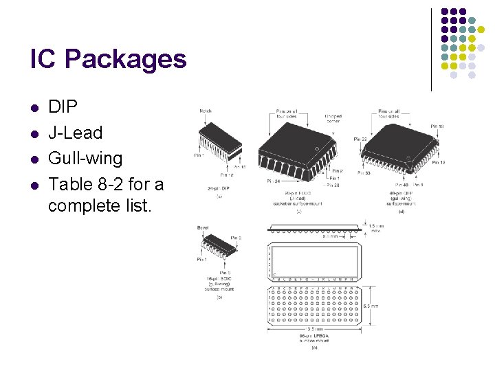
IC Packages l l DIP J-Lead Gull-wing Table 8 -2 for a complete list.
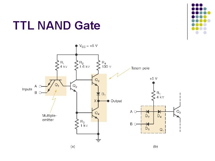
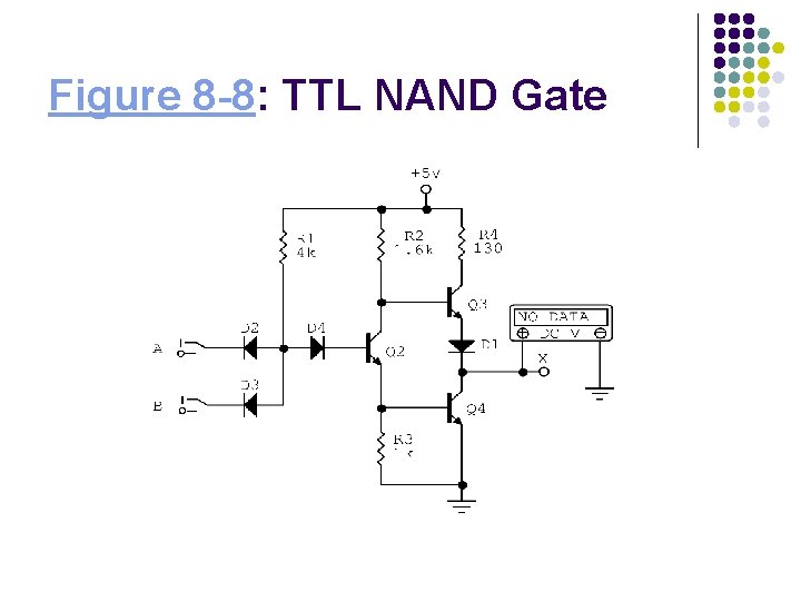
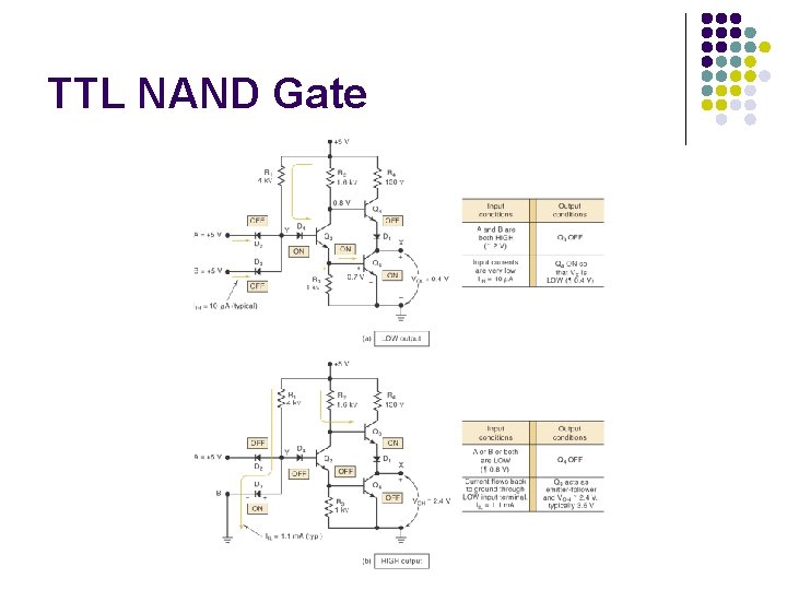
The TTL Logic Family l l Transistor-transistor logic Figure 8 -7: NAND gate. Circuit operation: LOW state, current-sinking Circuit operation: HIGH state, currentsourcing.
TTL NAND Gate
Figure 8 -8: TTL NAND Gate
TTL NAND Gate
Current Sink/Source
TTL NOR Gate Circuit
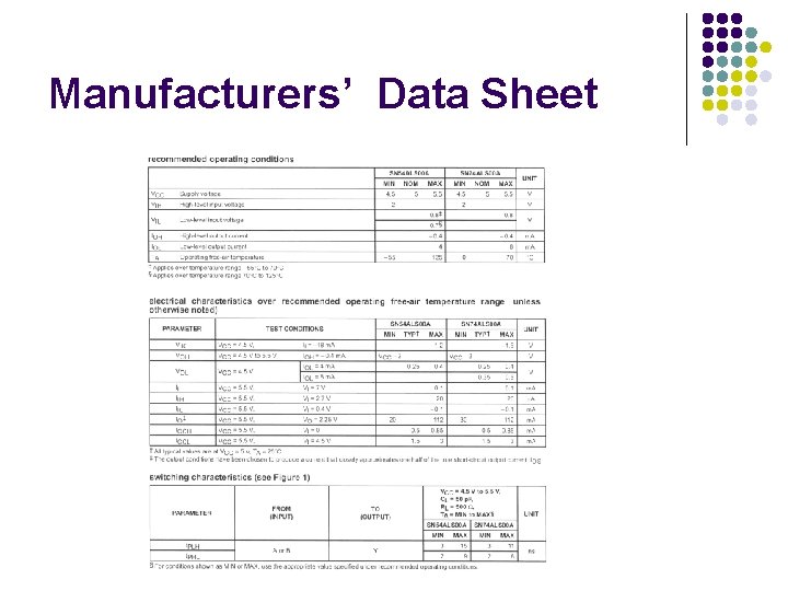
Standard TTL Characteristics l l TI introduced first line of standard TTL: 54/74 series (1964) Manufacturers’ data sheets (Figure 8 -11) l l l l Supply voltage and temperature range Voltage levels Maximum voltage ratings Power dissipation Propagation delays Fan-out Example 8 -2: maximum average power dissipation and maximum average propagation delay.
Manufacturers’ Data Sheet
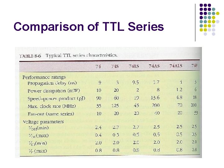
Improved TTL Series l l l 74 Series Schottky TTL, 74 S Series: higher speed Low-Power Schottky TTL, 74 LS series Advanced Schottky TTL, 74 AS Series Advanced Low-Power Schottky TTL, 74 ALS Series 74 F-Fast TTL
Comparison of TTL Series
Examples l l Example 8 -3: Noise margin of 74 and 74 LS Example 8 -4: TTL series with max number of fan-out
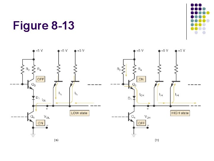
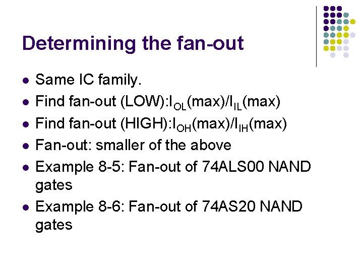
TTL Loading and Fan-Out l l l Figure 8 -13: currents when a TTL output is driving several inputs. TTL output has a limit, IOL(max), on how much current it can sink in the LOW state. It also has a limit, IOH(max), on how much current it can source in the HIGH state.
Figure 8 -13
Determining the fan-out l l l Same IC family. Find fan-out (LOW): IOL(max)/IIL(max) Find fan-out (HIGH): IOH(max)/IIH(max) Fan-out: smaller of the above Example 8 -5: Fan-out of 74 ALS 00 NAND gates Example 8 -6: Fan-out of 74 AS 20 NAND gates
Determining the fan-out l l Different IC families Step 1: add up the IIH for all inputs connected to an output. The sum must be less than the output’s IOH specification. Step 2: add up the IIL for all inputs connected to an output. The sum must be less than the output’s IOL specification. Examples 8 -7 to 8 -9.
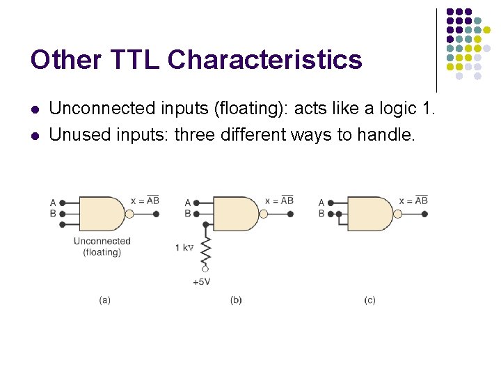
Other TTL Characteristics l l Unconnected inputs (floating): acts like a logic 1. Unused inputs: three different ways to handle.
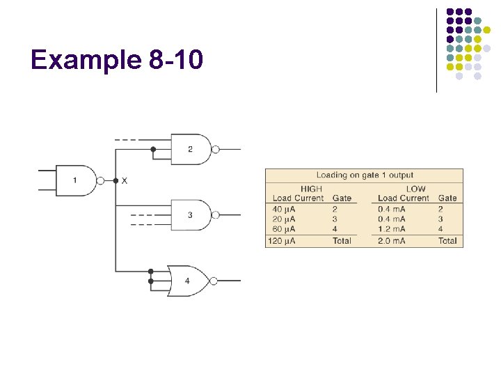
Other TTL Characteristics (cont’d) l Tie-together inputs: common input generally represent a load that is the sum of the load current rating of each individual input. Exception: for AND and NAND gates, the LOW state input load will be the same as a single input no matter how many inputs are tied together.
Example 8 -10
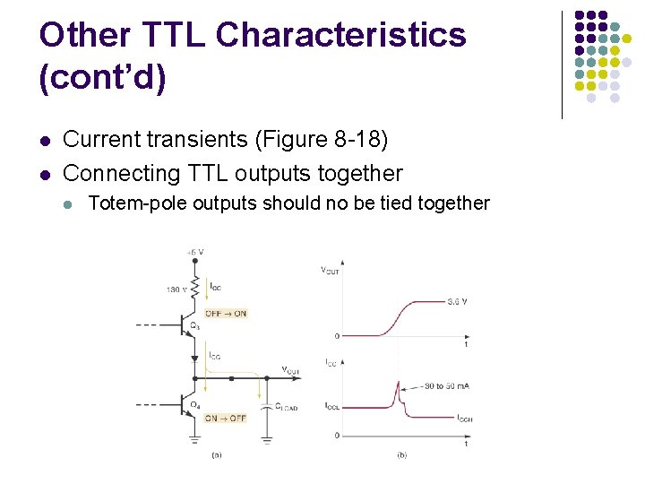
Other TTL Characteristics (cont’d) l l Current transients (Figure 8 -18) Connecting TTL outputs together l Totem-pole outputs should no be tied together
MOS Digital ICs l l l MOS: metal-oxide-semiconductor MOSFET: MOS field-effect transistors. The Good: l l l Simple Inexpensive to fabricate Small Consumes little power The bad: l l Static-electricity damage Slower than TTL
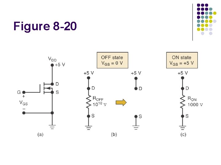
The MOSFET l l P-MOS: P-channel MOS N-MOS: N-channel MOS, fastest CMOS: complementary MOS, higher speed, lower power dissipation. Figure 8 -20: how N-channel MOSFET works: l l VGS=0 V OFF State, Roff= 1010 ohms VGS=5 V ON State, Ron=1000 ohms
Figure 8 -20
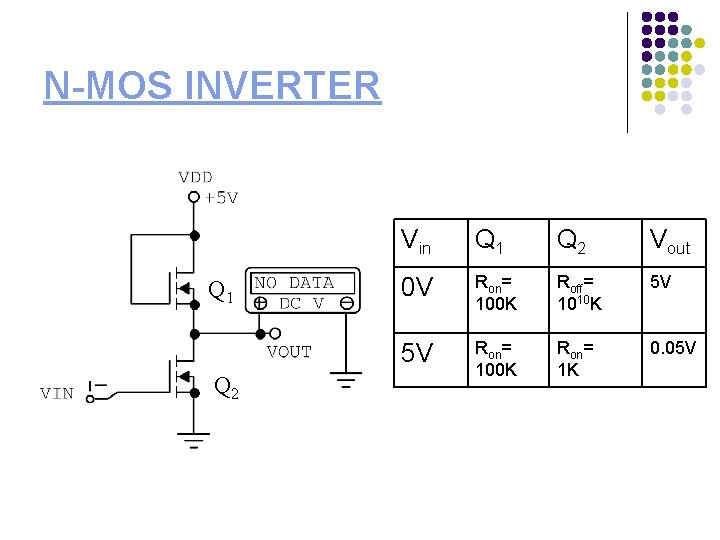
N-MOS INVERTER Q 1 Q 2 Vin Q 1 Q 2 Vout 0 V Ron= 100 K Roff= 1010 K 5 V 5 V Ron= 100 K Ron= 1 K 0. 05 V
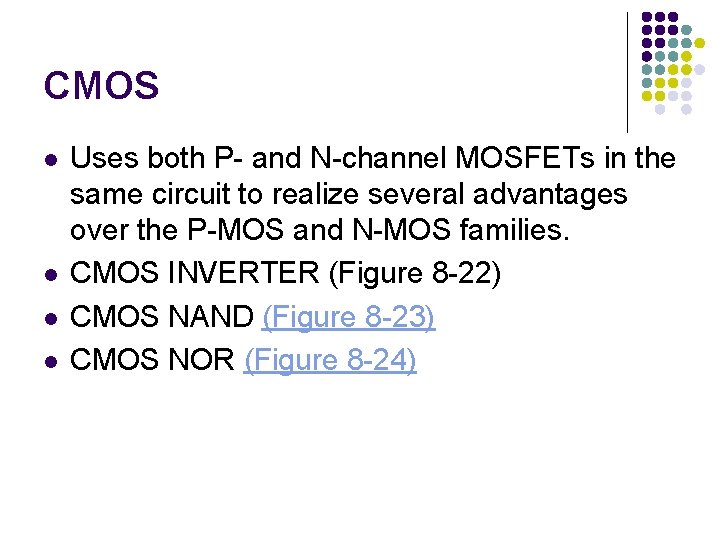
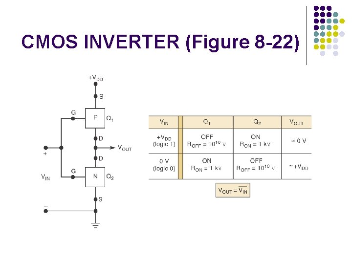
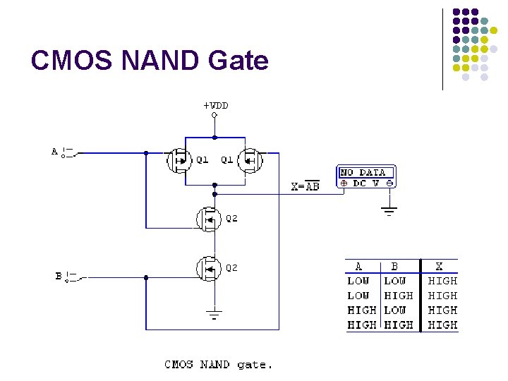
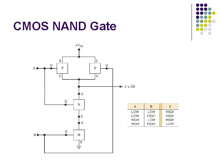
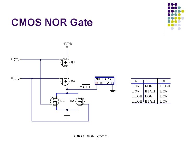
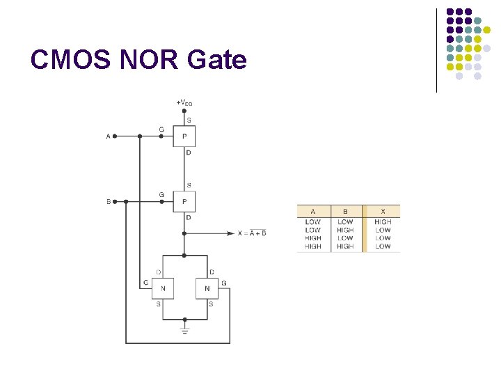
CMOS l l Uses both P- and N-channel MOSFETs in the same circuit to realize several advantages over the P-MOS and N-MOS families. CMOS INVERTER (Figure 8 -22) CMOS NAND (Figure 8 -23) CMOS NOR (Figure 8 -24)
CMOS INVERTER (Figure 8 -22)
CMOS NAND Gate
CMOS NAND Gate
CMOS NOR Gate
CMOS NOR Gate
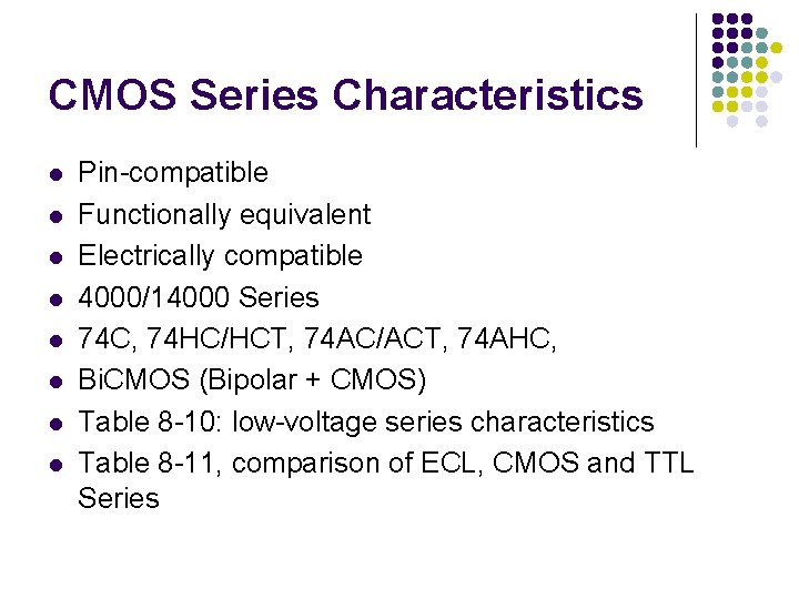
CMOS Series Characteristics l l l l Pin-compatible Functionally equivalent Electrically compatible 4000/14000 Series 74 C, 74 HC/HCT, 74 AC/ACT, 74 AHC, Bi. CMOS (Bipolar + CMOS) Table 8 -10: low-voltage series characteristics Table 8 -11, comparison of ECL, CMOS and TTL Series
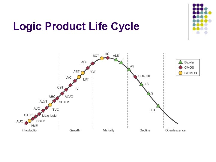
Logic Product Life Cycle
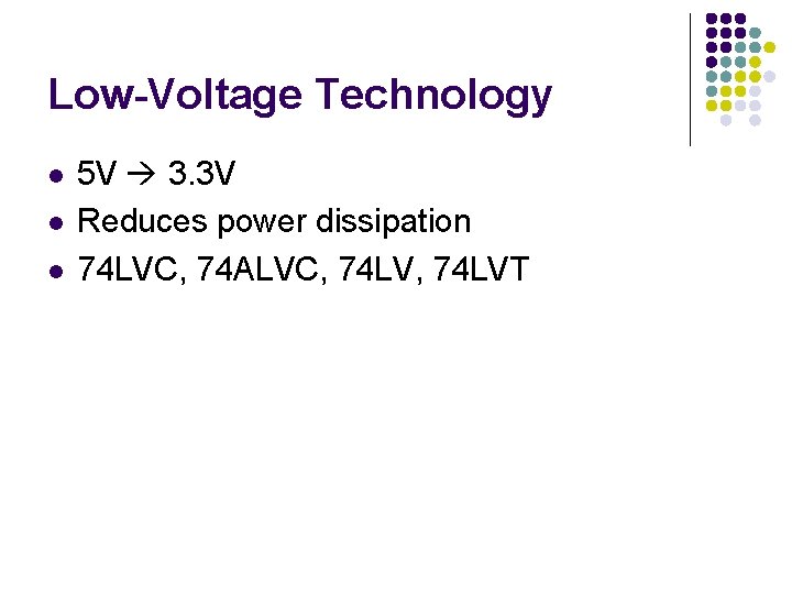
Low-Voltage Technology l l l 5 V 3. 3 V Reduces power dissipation 74 LVC, 74 ALVC, 74 LVT
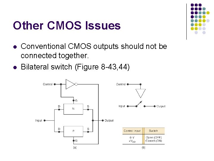
Other CMOS Issues l l Conventional CMOS outputs should not be connected together. Bilateral switch (Figure 8 -43, 44)
IC Interfacing l l Connecting the output(s) of one circuit to the input(s) of another circuit that has different electrical characteristics. Occurs often in complex digital systems, where designers utilize different logic families for different parts of system. TTL driving CMOS driving TTL
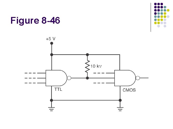
TTL driving CMOS l l l No problem with the current requirements (See Table 8 -12) VOH(min) of TTL is low compared to VIH(min) of some CMOS series (Table 8 -9), use pull-up resistor to raise TTL output voltage (Figure 8 -46) TTL driving high-voltage CMOS (VDD of CMOS is greater than 5 V) l l Use 7407 buffer Use voltage level-translator (such as 4504 B)
Figure 8 -46
CMOS driving TTL l l HIGH state: Table 8 -9 and 8 -12 indicate no special consideration the HIGH state. LOW state: depends on the series used.