40090 04 Introduction to Digital Logic Design Digital
 Introduction to Digital Logic Design 강의 소개")

 저자: Morris Mano 출판사:")


? S (set) Q 0/0 A")


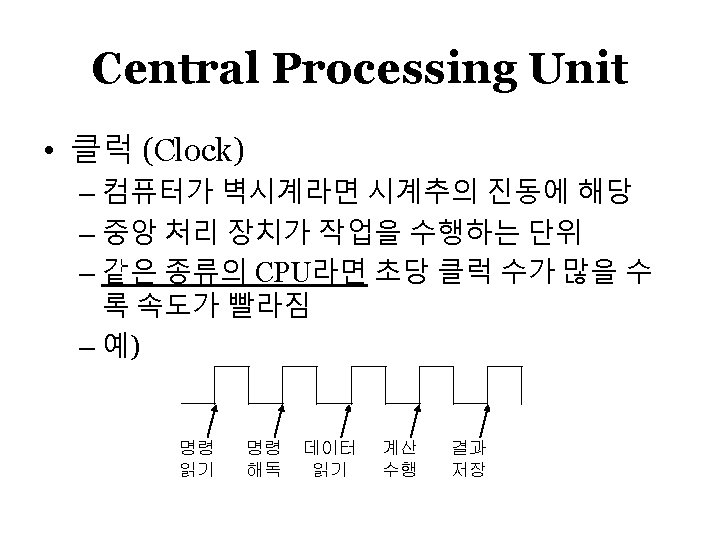
 Binary Adders • Addition of 3 binary inputs, 'Full Adder' Logic Diagram of")

 – SR f/f – JK f/f – D")
 Y 1 D C R Z X Clock Reset Y 2")


 – 주로 읽을 수만 있는 장치 –")

- Slides: 22
디지털논리설계 (40090 -04) Introduction to Digital Logic Design 강의 소개
부교재 • • 제목: Digital Design (5 th Ed. ) 저자: Morris Mano 출판사: Pearson 출판년도: 2013
강의 홈페이지 • http: //datamining. uos. ac. kr/디 지털논리설계-undergraduatefall-2014/
교재 목차 • 주교재: 디지털논리회로 – – – – Chapter 01: 들어가기 Chapter 02: 수(數)의 체계 Chapter 03: 디지털 코드 Chapter 04: 기본 논리 게이트 Chapter 05: Bool 대수 Chapter 06: 논리식의 간소화 Chapter 07: 조합논리회로 Chapter 08: 플립플롭 Chapter 09: 동기 순서논리회로 Chapter 10: 카운터 Chapter 11: 레지스터 Chapter 12: 메모리와 프로그래머블 논 리장치 Chapter 13: 논리회로 실험 Verilog 기초 (option) • 부교재: Digital Design – Chapter 01: Digital Systems and Binary Numbers – Chapter 02: Boolean Algebra and Logic Gates – Chapter 03: Gate-Level Minimization – Chapter 04: Combinational Logic – Chapter 05: Synchronous Sequential Logic – Chapter 06: Registers and Counters – Chapter 07: Memory and Programmable Logic – Chapter 08: Design at the Register Transfer Level – Chapter 09: Asynchronous Sequential Logic – Chapter 10: Digital Integrated Circuits
Do you know what are the following symbols (figures)? S (set) Q 0/0 A R (reset) Q 1/0 B 1/0 0/0 C 1/1 0/0 D
Do you know what are the following terms? • • Boolean algebra Binary, Decimal, Octal, Hexa-decimal NAND, NOR gates Minterms, Maxterms K(arnaugh)-maps Combinational/Sequential circuits Latch, Flip-flops Decoders, Encoders, Multiplexer, Adders, Registers, Counters, …
Boolean algebra
Logic Circuits for Digital Systems • Combinational Circuit – Outputs are determined by the present applied inputs – performs an operation, which can be specified logically by a set of Boolean expressions • Sequential Circuit – logic gates + storage elements (called flip-flops) – Outputs are a function of the inputs & bit values in the storage elements • state of storage elements is a function of previous inputs
Combinational Circuits • Combinational Circuit – – n inputs consist of input/output variables, logic gates, & interconnections n inputs: 2 n possible combinations m outputs: circuit can be described by m Boolean expressions logic gate transforms binary information from input to outputs Combinational Circuit m outputs
예) Binary Adders • Addition of 3 binary inputs, 'Full Adder' Logic Diagram of Full Adder
Sequential Circuits • sequential circuit – combinational circuit + storage elements – storage elements • store binary information state of the sequential circuit at given state – Outputs = Function of the inputs & present state of the storage elements – Next state of storage elements = Function of the inputs & the present state
Sequential Circuits • Storage elements (Flip-flops) – SR f/f – JK f/f – D f/f – T f/f
Sequential Circuits (예) Y 1 D C R Z X Clock Reset Y 2 D C R
Flip-Flops • Characteristic Tables – logical properties of a Flip-Flop in tabular form – define the next state as a function of the inputs and present state
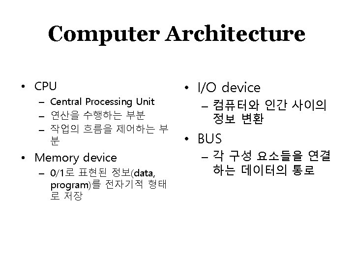
Computer Architecture Read Write CPU Input Device Memory Output Device
Main Memory • ROM (Read Only Memory) – 주로 읽을 수만 있는 장치 – 전원이 끊겨도 내용이 보존됨 – firmware를 저장해 두는 용도로 이용됨 • 예) 부트스트랩 프로그램의 저장 • Special ROMs – PROM: Programmable ROM – EPROM: Erasable PROM – EEPROM: Electrically EPROM