Digital Logic Design n Basics Combinational Circuits Sequential
Digital Logic Design n Basics Combinational Circuits Sequential Circuits Adapted from the slides prepared by S. Dandamudi for the book, Fundamentals of Computer Organization and Design.
Introduction to Digital Logic Basics n Hardware consists of a few simple building blocks Ø n These are called logic gates n AND, OR, NOT, … n NAND, NOR, XOR, … Logic gates are built using transistors n n n NOT gate can be implemented by a single transistor AND gate requires 3 transistors Transistors are the fundamental devices n n n Pentium consists of 3 million transistors Compaq Alpha consists of 9 million transistors Now we can build chips with more than 100 million transistors
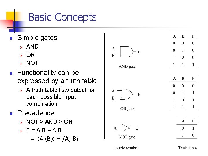
Basic Concepts n Simple gates Ø Ø Ø n Functionality can be expressed by a truth table Ø n AND OR NOT A truth table lists output for each possible input combination Precedence Ø Ø NOT > AND > OR F=AB+AB = (A (B)) + ((A) B)
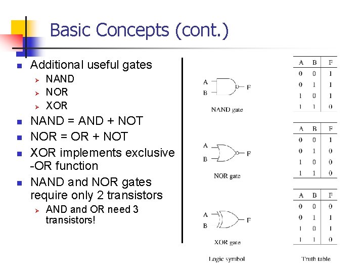
Basic Concepts (cont. ) n Additional useful gates Ø Ø Ø n n NAND NOR XOR NAND = AND + NOT NOR = OR + NOT XOR implements exclusive -OR function NAND and NOR gates require only 2 transistors Ø AND and OR need 3 transistors!
Basic Concepts (cont. ) n Number of functions Ø Ø With N logical variables, we can define N 2 2 functions Some of them are useful n AND, NOR, XOR, … Some are not useful: n Output is always 1 n Output is always 0 “Number of functions” definition is useful in proving completeness property
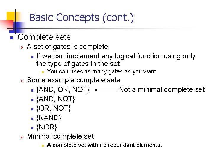
Basic Concepts (cont. ) n Complete sets Ø A set of gates is complete n If we can implement any logical function using only the type of gates in the set n Ø Ø You can uses as many gates as you want Some example complete sets n {AND, OR, NOT} Not a minimal complete set n {AND, NOT} n {OR, NOT} n {NAND} n {NOR} Minimal complete set n A complete set with no redundant elements.
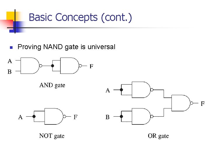
Basic Concepts (cont. ) n Proving NAND gate is universal
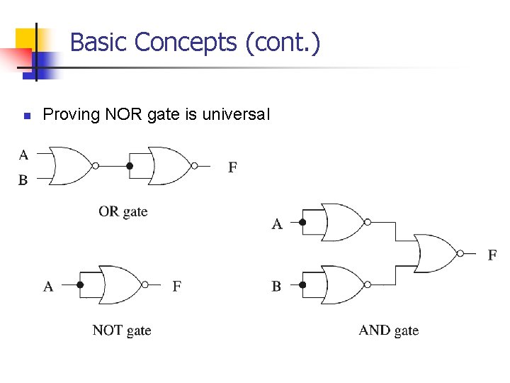
Basic Concepts (cont. ) n Proving NOR gate is universal
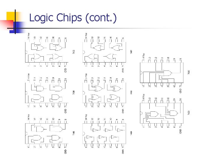
Logic Chips (cont. )
Logic Chips (cont. ) n Integration levels Ø Ø SSI (small scale integration) n Introduced in late 1960 s n 1 -10 gates (previous examples) MSI (medium scale integration) n Introduced in late 1960 s n 10 -100 gates LSI (large scale integration) n Introduced in early 1970 s n 100 -10, 000 gates VLSI (very large scale integration) n Introduced in late 1970 s n More than 10, 000 gates
Logic Functions n Logical functions can be expressed in several ways: Ø Ø Ø n Truth table Logical expressions Graphical form Example: Ø Majority function n Output is one whenever majority of inputs is 1 n We use 3 -input majority function
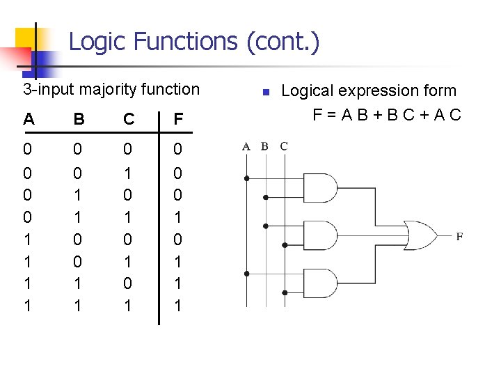
Logic Functions (cont. ) 3 -input majority function A B C F 0 0 1 1 0 1 0 1 0 0 0 1 1 1 n Logical expression form F=AB+BC+AC
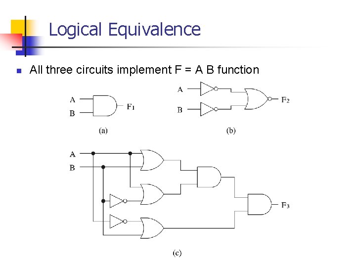
Logical Equivalence n All three circuits implement F = A B function

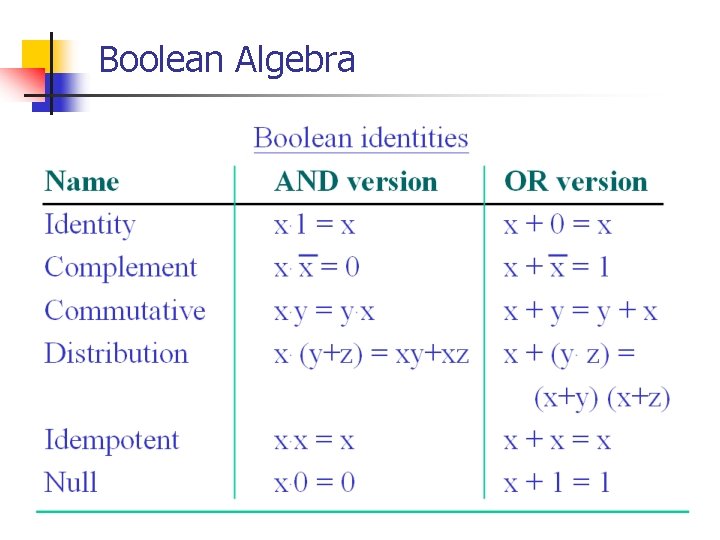
Logical Equivalence (cont. ) n Proving logical equivalence of two circuits Ø Ø Derive the logical expression for the output of each circuit Show that these two expressions are equivalent n Two ways: n n You can use the truth table method n For every combination of inputs, if both expressions yield the same output, they are equivalent n Good for logical expressions with small number of variables You can also use algebraic manipulation n Need Boolean identities
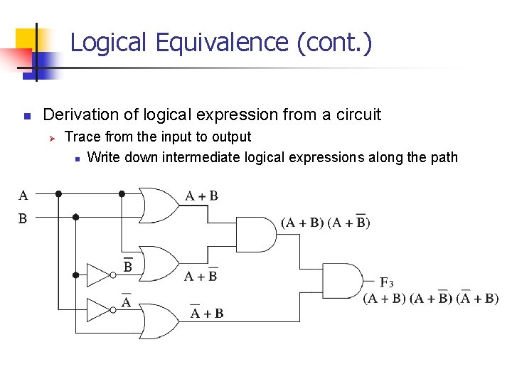
Logical Equivalence (cont. ) n Derivation of logical expression from a circuit Ø Trace from the input to output n Write down intermediate logical expressions along the path
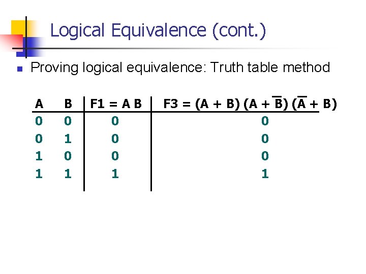
Logical Equivalence (cont. ) n Proving logical equivalence: Truth table method A 0 0 1 1 B 0 1 F 1 = A B 0 0 0 1 F 3 = (A + B) 0 0 0 1
Boolean Algebra
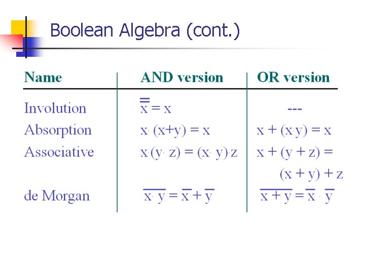
Boolean Algebra (cont. )

Boolean Algebra (cont. ) n Proving logical equivalence: Boolean algebra method Ø To prove that two logical functions F 1 and F 2 are equivalent n Start with one function and apply Boolean laws to derive the other function n Needs intuition as to which laws should be applied and when n Sometimes it may be convenient to reduce both functions to the same expression Example: F 1= A B and F 3 are equivalent n Ø Practice helps
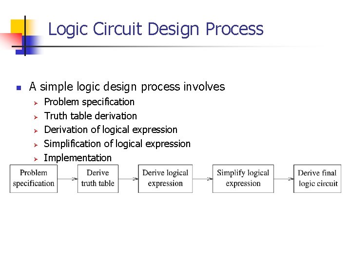
Logic Circuit Design Process n A simple logic design process involves Ø Ø Ø Problem specification Truth table derivation Derivation of logical expression Simplification of logical expression Implementation
Deriving Logical Expressions n Derivation of logical expressions from truth tables Ø Ø n SOP form Ø Ø n sum-of-products (SOP) form product-of-sums (POS) form Write an AND term for each input combination that produces a 1 output n Write the variable if its value is 1; complement otherwise OR the AND terms to get the final expression POS form Ø Dual of the SOP form
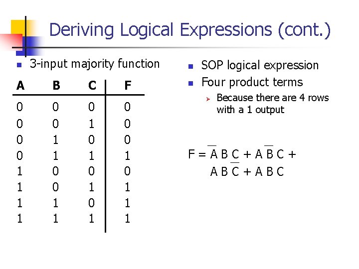
Deriving Logical Expressions (cont. ) n A 0 0 1 1 3 -input majority function B 0 0 1 1 C 0 1 0 1 F 0 0 0 1 1 1 n n SOP logical expression Four product terms Ø Because there are 4 rows with a 1 output F=ABC+ABC
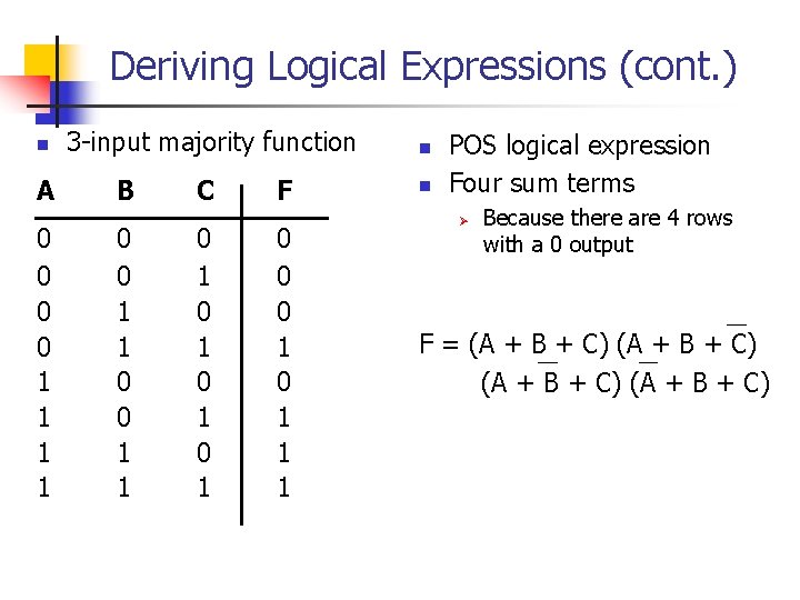
Deriving Logical Expressions (cont. ) n A 0 0 1 1 3 -input majority function B 0 0 1 1 C 0 1 0 1 F 0 0 0 1 1 1 n n POS logical expression Four sum terms Ø Because there are 4 rows with a 0 output F = (A + B + C)
Logical Expression Simplification Ø Algebraic manipulation n Use Boolean laws to simplify the expression n n Difficult to use Don’t know if you have the simplified form

Algebraic Manipulation n Majority function example Added extra ABC+ABC+ABC = ABC+ABC+ABC+ABC n We can now simplify this expression as BC+AC+AB n A difficult method to use for complex expressions
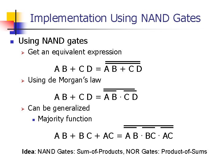
Implementation Using NAND Gates n Using NAND gates Ø Get an equivalent expression AB+CD=AB+CD Ø Using de Morgan’s law AB+CD=AB. CD Ø Can be generalized n Majority function A B + B C + AC = A B. BC. AC Idea: NAND Gates: Sum-of-Products, NOR Gates: Product-of-Sums
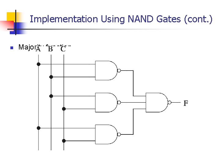
Implementation Using NAND Gates (cont. ) n Majority function
Introduction to Combinational Circuits n Combinational circuits n n Combinational circuits provide a higher level of abstraction Ø Ø n Output depends only on the current inputs Help in reducing design complexity Reduce chip count We look at some useful combinational circuits
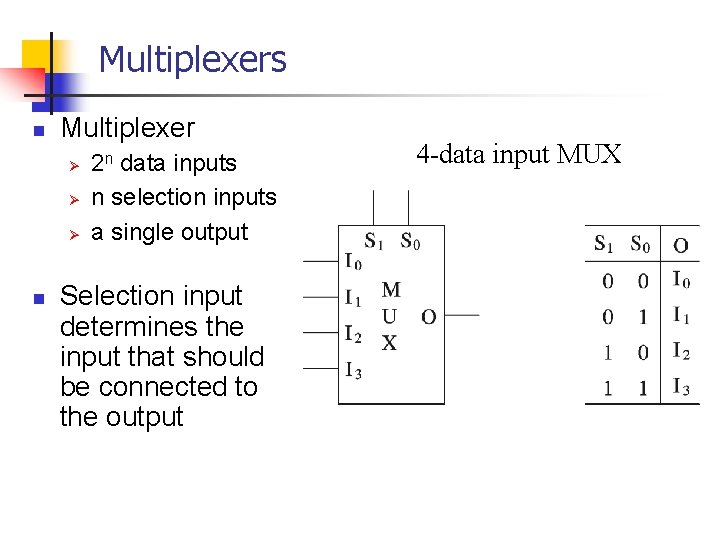
Multiplexers n Multiplexer Ø Ø Ø n 2 n data inputs n selection inputs a single output Selection input determines the input that should be connected to the output 4 -data input MUX
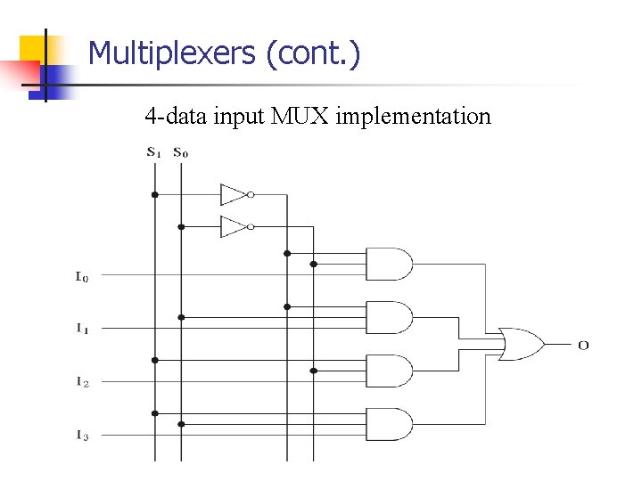
Multiplexers (cont. ) 4 -data input MUX implementation
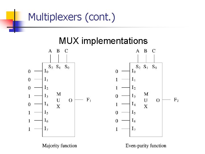
Multiplexers (cont. ) MUX implementations
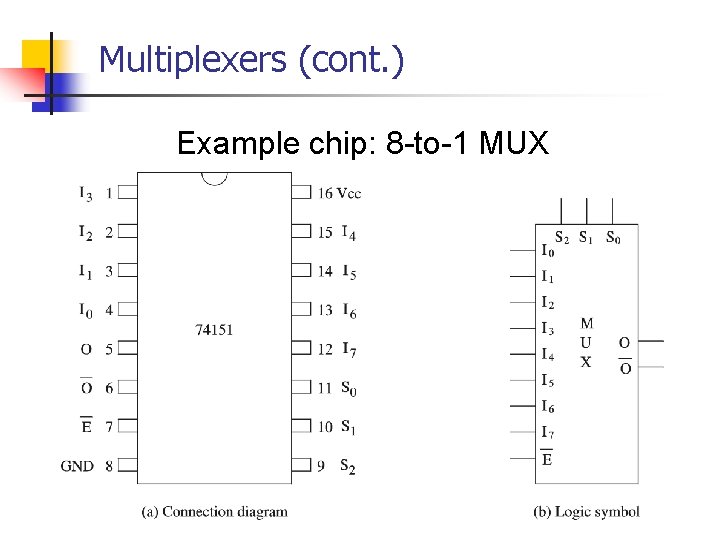
Multiplexers (cont. ) Example chip: 8 -to-1 MUX
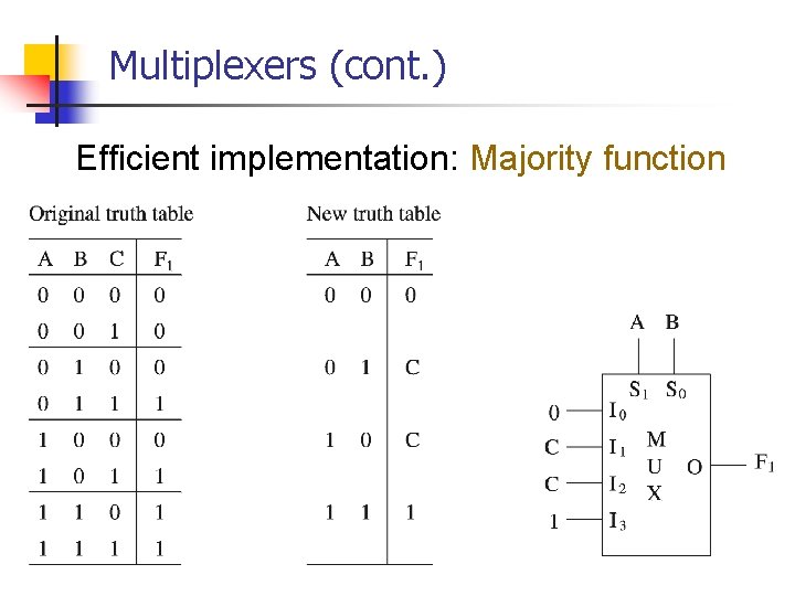
Multiplexers (cont. ) Efficient implementation: Majority function
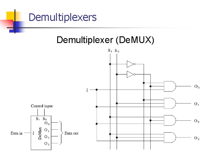
Demultiplexers Demultiplexer (De. MUX)
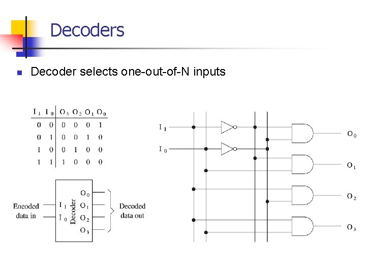
Decoders n Decoder selects one-out-of-N inputs
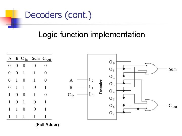
Decoders (cont. ) Logic function implementation (Full Adder)
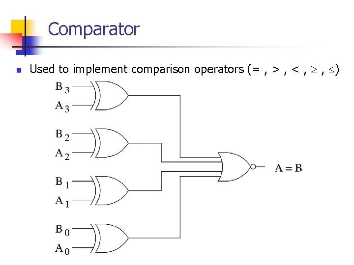
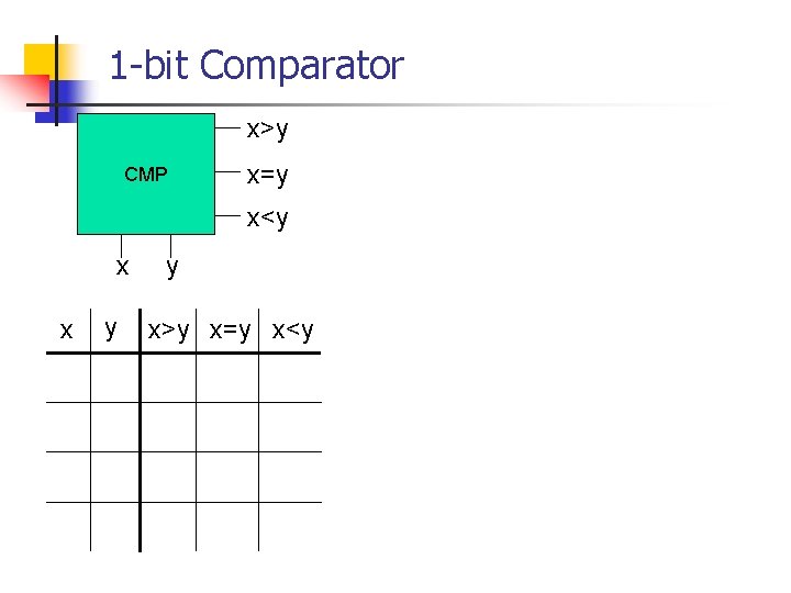
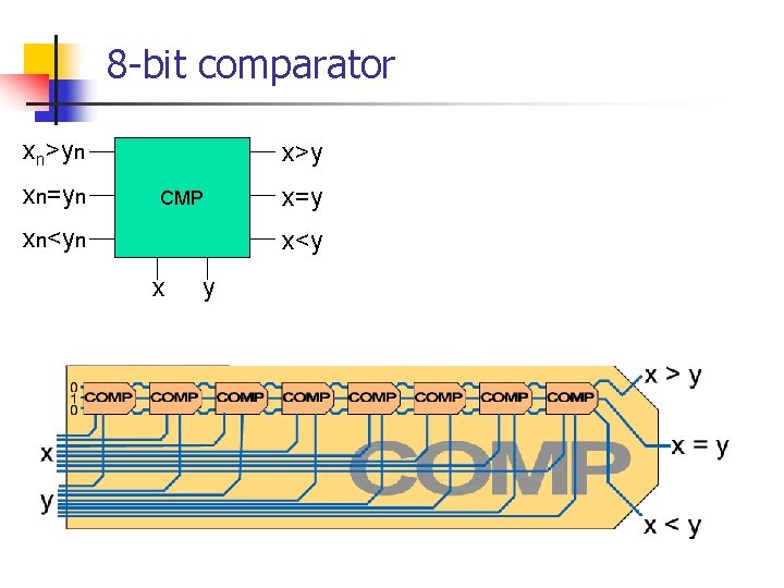
Comparator n Used to implement comparison operators (= , > , < , , )
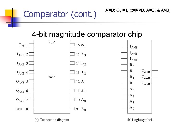
Comparator (cont. ) A=B: Ox = Ix (x=A<B, A=B, & A>B) 4 -bit magnitude comparator chip
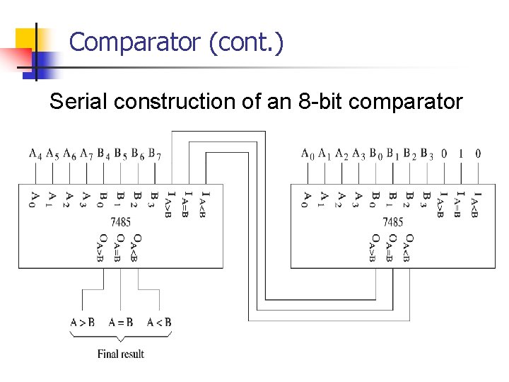
Comparator (cont. ) Serial construction of an 8 -bit comparator
1 -bit Comparator x>y CMP x=y x<y x x y y x>y x=y x<y
8 -bit comparator xn>yn xn=yn x>y CMP xn<yn x=y x<y x y
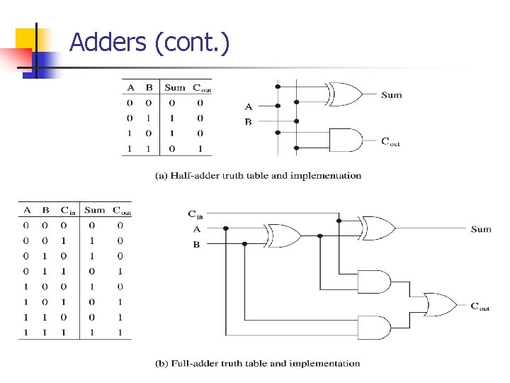
Adders n Half-adder Ø Ø n Adds two bits n Produces a sum and carry Problem: Cannot use it to build larger inputs Full-adder Ø Ø Adds three 1 -bit values n Like half-adder, produces a sum and carry Allows building N-bit adders n Simple technique n n Connect Cout of one adder to Cin of the next These are called ripple-carry adders
Adders (cont. )
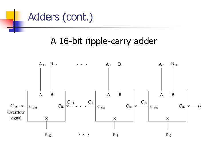
Adders (cont. ) A 16 -bit ripple-carry adder
Adders (cont. ) n Ripple-carry adders can be slow Ø n Delay proportional to number of bits Carry lookahead adders Ø Ø Eliminate the delay of ripple-carry adders Carry-ins are generated independently n C 0 = A 0 B 0 n C 1 = A 0 B 0 A 1 + A 0 B 1 + A 1 B 1 . . . Requires complex circuits Usually, a combination carry lookahead and ripple-carry techniques are used n Ø Ø
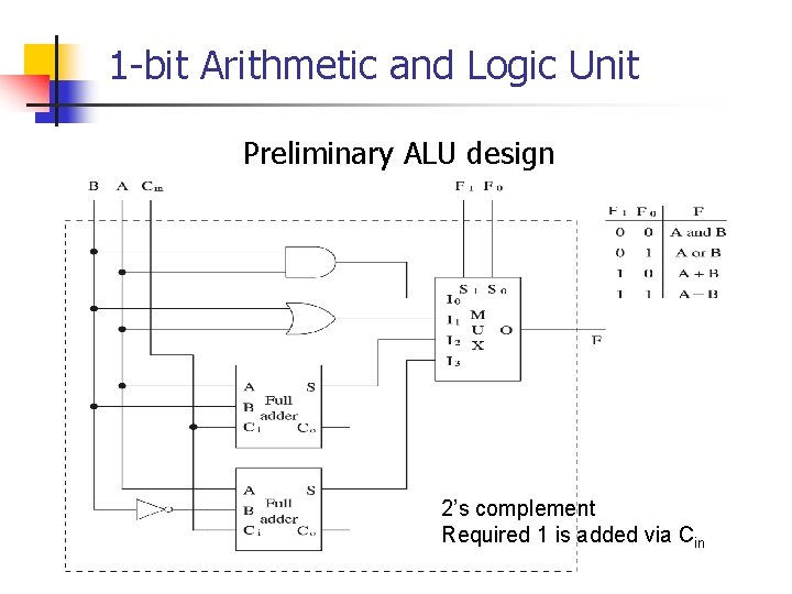
1 -bit Arithmetic and Logic Unit Preliminary ALU design 2’s complement Required 1 is added via Cin
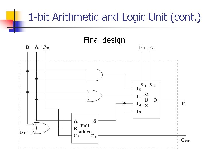
1 -bit Arithmetic and Logic Unit (cont. ) Final design
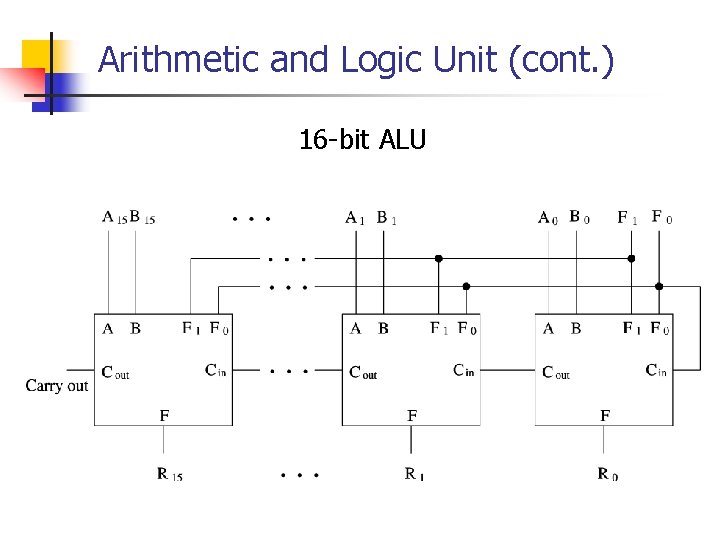
Arithmetic and Logic Unit (cont. ) 16 -bit ALU
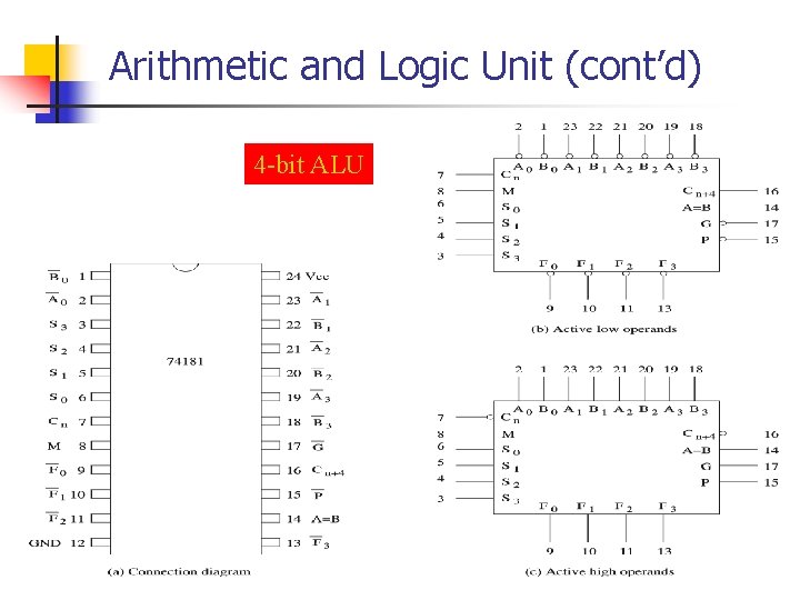
Arithmetic and Logic Unit (cont’d) 4 -bit ALU
- Slides: 49