Tutorial 6 Digital Logic Design ELCT 201 Spring


![Decoders [n-to-2 n] For each possible i/p combination there are : 2 n – Decoders [n-to-2 n] For each possible i/p combination there are : 2 n –](https://slidetodoc.com/presentation_image_h/7fb9c35d65aaea90d2f33bc80a2963f2/image-3.jpg)
![[n-to-2 n] Decoders n: 2 n decoder 3 -to-8 For. Decoder each possible i/p [n-to-2 n] Decoders n: 2 n decoder 3 -to-8 For. Decoder each possible i/p](https://slidetodoc.com/presentation_image_h/7fb9c35d65aaea90d2f33bc80a2963f2/image-4.jpg)
![n] Decoders [NAND [n-to-2 based] n: 2 n decoder 3 -to-8 Decoder no. of n] Decoders [NAND [n-to-2 based] n: 2 n decoder 3 -to-8 Decoder no. of](https://slidetodoc.com/presentation_image_h/7fb9c35d65aaea90d2f33bc80a2963f2/image-5.jpg)
![n] Decoders [NAND [n-to-2 based] n: 2 n decoder 3 -to-8 Decoder NAND based n] Decoders [NAND [n-to-2 based] n: 2 n decoder 3 -to-8 Decoder NAND based](https://slidetodoc.com/presentation_image_h/7fb9c35d65aaea90d2f33bc80a2963f2/image-6.jpg)
![Decoder [with Enable Line]: [1 st Use: To Control the Circuit Operation] Sheet 6 Decoder [with Enable Line]: [1 st Use: To Control the Circuit Operation] Sheet 6](https://slidetodoc.com/presentation_image_h/7fb9c35d65aaea90d2f33bc80a2963f2/image-7.jpg)
![Decoder [with Enable Line]: 2 graphical representations of NOR: Invert-AND OR-invert [1 st Use: Decoder [with Enable Line]: 2 graphical representations of NOR: Invert-AND OR-invert [1 st Use:](https://slidetodoc.com/presentation_image_h/7fb9c35d65aaea90d2f33bc80a2963f2/image-8.jpg)
![Decoder [with Enable Line]: [1 st Use: To Control the Circuit Operation] Sheet 6 Decoder [with Enable Line]: [1 st Use: To Control the Circuit Operation] Sheet 6](https://slidetodoc.com/presentation_image_h/7fb9c35d65aaea90d2f33bc80a2963f2/image-9.jpg)
![Decoder [with Enable Line]: [1 st Use: To Control the Circuit Operation] no. of Decoder [with Enable Line]: [1 st Use: To Control the Circuit Operation] no. of](https://slidetodoc.com/presentation_image_h/7fb9c35d65aaea90d2f33bc80a2963f2/image-10.jpg)
![Decoder with Enable Line: [2 nd Use: implementing bigger decoders] wxyz 0000 z y Decoder with Enable Line: [2 nd Use: implementing bigger decoders] wxyz 0000 z y](https://slidetodoc.com/presentation_image_h/7fb9c35d65aaea90d2f33bc80a2963f2/image-11.jpg)
![Decoder with Enable Line: [2 nd Use: implementing bigger decoders] wxyz 0000 0 0 Decoder with Enable Line: [2 nd Use: implementing bigger decoders] wxyz 0000 0 0](https://slidetodoc.com/presentation_image_h/7fb9c35d65aaea90d2f33bc80a2963f2/image-12.jpg)
![Decoder with Enable Line: [2 nd Use: implementing bigger decoders] wxyz 1111 1 1 Decoder with Enable Line: [2 nd Use: implementing bigger decoders] wxyz 1111 1 1](https://slidetodoc.com/presentation_image_h/7fb9c35d65aaea90d2f33bc80a2963f2/image-13.jpg)
![Encoders ≠ Decoders [2 n-to-n] Example: 8 -to-3 Encoder n: 2 n decoder 2 Encoders ≠ Decoders [2 n-to-n] Example: 8 -to-3 Encoder n: 2 n decoder 2](https://slidetodoc.com/presentation_image_h/7fb9c35d65aaea90d2f33bc80a2963f2/image-16.jpg)

![Encoders ≠ Decoders [2 n-to-n] Example: 8 -to-3 Encoder D 7 D 6 D Encoders ≠ Decoders [2 n-to-n] Example: 8 -to-3 Encoder D 7 D 6 D](https://slidetodoc.com/presentation_image_h/7fb9c35d65aaea90d2f33bc80a2963f2/image-18.jpg)
![Multiplexer [ 2 n to 1 with n selection lines] 2 n inputs Example: Multiplexer [ 2 n to 1 with n selection lines] 2 n inputs Example:](https://slidetodoc.com/presentation_image_h/7fb9c35d65aaea90d2f33bc80a2963f2/image-22.jpg)
![Multiplexer [ 2 n to 1 with n selection lines] 2 n inputs Example: Multiplexer [ 2 n to 1 with n selection lines] 2 n inputs Example:](https://slidetodoc.com/presentation_image_h/7fb9c35d65aaea90d2f33bc80a2963f2/image-23.jpg)

- Slides: 35

Tutorial 6 Digital Logic Design (ELCT 201) – Spring 2020 Eng. Minar El-Aasser

Agenda • Decoders • Encoders • Multiplexers • Tri-State Buffers
![Decoders nto2 n For each possible ip combination there are 2 n Decoders [n-to-2 n] For each possible i/p combination there are : 2 n –](https://slidetodoc.com/presentation_image_h/7fb9c35d65aaea90d2f33bc80a2963f2/image-3.jpg)
Decoders [n-to-2 n] For each possible i/p combination there are : 2 n – 1 o/p(s) that are equal to 0 and ONLY ONE o/p that is equal to 1 The o/p whose value=1 represents the min-term equivalent to the binary no. presently available in the i/p lines. 3 -to-8 Decoder no. of i/p(s) = 3 no. of o/p(s) = 23 =8 x y z Do D 1 D 2 D 3 D 4 D 5 D 6 D 7 0 0 0 1 0 0 0 0 1 0 0 0 0 1 0 0 0 1 0 0 0 1 1 0 0 0 0 1 1 1 0 0 0 0 1
![nto2 n Decoders n 2 n decoder 3 to8 For Decoder each possible ip [n-to-2 n] Decoders n: 2 n decoder 3 -to-8 For. Decoder each possible i/p](https://slidetodoc.com/presentation_image_h/7fb9c35d65aaea90d2f33bc80a2963f2/image-4.jpg)
[n-to-2 n] Decoders n: 2 n decoder 3 -to-8 For. Decoder each possible i/p combination there are : n o/p(s) that are equalxto 0 yand z 3 =8 no. of i/p(s) = 3 2 – 1 no. of o/p(s) = 2 ONLY ONE o/p that is equal to 1 x y The z o/p Do whose D 1 D 2 value=1 D 3 D 4 represents D 5 D 6 D 7 the min-term equivalent 0 0 to 0 the 1 binary 0 0 no. 0 presently 0 0 available 0 0 in the i/p lines. 0 0 0 1 1 0 1 0 0 3 -to-8 Decoder 1 0 0 0 no. of 1 1 i/p(s) 0 0= 3 0 1 no. 0 of o/p(s) 0 0 0 0 1 1 0 0 x 0 0 0 y 0 0 1 D 0 =0 x’y’z’ 1 D 1 =1 x’y’z 0 D 2 =1 x’yz’ 0 D 3 =1 xy’z’ 1 1 1 z 0 1 0 0 Do D 1 1 0 0 0 1 0 0 D 1 23 =0 =8 0 D 2 D 3 D 4 D 5 D 6 D 7 0 0 0 0 1 0 0 0 1 1 0 0 0 0 0 1 0 0 0 D 04 = xy’z’ 0 0 D 05 = xy’z 0 0 D 06 = xyz’ 0 0 D 07 = xyz 0 0 0 1 1 0 0 D 2 D 3 D 4 D 5 D 6 D 7
![n Decoders NAND nto2 based n 2 n decoder 3 to8 Decoder no of n] Decoders [NAND [n-to-2 based] n: 2 n decoder 3 -to-8 Decoder no. of](https://slidetodoc.com/presentation_image_h/7fb9c35d65aaea90d2f33bc80a2963f2/image-5.jpg)
n] Decoders [NAND [n-to-2 based] n: 2 n decoder 3 -to-8 Decoder no. of i/p(s) = 3 NAND based N. B. : y z Do D 1 D 2 D 3 Decoders 0 constructed 0 0 1 0 with 0 0 0 NAND 0 1 gates 0 1 -> give 0 0 0 decoders 1 0 0 output 0 1 0 (Min-terms) in their 0 1 1 0 0 0 1 complement form 1 0 0 0 “Active Low o/p” 1 0 0 0 0 • Its is used because it 1 0 0 0 is 1 more economical x • 1 1 1 D 0 = x’y’z’ D 1 = x’y’z D 2 = x’yz’ D 3 = xy’z’ 0 x no. of o/p(s) = 23 =8 0 0 0 D 4 = xy’z’ D 5 = xy’z D 6 = xyz’ D 7 = xyz y z D 4 D 5 D 6 D 7 0 0 0 0 D’ x 0 y z Do D 1 D 2 D 3 0 0 0 0 1 0 1 1 0 0 0 0 D ’ 1 0 0 1 0 1 0 0 1 1 0 1 0 1 1 0 0 0 1 D ’ 0 0 0 1 0 1 0 0 0 1 1 0 1 0 1 1 D 4’ 1 0 0 1 1 1 0 1 D 1’ 0 2 3 D 5’ 1 D 0 D 4 D 5 D 6 D 7 D 101 0 1 0 1 D 102 0 1 0 1 D 013 0 1 0 1 0 1 D 104 1 0 0 1 0 1 1 0 D 5 D 6’ D 6 D 7’ D 7
![n Decoders NAND nto2 based n 2 n decoder 3 to8 Decoder NAND based n] Decoders [NAND [n-to-2 based] n: 2 n decoder 3 -to-8 Decoder NAND based](https://slidetodoc.com/presentation_image_h/7fb9c35d65aaea90d2f33bc80a2963f2/image-6.jpg)
n] Decoders [NAND [n-to-2 based] n: 2 n decoder 3 -to-8 Decoder NAND based x y z N. B. : • Decoders constructed with NAND gates -> give decoders output (Min-terms) in their complement form “Active Low o/p” • Its is used because it is more economical DD 0’ x 0 y z Do D 1 D 2 D 3 D 4 D 5 D 6 D 7 0 0 DD 11’ 0 1 0 1 0 1 1 0 0 1 0 1 0 1 0 DD’ 1 0 0 1 0 1 1 1 0 1 0 1 1 0 0 1 0 1 1 DD 3’ 0 0 0 1 0 1 1 1 0 1 0 1 0 1 1 0 0 1 1 0 1 0 1 1 0 0 0 22 3 0 1 DD 44’ 1 1 DD 55’ DD 66’ DD 77’ 1
![Decoder with Enable Line 1 st Use To Control the Circuit Operation Sheet 6 Decoder [with Enable Line]: [1 st Use: To Control the Circuit Operation] Sheet 6](https://slidetodoc.com/presentation_image_h/7fb9c35d65aaea90d2f33bc80a2963f2/image-7.jpg)
Decoder [with Enable Line]: [1 st Use: To Control the Circuit Operation] Sheet 6 – Problem I Design 2 -4 line decoder using NOR gates only (include an enable input) no. of i/p(s) = 3 no. of o/p(s) = 4 E x y Do D 1 D 2 D 3 0 0 0 0 0 1 0 0 0 1 1 0 0 0 1 1 0 1 0 0 1 0 1 1 1 0 0 0 1 E x y Do D 1 D 2 D 3 0 x x 0 0 1 0 1 0 0 1 1 0 0 0 1
![Decoder with Enable Line 2 graphical representations of NOR InvertAND ORinvert 1 st Use Decoder [with Enable Line]: 2 graphical representations of NOR: Invert-AND OR-invert [1 st Use:](https://slidetodoc.com/presentation_image_h/7fb9c35d65aaea90d2f33bc80a2963f2/image-8.jpg)
Decoder [with Enable Line]: 2 graphical representations of NOR: Invert-AND OR-invert [1 st Use: To Control the Circuit Operation] Sheet 6 – Problem I Design 2 -4 line decoder using NOR gates only (include an enable input) no. of i/p(s) = 3 no. of o/p(s) = 4 E x y Do D 1 D 2 D 3 0 0 0 0 0 1 0 0 0 1 1 0 0 0 1 0 1 0 0 1 1 0 0 0 2 = Exy’ 1 1 D 0= 1 Ex’y’ 1 D 1 = Ex’y 0 D D 3 = Exy E x’ x x y Do D 1 D 2 D 3 x x 0 0 0 1 0 1 0 0 1 1 0 0 0 1 0 1 yy’ EE’ D 0 D 1 D 2 D 3
![Decoder with Enable Line 1 st Use To Control the Circuit Operation Sheet 6 Decoder [with Enable Line]: [1 st Use: To Control the Circuit Operation] Sheet 6](https://slidetodoc.com/presentation_image_h/7fb9c35d65aaea90d2f33bc80a2963f2/image-9.jpg)
Decoder [with Enable Line]: [1 st Use: To Control the Circuit Operation] Sheet 6 – Problem I Design 2 -4 line decoder using NOR gates only (include an enable input) no. of i/p(s) = 3 no. of o/p(s) = 4 x’ x E x y Do D 1 D 2 D 3 0 1 x x 0 0 1 0 0 1 0 1 0 0 0 1 0 1 1 0 0 0 1 yy’ D 0 D 1 D 2 EE’ D 3
![Decoder with Enable Line 1 st Use To Control the Circuit Operation no of Decoder [with Enable Line]: [1 st Use: To Control the Circuit Operation] no. of](https://slidetodoc.com/presentation_image_h/7fb9c35d65aaea90d2f33bc80a2963f2/image-10.jpg)
Decoder [with Enable Line]: [1 st Use: To Control the Circuit Operation] no. of i/p(s) = n+1 no. of o/p(s) = 2 n n: 2 n decoder Enable
![Decoder with Enable Line 2 nd Use implementing bigger decoders wxyz 0000 z y Decoder with Enable Line: [2 nd Use: implementing bigger decoders] wxyz 0000 z y](https://slidetodoc.com/presentation_image_h/7fb9c35d65aaea90d2f33bc80a2963f2/image-11.jpg)
Decoder with Enable Line: [2 nd Use: implementing bigger decoders] wxyz 0000 z y x 1111 w 4 to 16 decoder D 0 D 1 D 2 D 3 D 4 D 5 D 6 D 7 01 00 00 D 8 D 9 D 10 D 11 D 12 D 13 D 14 D 15 00 00 10
![Decoder with Enable Line 2 nd Use implementing bigger decoders wxyz 0000 0 0 Decoder with Enable Line: [2 nd Use: implementing bigger decoders] wxyz 0000 0 0](https://slidetodoc.com/presentation_image_h/7fb9c35d65aaea90d2f33bc80a2963f2/image-12.jpg)
Decoder with Enable Line: [2 nd Use: implementing bigger decoders] wxyz 0000 0 0 z y x w 1 E 4 to 16 decoder 0 E D 0 D 1 D 2 D 3 D 4 D 5 D 6 D 7 1 0 0 0 0 D 1 D 2 D 3 D 4 D 5 D 6 D 7 D 8 D 9 D 10 D 11 D 12 D 13 D 14 D 15 0 0 0 0
![Decoder with Enable Line 2 nd Use implementing bigger decoders wxyz 1111 1 1 Decoder with Enable Line: [2 nd Use: implementing bigger decoders] wxyz 1111 1 1](https://slidetodoc.com/presentation_image_h/7fb9c35d65aaea90d2f33bc80a2963f2/image-13.jpg)
Decoder with Enable Line: [2 nd Use: implementing bigger decoders] wxyz 1111 1 1 z y x w 0 E 4 to 16 decoder 1 E D 0 D 1 D 2 D 3 D 4 D 5 D 6 D 7 0 0 0 0 D 0 D 1 D 2 D 3 D 4 D 5 D 6 D 7 D 8 D 9 D 10 D 11 D 12 D 13 D 14 D 15 0 0 0 0 1

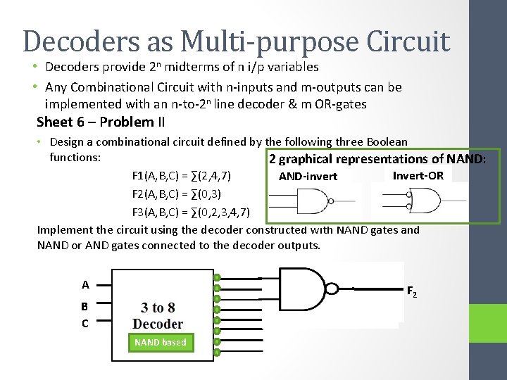
Decoders as Multi-purpose Circuit • Decoders provide 2 n midterms of n i/p variables • Any Combinational Circuit with n-inputs and m-outputs can be implemented with an n-to-2 n line decoder & m OR-gates Sheet 6 – Problem II • Design a combinational circuit defined by the following three Boolean functions: 2 graphical representations of NAND: Invert-OR F 1(A, B, C) = ∑(2, 4, 7) AND-invert F 2(A, B, C) = ∑(0, 3) F 3(A, B, C) = ∑(0, 2, 3, 4, 7) Implement the circuit using the decoder constructed with NAND gates and NAND or AND gates connected to the decoder outputs. A F 2 B C NAND based

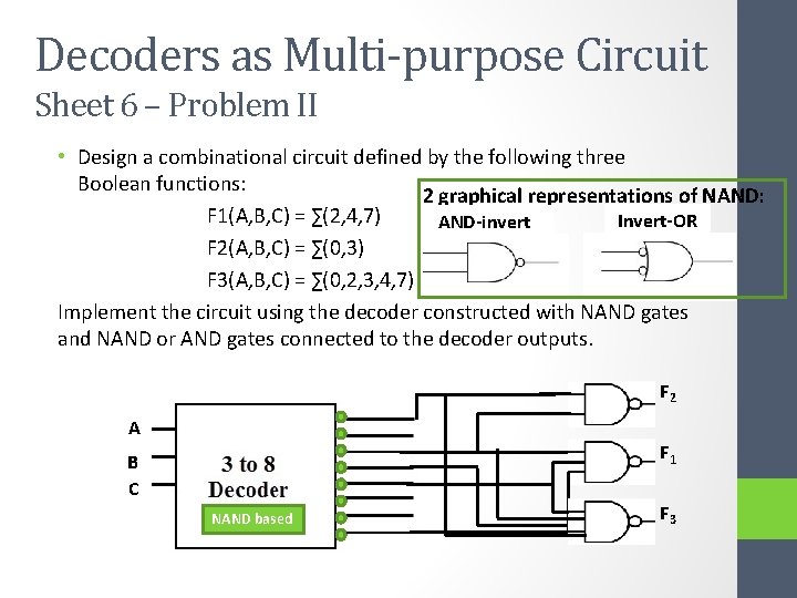
Decoders as Multi-purpose Circuit Sheet 6 – Problem II • Design a combinational circuit defined by the following three Boolean functions: 2 graphical representations of NAND: F 1(A, B, C) = ∑(2, 4, 7) Invert-OR AND-invert F 2(A, B, C) = ∑(0, 3) F 3(A, B, C) = ∑(0, 2, 3, 4, 7) Implement the circuit using the decoder constructed with NAND gates and NAND or AND gates connected to the decoder outputs. F 2 A F 1 B C NAND based F 3
![Encoders Decoders 2 nton Example 8 to3 Encoder n 2 n decoder 2 Encoders ≠ Decoders [2 n-to-n] Example: 8 -to-3 Encoder n: 2 n decoder 2](https://slidetodoc.com/presentation_image_h/7fb9c35d65aaea90d2f33bc80a2963f2/image-16.jpg)
Encoders ≠ Decoders [2 n-to-n] Example: 8 -to-3 Encoder n: 2 n decoder 2 n : n Encoder

![Encoders Decoders 2 nton Example 8 to3 Encoder D 7 D 6 D Encoders ≠ Decoders [2 n-to-n] Example: 8 -to-3 Encoder D 7 D 6 D](https://slidetodoc.com/presentation_image_h/7fb9c35d65aaea90d2f33bc80a2963f2/image-18.jpg)
Encoders ≠ Decoders [2 n-to-n] Example: 8 -to-3 Encoder D 7 D 6 D 5 D 4 D 3 D 2 D 1 D 0 x y z 0 0 0 0 0 0 1 0 0 0 0 0 1 1 0 0 0 0 0 1 1 1 0 0 ? ? 1 0 0 0 0 0 1 0 1 0 0 0 1 1 0 0 0 0 1 1 1 0 0 Encoder Limitations: 1. An o/p with all 0’s will be generated when all i/ps are zero’s; which is the same o/p as when D 0 = 1 Valid Bit 2. Only 1 i/p can be active at any given time. If 2 i/ps are active simultaneously, the o/p produces an undefined combination Priority Fn.

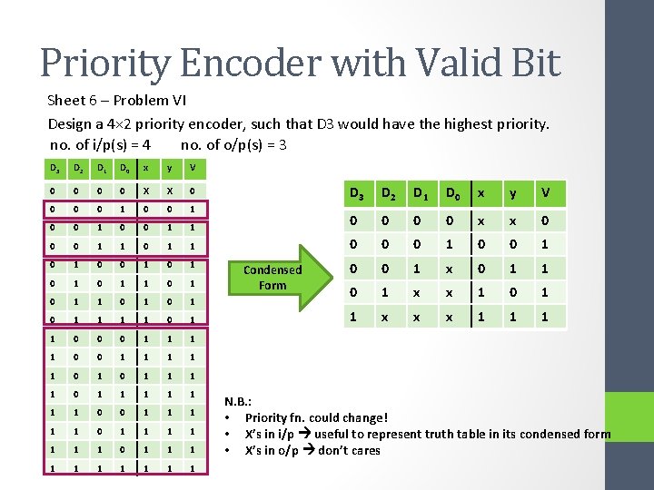
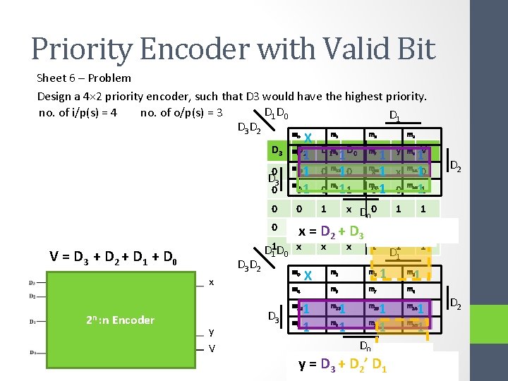
Priority Encoder with Valid Bit Sheet 6 – Problem VI Design a 4× 2 priority encoder, such that D 3 would have the highest priority. no. of i/p(s) = 4 no. of o/p(s) = 3 D 2 D 1 D 0 x y V 0 0 X X 0 0 1 0 0 1 1 0 0 0 1 0 D 3 D 2 D 1 D 0 x y V 1 0 0 x x 0 1 1 0 0 0 1 1 1 0 0 1 x 0 1 1 1 0 1 0 1 x x 1 0 1 1 x x x 1 1 0 0 0 1 1 1 1 1 0 1 1 1 1 0 0 1 1 1 1 0 1 1 1 1 1 Condensed Form N. B. : • Priority fn. could change! • X’s in i/p useful to represent truth table in its condensed form • X’s in o/p don’t cares

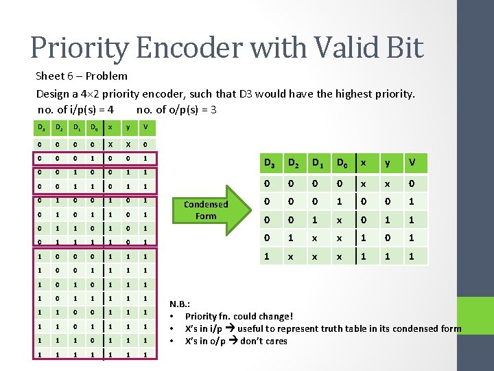
Priority Encoder with Valid Bit Sheet 6 – Problem Design a 4× 2 priority encoder, such that D 3 would have the highest priority. no. of i/p(s) = 4 no. of o/p(s) = 3 D 2 D 1 D 0 x y V 0 0 X X 0 0 1 0 0 1 1 0 1 0 1 1 0 1 0 1 0 1 0 0 0 1 1 0 1 D 3 D 2 D 1 D 0 x y V 0 0 x x 0 0 1 x 0 1 1 1 0 1 x x 1 0 1 1 x x x 1 1 1 0 1 1 1 1 1 0 0 1 1 1 1 0 1 1 1 1 1 Condensed Form N. B. : • Priority fn. could change! • X’s in i/p useful to represent truth table in its condensed form • X’s in o/p don’t cares

Priority Encoder with Valid Bit Sheet 6 – Problem Design a 4× 2 priority encoder, such that D 3 would have the highest priority. D 1 D 0 no. of i/p(s) = 4 no. of o/p(s) = 3 D 1 D 3 D 2 m m 0 X m. D 2 1 m 01 0 0 0 1 x o D 3 0 D 3 V = D 3 + D 2 + D 1 + D 0 D 3 D 2 2 n : n Encoder y V D 1 m 5 D 0 12 13 8 mo m 12 m 8 2 x 1 0 m 10 m 0 11 1 m x 1 m 01 m 7 15 9 11 1 = X m 4 D 3 3 4 D 11 D 0 x x 1 1 1 x D 0 0 x + x. D 1 D x 2 x 3 1 m 3 m 5 m 7 1 m 15 m 13 9 m 11 D 0 y m 6 x m 14 0 m 10 1 1 1 D 1 1 1 V 10 11 D 2 1 m 2 m 6 1 1 yx == D D 3 + D 2 ’ D 1 3 m 14 m 10 1 1 D 2
![Multiplexer 2 n to 1 with n selection lines 2 n inputs Example Multiplexer [ 2 n to 1 with n selection lines] 2 n inputs Example:](https://slidetodoc.com/presentation_image_h/7fb9c35d65aaea90d2f33bc80a2963f2/image-22.jpg)
Multiplexer [ 2 n to 1 with n selection lines] 2 n inputs Example: 2 -to-1 MUX • • 21 inputs Io, I 1 1 inputs Y 1 selection lines S Function Table S Y 0 Io 1 I 1 1 output n selection lines • Truth Table
![Multiplexer 2 n to 1 with n selection lines 2 n inputs Example Multiplexer [ 2 n to 1 with n selection lines] 2 n inputs Example:](https://slidetodoc.com/presentation_image_h/7fb9c35d65aaea90d2f33bc80a2963f2/image-23.jpg)
Multiplexer [ 2 n to 1 with n selection lines] 2 n inputs Example: 2 -to-1 MUX • • 21 inputs Io, I 1 1 inputs Y 1 selection lines S Function Table S Y 0 Io 1 I 1 1 output n selection lines • Truth Table S I 1 o I 0 o Y 0 0 0 1 1 0 0 0 1 1 0 0 1 1 1 S I 1 I 0 0 S 1 I 1 00 01 mo m 1 m 4 m 5 11 m 3 1 m 7 1 1 10 m 2 m 6 I 0 Y = S’I 0 + SI 1 I 0 2: 1 MUX I 1 S y 1

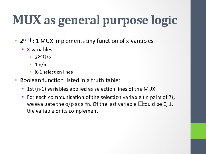
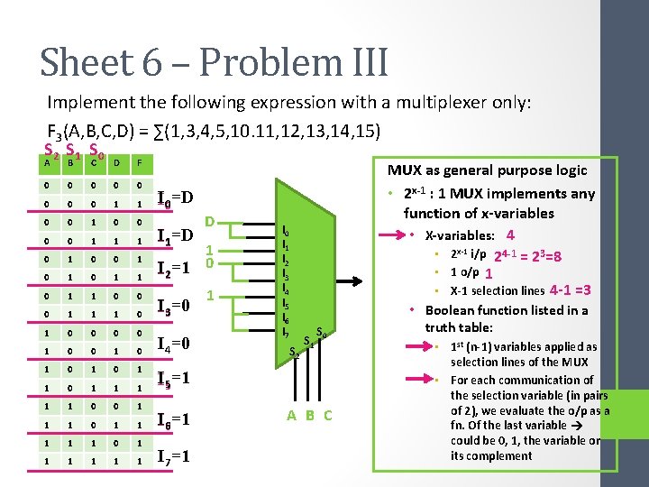
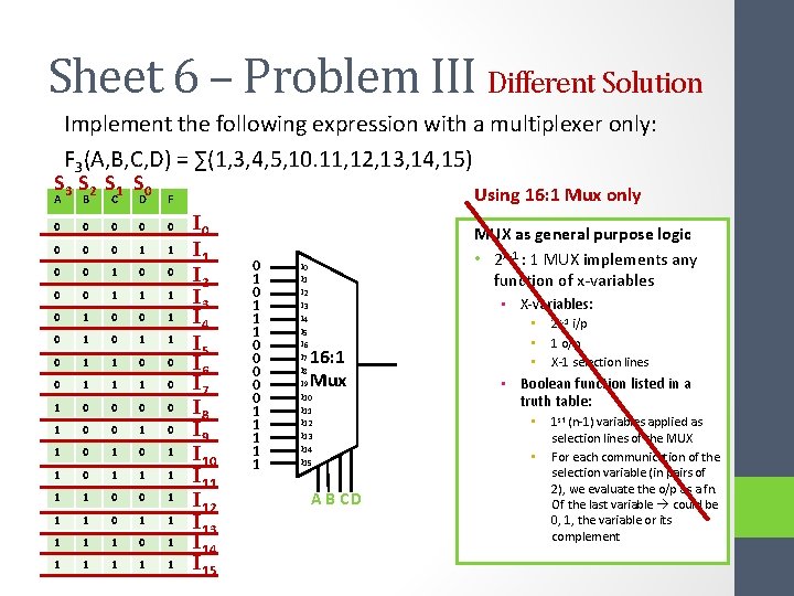
MUX as general purpose logic • 2(x-1) : 1 MUX implements any function of x-variables • X-variables: • 2(x-1) i/p • 1 o/p • X-1 selection lines • Boolean function listed in a truth table: • 1 st (n-1) variables applied as selection lines of the MUX • For each communication of the selection variable (in pairs of 2), we evaluate the o/p as a fn. Of the last variable �could be 0, 1, the variable or its complement

Sheet 6 – Problem III Implement the following expression with a multiplexer only: F 3(A, B, C, D) = ∑(1, 3, 4, 5, 10. 11, 12, 13, 14, 15) S 2 S 1 S 0 A B C D F 0 0 0 0 1 1 1 0 0 1 0 1 1 0 0 0 1 1 1 0 0 0 0 1 0 1 0 1 1 1 1 1 0 1 1 1 I 0=D I 1=D D 1 I 2=1 0 I 3=0 I 4=0 1 I 0 I 1 I 2 I 3 I 4 I 5 I 6 I 7 S 2 MUX as general purpose logic • 2 x-1 : 1 MUX implements any function of x-variables • X-variables: 4 • 2 x-1 i/p 24 -1 = 23=8 • 1 o/p 1 • X-1 selection lines 4 -1 =3 S 1 S 0 I 5=1 I 6=1 I 7=1 A B C • Boolean function listed in a truth table: • 1 st (n-1) variables applied as selection lines of the MUX • For each communication of the selection variable (in pairs of 2), we evaluate the o/p as a fn. Of the last variable could be 0, 1, the variable or its complement

Sheet 6 – Problem III Different Solution Implement the following expression with a multiplexer only: F 3(A, B, C, D) = ∑(1, 3, 4, 5, 10. 11, 12, 13, 14, 15) S 3 S 2 S 1 S 0 A B C D F 0 0 0 0 1 1 1 0 0 1 0 1 1 0 0 0 1 1 1 0 0 0 0 1 0 1 0 1 1 1 1 1 0 1 1 1 Using 16: 1 Mux only I 0 I 1 I 2 I 3 I 4 I 5 I 6 I 7 I 8 I 9 I 10 I 11 I 12 I 13 I 14 I 15 0 1 1 1 0 0 0 1 1 1 I 0 I 1 I 2 I 3 I 4 I 5 I 6 I 7 I 8 I 9 I 10 I 11 I 12 I 13 I 14 I 15 16: 1 Mux A B CD MUX as general purpose logic • 2 x-1 : 1 MUX implements any function of x-variables • X-variables: • • • 2 x-1 i/p 1 o/p X-1 selection lines • Boolean function listed in a truth table: • • 1 st (n-1) variables applied as selection lines of the MUX For each communication of the selection variable (in pairs of 2), we evaluate the o/p as a fn. Of the last variable could be 0, 1, the variable or its complement

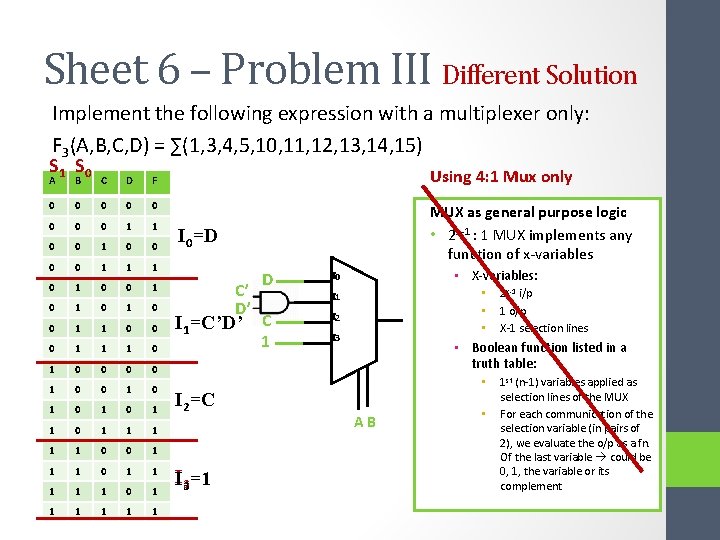
Sheet 6 – Problem III Different Solution Implement the following expression with a multiplexer only: F 3(A, B, C, D) = ∑(1, 3, 4, 5, 10, 11, 12, 13, 14, 15) S 1 S 0 A B C D F 0 0 0 0 1 1 1 0 0 1 0 1 0 0 1 1 0 0 0 1 1 1 0 0 0 0 1 0 1 0 1 1 1 1 1 0 1 1 1 Using 4: 1 Mux only MUX as general purpose logic • 2 x-1 : 1 MUX implements any function of x-variables I 0=D D I 0 I 1=C’D’ C I 2 C’ D’ 1 I 2=C I 3=1 • X-variables: • • • I 1 I 3 2 x-1 i/p 1 o/p X-1 selection lines • Boolean function listed in a truth table: • AB • 1 st (n-1) variables applied as selection lines of the MUX For each communication of the selection variable (in pairs of 2), we evaluate the o/p as a fn. Of the last variable could be 0, 1, the variable or its complement

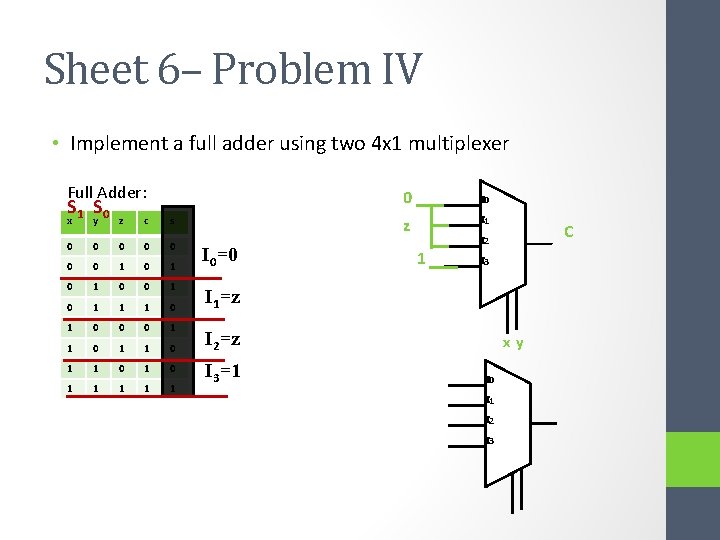
Sheet 6– Problem IV • Implement a full adder using two 4 x 1 multiplexer Full Adder: S 1 S 0 x y z c s 0 0 0 0 1 0 1 0 1 1 1 0 0 0 1 1 0 1 1 1 I 0=0 0 I 0 z I 1 1 C I 2 I 3 I 1=z I 2=z I 3=1 xy I 0 I 1 I 2 I 3

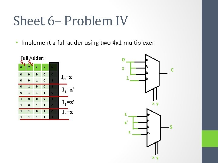
Sheet 6– Problem IV • Implement a full adder using two 4 x 1 multiplexer Full Adder: S 1 S 0 x y z c s 0 0 0 0 1 0 1 0 1 1 1 0 0 0 1 1 0 1 1 1 I 0=z 0 I 0 z I 1 1 C I 2 I 3 I 1=z’ I 2=z’ I 3=z xy z I 0 z' I 1 z S I 2 I 3 xy

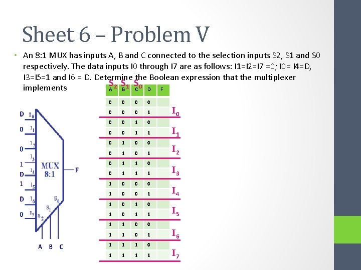
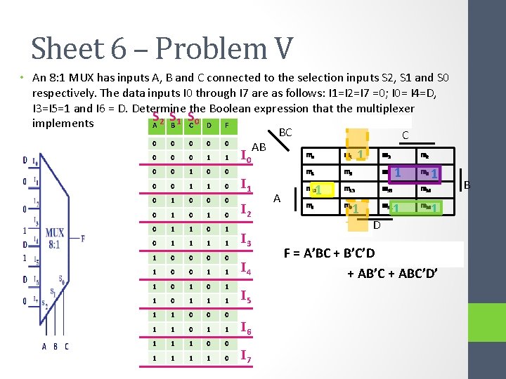
Sheet 6 – Problem V • An 8: 1 MUX has inputs A, B and C connected to the selection inputs S 2, S 1 and S 0 respectively. The data inputs I 0 through I 7 are as follows: I 1=I 2=I 7 =0; I 0= I 4=D, I 3=I 5=1 and I 6 = D. Determine the Boolean expression that the multiplexer SA 2 SB 1 SC 0 D F implements 0 0 0 0 1 1 0 0 0 1 0 1 1 0 0 0 1 1 0 1 0 1 1 0 0 1 1 1 1 0 1 1 I 0 I 1 I 2 I 3 I 4 I 5 I 6 I 7

Sheet 6 – Problem V • An 8: 1 MUX has inputs A, B and C connected to the selection inputs S 2, S 1 and S 0 respectively. The data inputs I 0 through I 7 are as follows: I 1=I 2=I 7 =0; I 0= I 4=D, I 3=I 5=1 and I 6 = D. Determine the Boolean expression that the multiplexer SA 2 SB 1 SC 0 D F implements BC C 0 0 0 AB m m 0 0 0 1 1 0 0 0 0 1 1 0 1 1 1 0 0 1 1 1 0 1 1 1 0 0 0 1 1 1 1 1 0 0 1 1 0 I 1 I 2 I 3 I 4 I 5 I 6 I 7 A 1 o 1 m 4 m 5 m 7 m 12 m 13 m 15 m 8 m 9 1 1 3 m 11 D 2 1 m 6 1 m 14 1 m 10 1 F = A’BC + B’C’D + AB’C + ABC’D’ B

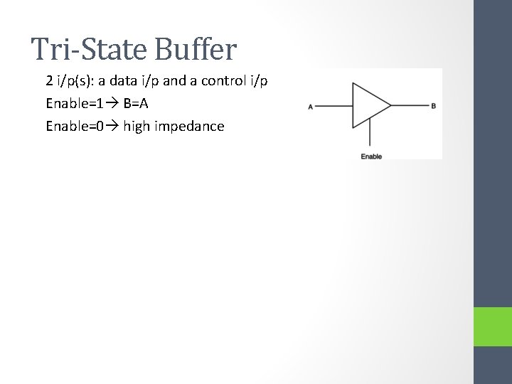
Tri-State Buffer 2 i/p(s): a data i/p and a control i/p Enable=1 B=A Enable=0 high impedance

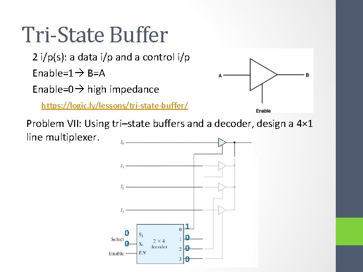
Tri-State Buffer 2 i/p(s): a data i/p and a control i/p Enable=1 B=A Enable=0 high impedance https: //logic. ly/lessons/tri-state-buffer/ Problem VII: Using tri–state buffers and a decoder, design a 4× 1 line multiplexer. 0 0 1 0 0 0

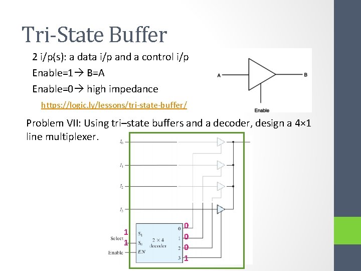
Tri-State Buffer 2 i/p(s): a data i/p and a control i/p Enable=1 B=A Enable=0 high impedance https: //logic. ly/lessons/tri-state-buffer/ Problem VII: Using tri–state buffers and a decoder, design a 4× 1 line multiplexer. 1 1 0 0 0 1

On-Line Challenge Assignment • Design a 3 -input XOR function using MUX only Stay Safe Eng. Minar El-Aasser minar. elaasser@guc. edu. eg