Chap 8 IntegratedCircuit Logic Families n 8 1

- Slides: 62
Chap. 8 Integrated-Circuit Logic Families n 8 -1 Chapter Outcomes (Objectives) u Read and understand digital IC terminology as specified in manufacturers’ u u u u u Digital Systems data sheets. Compare the characteristics of standard TTL and the various TTL series. Determine the fan-out for a particular logic device. Use logic devices with open-collector outputs. Analyze circuits containing tristate devices. Compare the characteristics of the various CMOS series. Analyze circuits that use a CMOS bilateral switch to allow a digital system to control analog signals. Describe the major characteristics of and differences among TTL, ECL, MOS, and CMOS logic families. Describe the various considerations that are required when interfacing digital circuits from different logic families. Use voltage comparators to allow a digital system to be controlled by analog signals. Use a logic pulser and a logic probe as digital circuit troubleshooting tools. Chap. 8 Integrated-Circuit Logic Families © Korea Univ. of Tech. & Edu. Dept. of Info. & Comm.
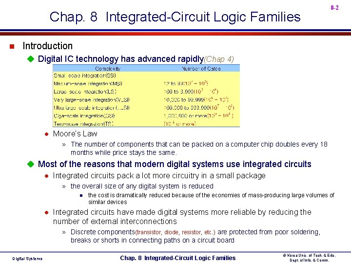
Chap. 8 Integrated-Circuit Logic Families n 8 -2 Introduction u Digital IC technology has advanced rapidly(Chap 4) l Moore’s Law » The number of components that can be packed on a computer chip doubles every 18 months while price stays the same. u Most of the reasons that modern digital systems use integrated circuits l Integrated circuits pack a lot more circuitry in a small package » the overall size of any digital system is reduced n l the cost is dramatically reduced because of the economies of mass-producing large volumes of similar devices Integrated circuits have made digital systems more reliable by reducing the number of external interconnections » Discrete components(transistor, diode, resistor, etc. ) are protected from poor soldering, breaks or shorts in connecting paths on a circuit board Digital Systems Chap. 8 Integrated-Circuit Logic Families © Korea Univ. of Tech. & Edu. Dept. of Info. & Comm.
8 -3 l Integrated circuits have drastically reduced the amount of electrical power needed to perform a given function » Integrated circuitry typically requires less power than their discrete counterparts n n the saving in power supply costs does not require much cooling u There are some things that Integrated Circuits cannot do l Integrated circuits can not handle very large currents or voltages (because the heat generated in such small spaces would cause temperatures to rise beyond acceptable limits) l Integrated circuits can not easily implement certain electrical devices such as inductors, transformers, and large capacitors u For these reason l Integrated circuits are principally used to perform low-power circuit operations that are commonly called information processing l The operations that require high power levels or devices that can not be integrated are still handled by discrete components u Various Logic Families l Bipolar transistors : TTL and ECL l Unipolar MOSFET transistors : NMOS, PMOS, and CMOS Digital Systems Chap. 8 Integrated-Circuit Logic Families * Transistor의 작용은 carrier로서 1) Electron 과 Hole, 모두의 이동 을 이용하는 Bipolar 2) Electron 또는 Hole 중 하나만 의 이동을 이용하는 Unipolar © Korea Univ. of Tech. & Edu. Dept. of Info. & Comm.
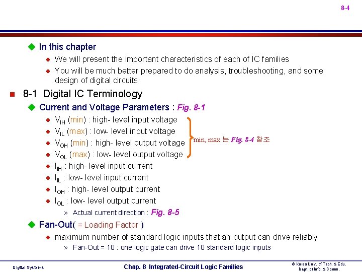
8 -4 u In this chapter l We will present the important characteristics of each of IC families l You will be much better prepared to do analysis, troubleshooting, and some design of digital circuits n 8 -1 Digital IC Terminology u Current and Voltage Parameters : Fig. 8 -1 l VIH (min) : high- level input voltage l VIL (max) : low- level input voltage min, max 는 Fig. 8 -4 참조 l VOH (min) : high- level output voltage l VOL (max) : low- level output voltage l IIH : high- level input current l IIL : low- level input current l IOH : high- level output current l IOL : low- level output current » Actual current direction : Fig. 8 -5 u Fan-Out( = Loading Factor ) l maximum number of standard logic inputs that an output can drive reliably » Fan-Out = 10 : one logic gate can drive 10 standard logic inputs Digital Systems Chap. 8 Integrated-Circuit Logic Families © Korea Univ. of Tech. & Edu. Dept. of Info. & Comm.
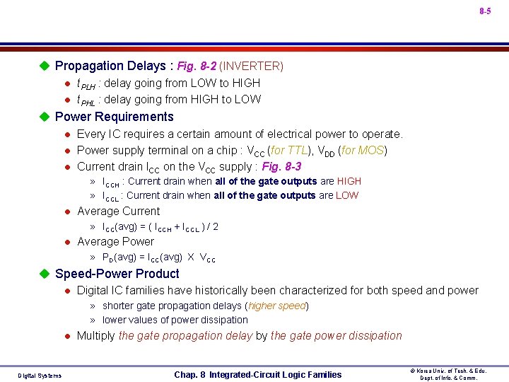
8 -5 u Propagation Delays : Fig. 8 -2 (INVERTER) l t. PLH : delay going from LOW to HIGH l t. PHL : delay going from HIGH to LOW u Power Requirements l Every IC requires a certain amount of electrical power to operate. l Power supply terminal on a chip : VCC (for TTL), VDD (for MOS) l Current drain ICC on the VCC supply : Fig. 8 -3 » ICCH : Current drain when all of the gate outputs are HIGH » ICCL : Current drain when all of the gate outputs are LOW l Average Current » ICC(avg) = ( ICCH + ICCL ) / 2 l Average Power » PD(avg) = ICC(avg) X VCC u Speed-Power Product l Digital IC families have historically been characterized for both speed and power » shorter gate propagation delays (higher speed) » lower values of power dissipation l Digital Systems Multiply the gate propagation delay by the gate power dissipation Chap. 8 Integrated-Circuit Logic Families © Korea Univ. of Tech. & Edu. Dept. of Info. & Comm.
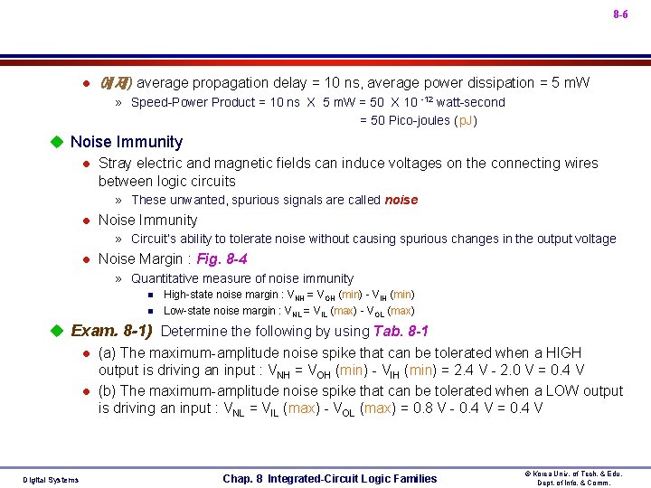
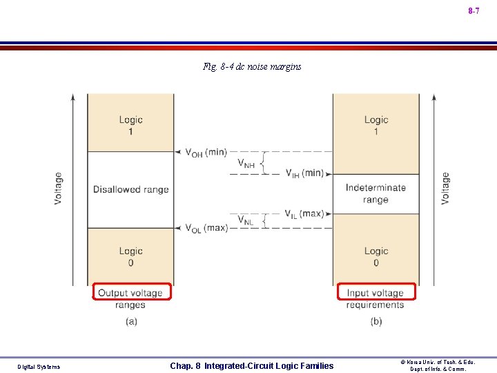
8 -6 l 예제) average propagation delay = 10 ns, average power dissipation = 5 m. W » Speed-Power Product = 10 ns X 5 m. W = 50 X 10 -12 watt-second = 50 Pico-joules (p. J) u Noise Immunity l Stray electric and magnetic fields can induce voltages on the connecting wires between logic circuits » These unwanted, spurious signals are called noise l Noise Immunity » Circuit’s ability to tolerate noise without causing spurious changes in the output voltage l Noise Margin : Fig. 8 -4 » Quantitative measure of noise immunity n n High-state noise margin : VNH = VOH (min) - VIH (min) Low-state noise margin : VNL = VIL (max) - VOL (max) u Exam. 8 -1) Determine the following by using Tab. 8 -1 l (a) The maximum-amplitude noise spike that can be tolerated when a HIGH output is driving an input : VNH = VOH (min) - VIH (min) = 2. 4 V - 2. 0 V = 0. 4 V l (b) The maximum-amplitude noise spike that can be tolerated when a LOW output is driving an input : VNL = VIL (max) - VOL (max) = 0. 8 V - 0. 4 V = 0. 4 V Digital Systems Chap. 8 Integrated-Circuit Logic Families © Korea Univ. of Tech. & Edu. Dept. of Info. & Comm.
8 -7 • Fig. 8 -4 dc noise margins Digital Systems Chap. 8 Integrated-Circuit Logic Families © Korea Univ. of Tech. & Edu. Dept. of Info. & Comm.
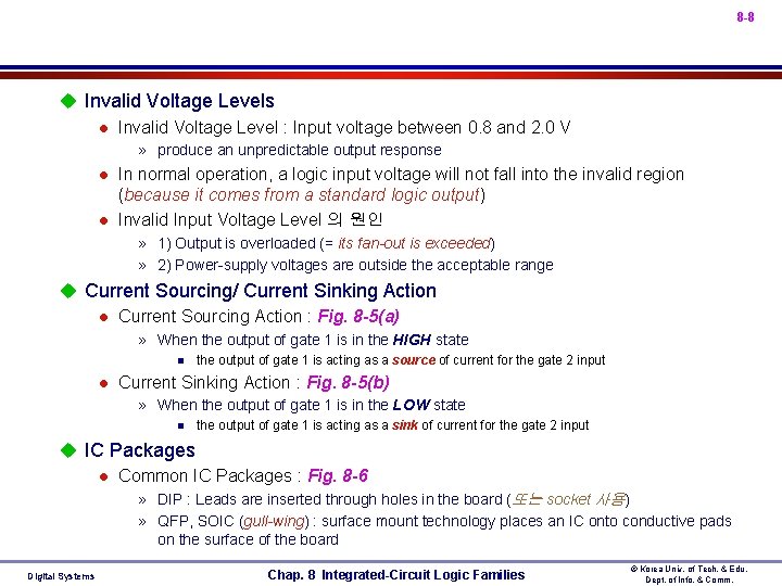
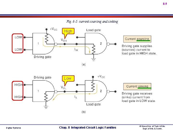
8 -8 u Invalid Voltage Levels l Invalid Voltage Level : Input voltage between 0. 8 and 2. 0 V » produce an unpredictable output response l l In normal operation, a logic input voltage will not fall into the invalid region (because it comes from a standard logic output) Invalid Input Voltage Level 의 원인 » 1) Output is overloaded (= its fan-out is exceeded) » 2) Power-supply voltages are outside the acceptable range u Current Sourcing/ Current Sinking Action l Current Sourcing Action : Fig. 8 -5(a) » When the output of gate 1 is in the HIGH state n l the output of gate 1 is acting as a source of current for the gate 2 input Current Sinking Action : Fig. 8 -5(b) » When the output of gate 1 is in the LOW state n the output of gate 1 is acting as a sink of current for the gate 2 input u IC Packages l Common IC Packages : Fig. 8 -6 » DIP : Leads are inserted through holes in the board (또는 socket 사용) » QFP, SOIC (gull-wing) : surface mount technology places an IC onto conductive pads on the surface of the board Digital Systems Chap. 8 Integrated-Circuit Logic Families © Korea Univ. of Tech. & Edu. Dept. of Info. & Comm.
8 -9 • Fig. 8 -5 current sourcing and sinking High Low Digital Systems Chap. 8 Integrated-Circuit Logic Families © Korea Univ. of Tech. & Edu. Dept. of Info. & Comm.
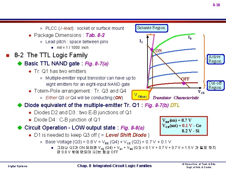
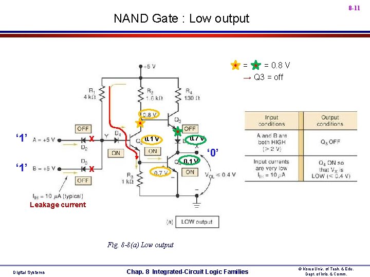
8 -10 Saturate Region » PLCC (J-lead) : socket or surface mount l Package Dimensions : Tab. 8 -2 » Lead pitch : space between pins n n IB IC mil = 1 / 1000 inch ON 8 -2 The TTL Logic Family Active Region u Basic TTL NAND gate : Fig. 8 -7(a) l Tr. Q 1 has two emitters » Multiple-emitter input transistor can have up to eight emitters for an eight-input NAND gate l Totem-Pole arrangement : Tr. Q 3 and Q 4 » Either Q 3 or Q 4 will be conducting (ON) VCE(sat) OFF VCE Cut-off Region Transistor Characteristic u Diode equivalent of the multiple-emitter Tr. Q 1 : Fig. 8 -7(b) DTL l Diodes D 2 and D 3 : two E-B junctions of Q 1 l Diode D 4 : C-B junction of Q 1 VBE(on) = 0. 7 V u Circuit Operation - LOW output state : Fig. 8 -8(a) l D 1 is needed to keep Q 3 off ( = Level Shift Diode ) VCE(sat) = 0. 1 V - Ge 0. 2 V - Si » Base Voltage (Q 3) = 0. 8 V = VBE (Q 4) + VCE (Q 2) = 0. 7 V + 0. 1 V n Digital Systems 그러나 Q 3가 ON 되려면 VCE (Q 4) + VD 1 + VBE (Q 3) = 0. 1 V + 0. 7 V = 1. 5 V 가 필요 하지 만 0. 8 V 밖에 안되어 Q 3는 항상 OFF Chap. 8 Integrated-Circuit Logic Families © Korea Univ. of Tech. & Edu. Dept. of Info. & Comm.
• NAND Gate : Low output 8 -11 • = = 0. 8 V • → Q 3 = off • ‘ 1’ x • 0. 1 V • 0. 7 V • 0. 1 V x • ‘ 0’ • Leakage current • Fig. 8 -8(a) Low output Digital Systems Chap. 8 Integrated-Circuit Logic Families © Korea Univ. of Tech. & Edu. Dept. of Info. & Comm.
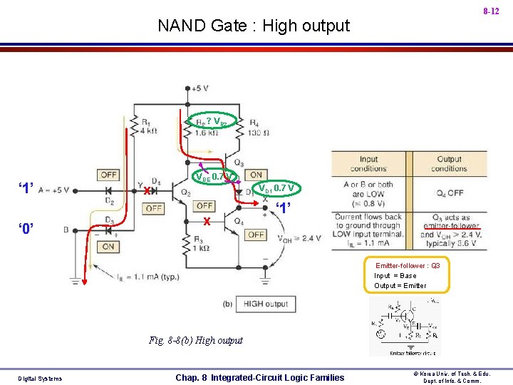
8 -12 • NAND Gate : High output • ? VR 2 • ‘ 1’ • ‘ 0’ x • VBE 0. 7 V • VD 1 0. 7 V x • ‘ 1’ Emitter-follower : Q 3 -Input = Base -Output = Emitter • Fig. 8 -8(b) High output Digital Systems Chap. 8 Integrated-Circuit Logic Families © Korea Univ. of Tech. & Edu. Dept. of Info. & Comm.
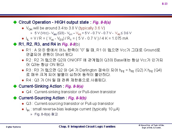
8 -13 u Circuit Operation - HIGH output state : Fig. 8 -8(a) l VOH will be around 3. 4 to 3. 8 V (typically 3. 6 V) » 5 V (Vcc) - VBE (Q 3) - VD 1 – VR 2 = 5 V - 0. 7 V - VR 2 3. 6 V l IIL = V / R = ( Vcc - VD 3) / R 1 = ( 5 V - 0. 7 V ) / 4 K = 1. 075 m. A u R 1, R 2, R 3, and R 4 in Fig. 8 -8(b) l R 1 : A 와 B 중에서 어느 한쪽이 “ 0” 일 때, R 1 이 없으면 Vcc가 그대로 Ground로 연결되어 전원이 Short 된다 l R 2 : R 2 가 없으면 Q 2의 ON/OFF 에 관계없이 Q 3의 Base에는 항상 Vcc가 인가되 어 Q 3는 항상 ON 된다. l R 3 : R 3 가 없으면 Q 2 와 Q 4 가 Darlington 접속이 되어 h. FE = h. FE (Q 2) X h. FE (Q 4) 로 매우 크게 되어 발열이 심하여 동작이 불안하다. l R 4 : Q 3 가 ON 일 때 전류 제한용으로 사용된다. u Current-Sinking Action : Fig. 8 -9(a) l Q 4 : Current-sinking transistor or Pull-down transistor u Current-Sourcing Action : Fig. 8 -9(b) l Q 3 : Current-sourcing transistor or Pull-up transistor l IIH : small reverse-bias leakage current (typically 10 A) » Fig. 8 -8(a) 참고 Digital Systems Chap. 8 Integrated-Circuit Logic Families © Korea Univ. of Tech. & Edu. Dept. of Info. & Comm.
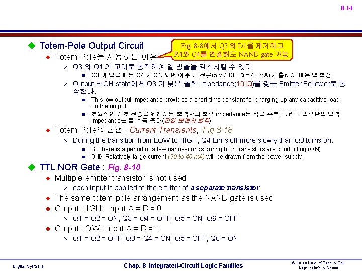
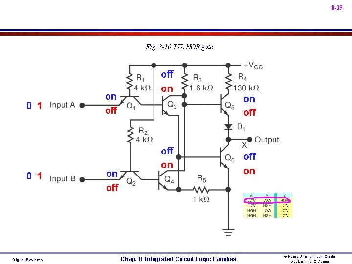
8 -14 u Totem-Pole Output Circuit l Totem-Pole을 사용하는 이유 Fig. 8 -8에서 Q 3 와 D 1을 제거하고 R 4와 Q 4를 연결해도 NAND gate 가능 » Q 3 와 Q 4 가 교대로 동작하여 열 방출을 감소시킬 수 있다. n Q 3 가 없을 때는 Q 4 가 ON 되면 아주 큰 전류(5 V / 130 = 40 m. A)가 흘러서 많은 열 발생. » Output HIGH state에서 Q 3 가 낮은 출력 Impedance(10 )를 갖는 Emitter Follower로 동 작한다. n n l This low output impedance provides a short time constant for charging up any capacitive load on the output 효율적인 신호 전송을 위해서는 출력단의 출력 impedance는 적을 수록, 그리고 입력단의 입력 impedance는 클 수록 좋다(전압 분배의 법칙). Totem-Pole의 단점 : Current Transients, Fig 8 -18 » During the transition from LOW to HIGH, Q 4 turns off more slowly than Q 3 turns on. n n So there is a period of a few nanoseconds during both transistors are conducting (ON) 이때 Relatively large current (30 to 40 m. A) will be drawn from the power supply. u TTL NOR Gate : Fig. 8 -10 l Multiple-emitter transistor is not used » each input is applied to the emitter of a separate transistor l l The same totem-pole arrangement as the NAND gate is used Output HIGH : Input A = B = 0 » Q 1 = Q 2 = ON, Q 3 = Q 4 = OFF, Q 5 = ON, Q 6 = OFF l Output LOW : Input A = B = 1 » Q 1 = Q 2 = OFF, Q 3 = Q 4 = ON, Q 5 = OFF, Q 6 = ON Digital Systems Chap. 8 Integrated-Circuit Logic Families © Korea Univ. of Tech. & Edu. Dept. of Info. & Comm.
8 -15 • Fig. 8 -10 TTL NOR gate • 0 1 Digital Systems • on • off • on Chap. 8 Integrated-Circuit Logic Families • on • off • on © Korea Univ. of Tech. & Edu. Dept. of Info. & Comm.
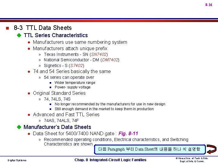
8 -16 n 8 -3 TTL Data Sheets u TTL Series Characteristics l Manufacturers use same numbering system l Manufacturers attach unique prefix » Texas Instruments - SN (SN 7402) » National Semiconductor - DM (DM 7402) » Signetics - S (S 7402) l 74 and 54 Series basically the same » 54 series can operate over n n l Wider temperature range Power- supply voltage Original Standard Series » 74, 74 LS, 74 S n n l No longer recommended by the manufacturers for use in new design Still enough demand in the market to keep them in production Advanced and Fast TTL Series » 74 AS, 74 ALS, 74 F u Manufacturer’s Data Sheets l Data Sheet for 5400/7400 NAND gate : Fig. 8 -11 » Recommended operating conditions, Electrical characteristics, and Switching Characteristics are shown 다음 Paragraph 부터 Data Sheet의 내용을 하나 씩 설명함 Digital Systems Chap. 8 Integrated-Circuit Logic Families © Korea Univ. of Tech. & Edu. Dept. of Info. & Comm.
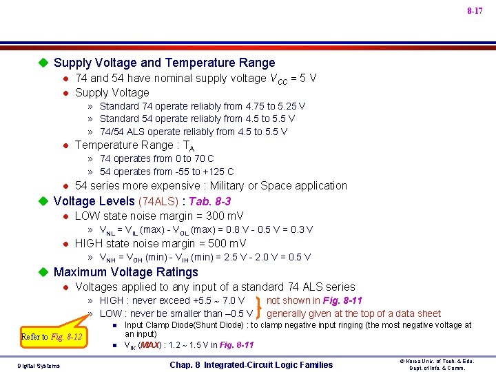
8 -17 u Supply Voltage and Temperature Range l 74 and 54 have nominal supply voltage VCC = 5 V l Supply Voltage » Standard 74 operate reliably from 4. 75 to 5. 25 V » Standard 54 operate reliably from 4. 5 to 5. 5 V » 74/54 ALS operate reliably from 4. 5 to 5. 5 V l Temperature Range : TA » 74 operates from 0 to 70 C » 54 operates from -55 to +125 C 54 series more expensive : Military or Space application u Voltage Levels (74 ALS) : Tab. 8 -3 l LOW state noise margin = 300 m. V l » VNL = VIL (max) - VOL (max) = 0. 8 V - 0. 5 V = 0. 3 V l HIGH state noise margin = 500 m. V » VNH = VOH (min) - VIH (min) = 2. 5 V - 2. 0 V = 0. 5 V u Maximum Voltage Ratings l Voltages applied to any input of a standard 74 ALS series » HIGH : never exceed +5. 5 7. 0 V » LOW : never be smaller than – 0. 5 V n Refer to Fig. 8 -12 n Digital Systems not shown in Fig. 8 -11 generally given at the top of a data sheet Input Clamp Diode(Shunt Diode) : to clamp negative input ringing (the most negative voltage at an input) VIK (MAX) : 1. 2 1. 5 V in Fig. 8 -11 Chap. 8 Integrated-Circuit Logic Families © Korea Univ. of Tech. & Edu. Dept. of Info. & Comm.
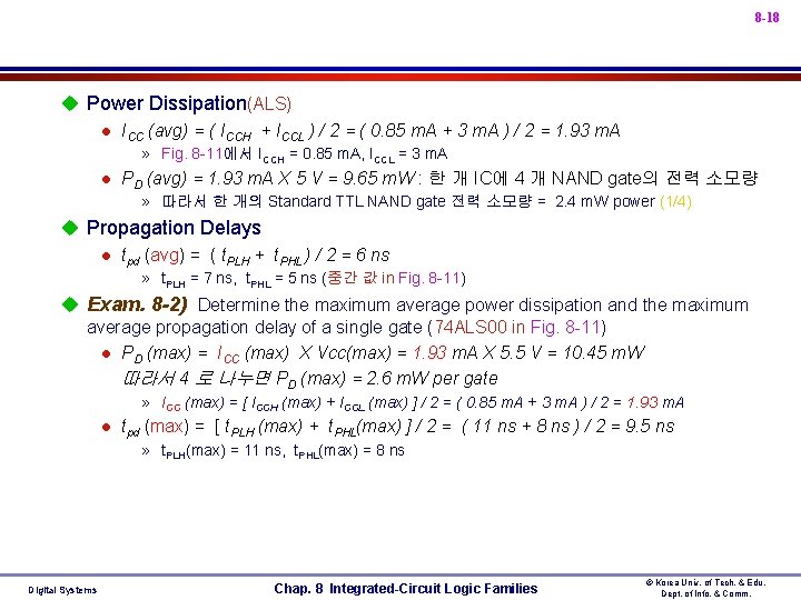
8 -18 u Power Dissipation(ALS) l ICC (avg) = ( ICCH + ICCL ) / 2 = ( 0. 85 m. A + 3 m. A ) / 2 = 1. 93 m. A » Fig. 8 -11에서 ICCH = 0. 85 m. A, ICCL = 3 m. A l PD (avg) = 1. 93 m. A X 5 V = 9. 65 m. W : 한 개 IC에 4 개 NAND gate의 전력 소모량 » 따라서 한 개의 Standard TTL NAND gate 전력 소모량 = 2. 4 m. W power (1/4) u Propagation Delays l tpd (avg) = ( t. PLH + t. PHL ) / 2 = 6 ns » t. PLH = 7 ns, t. PHL = 5 ns (중간 값 in Fig. 8 -11) u Exam. 8 -2) Determine the maximum average power dissipation and the maximum average propagation delay of a single gate (74 ALS 00 in Fig. 8 -11) l PD (max) = ICC (max) X Vcc(max) = 1. 93 m. A X 5. 5 V = 10. 45 m. W 따라서 4 로 나누면 PD (max) = 2. 6 m. W per gate » ICC (max) = [ ICCH (max) + ICCL (max) ] / 2 = ( 0. 85 m. A + 3 m. A ) / 2 = 1. 93 m. A l tpd (max) = [ t. PLH (max) + t. PHL(max) ] / 2 = ( 11 ns + 8 ns ) / 2 = 9. 5 ns » t. PLH(max) = 11 ns, t. PHL(max) = 8 ns Digital Systems Chap. 8 Integrated-Circuit Logic Families © Korea Univ. of Tech. & Edu. Dept. of Info. & Comm.
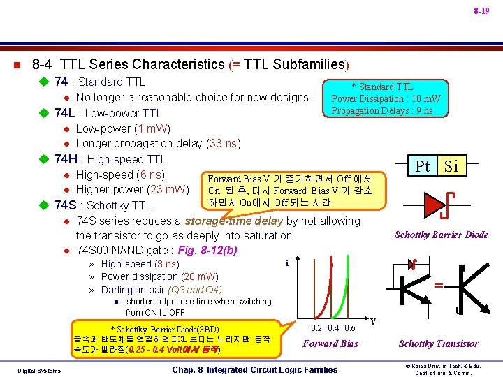
8 -19 n 8 -4 TTL Series Characteristics (= TTL Subfamilies) u 74 : Standard TTL * Standard TTL l No longer a reasonable choice for new designs Power Dissipation : 10 m. W Propagation Delays : 9 ns u 74 L : Low-power TTL l Low-power (1 m. W) l Longer propagation delay (33 ns) u 74 H : High-speed TTL Pt Si l High-speed (6 ns) Forward Bias V 가 증가하면서 Off 에서 l Higher-power (23 m. W) On 된 후, 다시 Forward Bias V 가 감소 하면서 On에서 Off 되는 시간 u 74 S : Schottky TTL l 74 S series reduces a storage-time delay by not allowing Schottky Barrier Diode the transistor to go as deeply into saturation l 74 S 00 NAND gate : Fig. 8 -12(b) » High-speed (3 ns) » Power dissipation (20 m. W) » Darlington pair (Q 3 and Q 4) n = shorter output rise time when switching from ON to OFF * Schottky Barrier Diode(SBD) 금속과 반도체를 연결하면 ECL 보다는 느리지만 동작 속도가 빨라짐(0. 25 - 0. 4 Volt에서 동작) Digital Systems i 0. 2 0. 4 0. 6 Forward Bias Chap. 8 Integrated-Circuit Logic Families V Schottky Transistor © Korea Univ. of Tech. & Edu. Dept. of Info. & Comm.
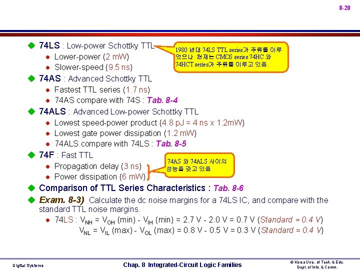
8 -20 u 74 LS : Low-power Schottky TTL 1980 년대 74 LS TTL series가 주류를 이루 었으나 현재는 CMOS series 74 HC 와 l Lower-power (2 m. W) 74 HCT series가 주류를 이루고 있음. l Slower-speed (9. 5 ns) u 74 AS : Advanced Schottky TTL l Fastest TTL series (1. 7 ns) l 74 AS compare with 74 S : Tab. 8 -4 u 74 ALS : Advanced Low-power Schottky TTL l Lowest speed-power product (4. 8 p. J = 4 ns x 1. 2 m. W) l Lowest gate power dissipation (1. 2 m. W) l 74 ALS compare with 74 LS : Tab. 8 -5 u 74 F : Fast TTL 74 AS 와 74 ALS 사이의 l Propagation delay (3 ns) 성능을 갖고 있음 l Power dissipation (6 m. W) u Comparison of TTL Series Characteristics : Tab. 8 -6 u Exam. 8 -3) Calculate the dc noise margins for a 74 LS IC, and compare with the standard TTL noise margins. l 74 LS : VNH = VOH (min) - VIH (min) = 2. 7 V - 2. 0 V = 0. 7 V (Standard = 0. 4 V) VNL = VIL (max) - VOL (max) = 0. 8 V - 0. 5 V = 0. 3 V (Standard = 0. 4 V) Digital Systems Chap. 8 Integrated-Circuit Logic Families © Korea Univ. of Tech. & Edu. Dept. of Info. & Comm.
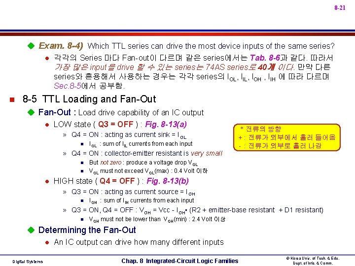
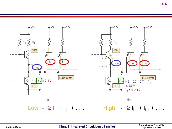
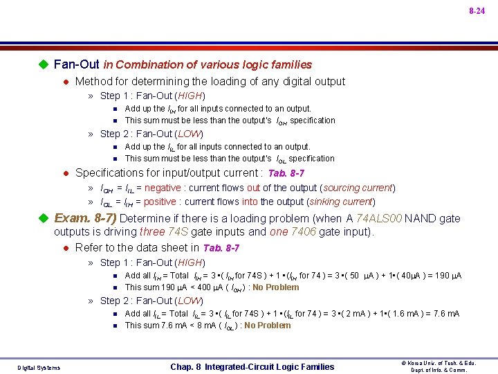
8 -21 u Exam. 8 -4) Which TTL series can drive the most device inputs of the same series? l 각각의 Series 마다 Fan-out이 다르며 같은 series에서는 Tab. 8 -6과 같다. 따라서 가장 많은 input을 drive 할 수 있는 series는 74 AS series로 40개 이다. 만약 다른 series와 혼용해서 사용하는 경우는 각각 series의 IOL, IIL, IOH , IIH 에 따라 다르며 Sec. 8 -5에서 공부함. n 8 -5 TTL Loading and Fan-Out u Fan-Out : Load drive capability of an IC output l LOW state ( Q 3 = OFF ) : Fig. 8 -13(a) » Q 4 = ON : acting as current sink = IOL n IOL : sum of IIL currents from each input » Q 4 = ON : collector-emitter resistant is very small n n l * 전류의 방향 + : 전류가 외부에서 흘러 들어옴 - : 전류가 외부로 흘러 나감 But not zero : produce a voltage drop VOL must not exceed VOL(max) : 0. 4 Volt 이하 HIGH state ( Q 4 = OFF ) : Fig. 8 -13(b) » Q 3 = ON : acting as current source = IOH n IOH : sum of IIH currents from each input » Q 3 = ON, Q 4 = OFF : VOH = Vcc - IOH • (R 2 + emitter-base resistant + D 1 resistant) n VOH must not be lower than VOH(min) : 2. 4 Volt 이상 u Determining the Fan-Out l An IC output can drive how many different inputs Digital Systems Chap. 8 Integrated-Circuit Logic Families © Korea Univ. of Tech. & Edu. Dept. of Info. & Comm.
8 -22 • 0. 7 V • 0. 1 V • ≤ 0. 4 V • = 5 – 0. 7 – VR 2 • ≤ 3. 6 V • Typ. ≥ 2. 4 V • Low IOL ≥ IIL + …. . Digital Systems • High IOH ≥ IIH + …. . Chap. 8 Integrated-Circuit Logic Families © Korea Univ. of Tech. & Edu. Dept. of Info. & Comm.
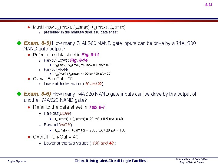
8 -23 l Must Know IOL(max), IOH(max), IIL (max) , IIH (max) » presented in the manufacturer’s IC data sheet u Exam. 8 -5) How many 74 ALS 00 NAND gate inputs can be drive by a 74 ALS 00 NAND gate output? l Refer to the data sheet in Fig. 8 -11 » Fan-out(LOW) : Fig. 8 -14 n IOL(max) / IIL (max) = 8 m. A / 0. 1 m. A = 80 » Fan-out(HIGH) n l IOH(max) / IIH (max) = 400 A / 20 A = 20 Overall Fan-Out = 20 » Lower of the two values ( 80 and 20 ) u Exam. 8 -6) How many 74 AS 20 NAND gate inputs can be drive by the output of another 74 AS 20 NAND gate? l Refer to the data sheet in Tab. 8 -7 » Fan-out(LOW) n IOL(max) / IIL (max) = 20 m. A / 0. 5 m. A = 40 » Fan-out(HIGH) n l IOH(max) / IIH (max) = 2000 A / 20 A = 100 Overall Fan-Out = 40 » Lower of the two values ( 100 and 40 ) Digital Systems Chap. 8 Integrated-Circuit Logic Families © Korea Univ. of Tech. & Edu. Dept. of Info. & Comm.
8 -24 u Fan-Out in Combination of various logic families l Method for determining the loading of any digital output » Step 1 : Fan-Out (HIGH) n n Add up the IIH for all inputs connected to an output. This sum must be less than the output’s IOH specification » Step 2 : Fan-Out (LOW) n n l Add up the IIL for all inputs connected to an output. This sum must be less than the output’s IOL specification Specifications for input/output current : Tab. 8 -7 » IOH = IIL = negative : current flows out of the output (sourcing current) » IOL = IIH = positive : current flows into the output (sinking current) u Exam. 8 -7) Determine if there is a loading problem (when A 74 ALS 00 NAND gate outputs is driving three 74 S gate inputs and one 7406 gate input). l Refer to the data sheet in Tab. 8 -7 » Step 1 : Fan-Out (HIGH) n n Add all IIH = Total IIH = 3 • ( IIH for 74 S ) + 1 • (IIH for 74 ) = 3 • ( 50 A ) + 1 • ( 40 A ) = 190 A This sum 190 A < 400 A ( IOH ) : No Problem » Step 2 : Fan-Out (LOW) n n Digital Systems Add all IIL = Total IIL = 3 • ( IIL for 74 S ) + 1 • (IIL for 74 ) = 3 • ( 2 m. A ) + 1 • ( 1. 6 m. A ) = 7. 6 m. A This sum 7. 6 m. A < 8 m. A ( IOL ) : No Problem Chap. 8 Integrated-Circuit Logic Families © Korea Univ. of Tech. & Edu. Dept. of Info. & Comm.
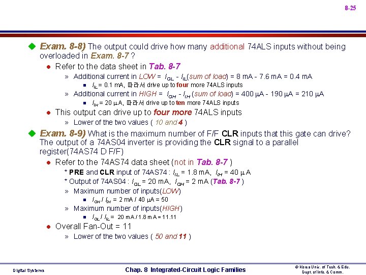
8 -25 u Exam. 8 -8) The output could drive how many additional 74 ALS inputs without being overloaded in Exam. 8 -7 ? l Refer to the data sheet in Tab. 8 -7 » Additional current in LOW = IOL - IIL(sum of load) = 8 m. A - 7. 6 m. A = 0. 4 m. A n IIL = 0. 1 m. A, 따라서 drive up to four more 74 ALS inputs » Additional current in HIGH = IOH - IIH (sum of load) = 400 A - 190 A = 210 A n l IIH = 20 A, 따라서 drive up to ten more 74 ALS inputs This output can drive up to four more 74 ALS inputs » Lower of the two values ( 10 and 4 ) u Exam. 8 -9) What is the maximum number of F/F CLR inputs that this gate can drive? The output of a 74 AS 04 inverter is providing the CLR signal to a parallel register(74 AS 74 D F/F) l Refer to the 74 AS 74 data sheet (not in Tab. 8 -7 ) * PRE and CLR input of 74 AS 74 : IIL = 1. 8 m. A, IIH = 40 A * Output of 74 AS 04 : IOL = 20 m. A, IOH = 2 m. A (Tab. 8 -7 ) » Maximum number of inputs(LOW) n IOH / IIH = 2 m. A / 40 A = 50 » Maximum number of inputs(HIGH) n l IOL / IIL = 20 m. A / 1. 8 m. A = 11. 11 Overall Fan-Out = 11 » Lower of the two values ( 50 and 11 ) Digital Systems Chap. 8 Integrated-Circuit Logic Families © Korea Univ. of Tech. & Edu. Dept. of Info. & Comm.
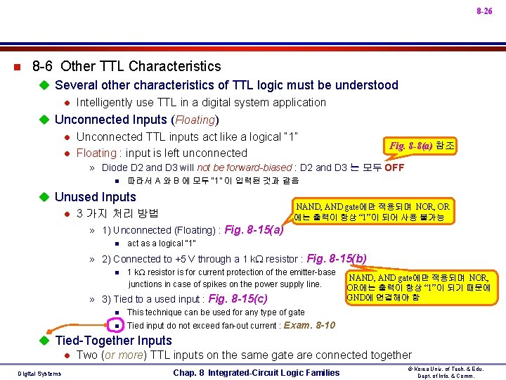
8 -26 n 8 -6 Other TTL Characteristics u Several other characteristics of TTL logic must be understood l Intelligently use TTL in a digital system application u Unconnected Inputs (Floating) l Unconnected TTL inputs act like a logical “ 1” l Floating : input is left unconnected Fig. 8 -8(a) 참조 » Diode D 2 and D 3 will not be forward-biased : D 2 and D 3 는 모두 OFF n 따라서 A 와 B 에 모두 “ 1” 이 입력된 것과 같음 u Unused Inputs l 3 가지 처리 방법 NAND, AND gate에만 적용되며 NOR, OR 에는 출력이 항상 “ 1”이 되어 사용 불가능 » 1) Unconnected (Floating) : Fig. 8 -15(a) n act as a logical “ 1” » 2) Connected to +5 V through a 1 k resistor : Fig. 8 -15(b) n 1 k resistor is for current protection of the emitter-base junctions in case of spikes on the power supply line. » 3) Tied to a used input : Fig. 8 -15(c) n This technique can be used for any type of gate n Tied input do not exceed fan-out current : Exam. 8 -10 NAND, AND gate에만 적용되며 NOR, OR에는 출력이 항상 “ 1”이 되기 때문에 GND에 연결해야 함 u Tied-Together Inputs l Two (or more) TTL inputs on the same gate are connected together Digital Systems Chap. 8 Integrated-Circuit Logic Families © Korea Univ. of Tech. & Edu. Dept. of Info. & Comm.
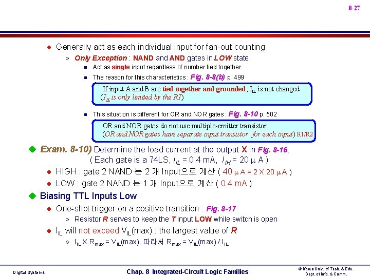
8 -27 l Generally act as each individual input for fan-out counting » Only Exception : NAND and AND gates in LOW state n Act as single input regardless of number tied together n The reason for this characteristics : Fig. 8 -8(b) p. 499 If input A and B are tied together and grounded, IIL is not changed (IIL is only limited by the R 1) n This situation is different for OR and NOR gates : Fig. 8 -10 p. 502 OR and NOR gates do not use multiple-emitter transistor (OR and NOR gates have separate input transistor for each input) R 1/R 2 u Exam. 8 -10) Determine the load current at the output X in Fig. 8 -16. ( Each gate is a 74 LS, IIL = 0. 4 m. A, IIH = 20 A ) l HIGH : gate 2 NAND 는 2 개 Input으로 계산 ( 40 A = 2 X 20 A ) l LOW : gate 2 NAND 는 1 개 Input으로 계산 ( 0. 4 m. A ) u Biasing TTL Inputs Low l One-shot trigger on a positive transition : Fig. 8 -17 » Resistor R serves to keep the T input LOW while switch is open l IIL will not exceed VIL(max) : the largest value of R » IIL X Rmax = VIL(max), 따라서 Rmax = VIL(max) / IIL Digital Systems Chap. 8 Integrated-Circuit Logic Families © Korea Univ. of Tech. & Edu. Dept. of Info. & Comm.
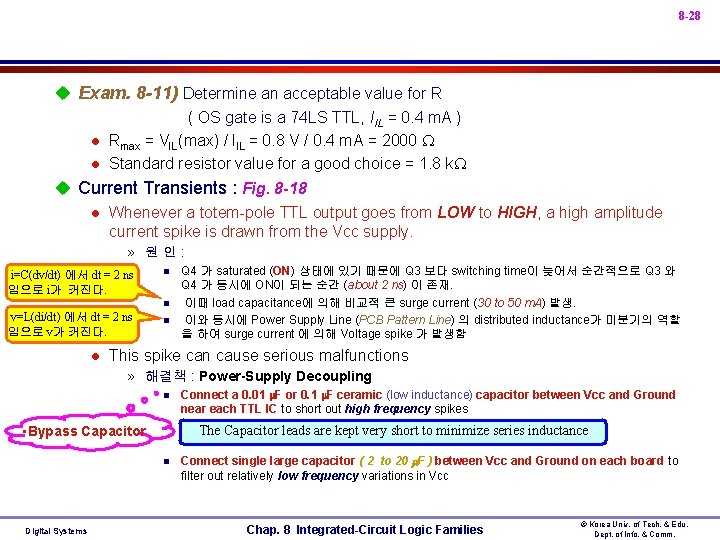
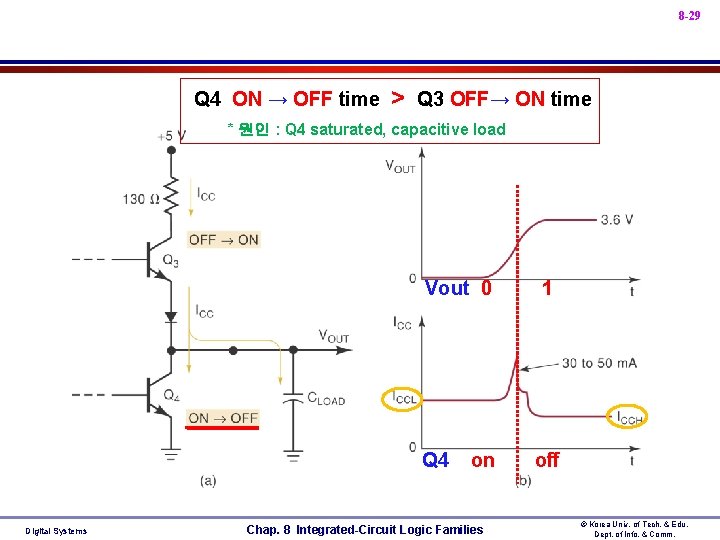
8 -28 u Exam. 8 -11) Determine an acceptable value for R ( OS gate is a 74 LS TTL, IIL = 0. 4 m. A ) l Rmax = VIL(max) / IIL = 0. 8 V / 0. 4 m. A = 2000 l Standard resistor value for a good choice = 1. 8 k u Current Transients : Fig. 8 -18 l Whenever a totem-pole TTL output goes from LOW to HIGH, a high amplitude current spike is drawn from the Vcc supply. » 원인: i=C(dv/dt) 에서 dt = 2 ns 임으로 i가 커진다. n n v=L(di/dt) 에서 dt = 2 ns 임으로 v가 커진다. l n Q 4 가 saturated (ON) 상태에 있기 때문에 Q 3 보다 switching time이 늦어서 순간적으로 Q 3 와 Q 4 가 동시에 ON이 되는 순간 (about 2 ns) 이 존재. 이때 load capacitance에 의해 비교적 큰 surge current (30 to 50 m. A) 발생. 이와 동시에 Power Supply Line (PCB Pattern Line) 의 distributed inductance가 미분기의 역할 을 하여 surge current 에 의해 Voltage spike 가 발생함 This spike can cause serious malfunctions » 해결책 : Power-Supply Decoupling n The Capacitor leads are kept very short to minimize series inductance • Bypass Capacitor n Digital Systems Connect a 0. 01 F or 0. 1 F ceramic (low inductance) capacitor between Vcc and Ground near each TTL IC to short out high frequency spikes Connect single large capacitor ( 2 to 20 F ) between Vcc and Ground on each board to filter out relatively low frequency variations in Vcc Chap. 8 Integrated-Circuit Logic Families © Korea Univ. of Tech. & Edu. Dept. of Info. & Comm.
8 -29 • Q 4 ON → OFF time > Q 3 OFF→ ON time • * 원인 : Q 4 saturated, capacitive load • Vout 0 • Q 4 Digital Systems on Chap. 8 Integrated-Circuit Logic Families 1 off © Korea Univ. of Tech. & Edu. Dept. of Info. & Comm.
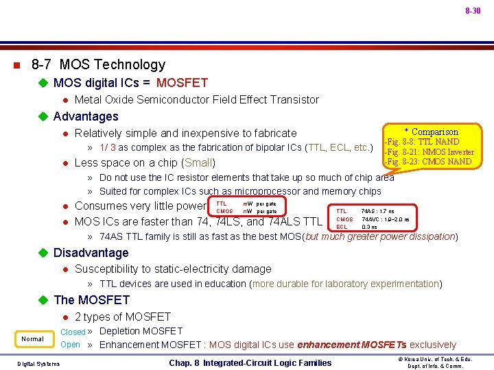
8 -30 n 8 -7 MOS Technology u MOS digital ICs = MOSFET l Metal Oxide Semiconductor Field Effect Transistor u Advantages l Relatively simple and inexpensive to fabricate * Comparison » 1/ 3 as complex as the fabrication of bipolar ICs (TTL, ECL, etc. ) l Less space on a chip (Small) -Fig. 8 -8: TTL NAND -Fig. 8 -21: NMOS Inverter -Fig. 8 -23: CMOS NAND » Do not use the IC resistor elements that take up so much of chip area » Suited for complex ICs such as microprocessor and memory chips l l m. W per gate Consumes very little power • • TTL CMOS n. W per gate MOS ICs are faster than 74, 74 LS, and 74 ALS TTL • TTL • CMOS • ECL 74 AS : 1. 7 ns 74 AVC : 1. 9~2. 0 ns 0. 3 ns » 74 AS TTL family is still as fast as the best MOS(but much greater power dissipation) u Disadvantage l Susceptibility to static-electricity damage » TTL devices are used in education (more durable for laboratory experimentation) u The MOSFET l 2 types of MOSFET Normal Digital Systems Closed » Depletion MOSFET Open » Enhancement MOSFET : MOS digital ICs use enhancement MOSFETs exclusively Chap. 8 Integrated-Circuit Logic Families © Korea Univ. of Tech. & Edu. Dept. of Info. & Comm.
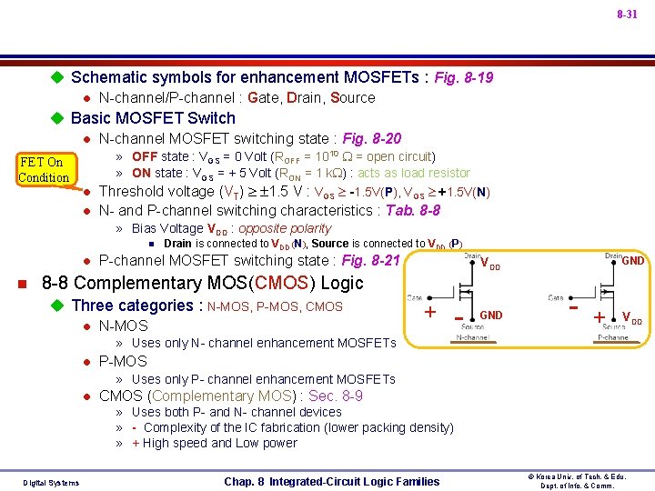
8 -31 u Schematic symbols for enhancement MOSFETs : Fig. 8 -19 l N-channel/P-channel : Gate, Drain, Source u Basic MOSFET Switch l N-channel MOSFET switching state : Fig. 8 -20 FET On Condition » OFF state : VGS = 0 Volt (ROFF = 1010 = open circuit) » ON state : VGS = + 5 Volt (RON = 1 k ) : acts as load resistor l Threshold voltage (VT) 1. 5 V : VGS -1. 5 V(P), VGS +1. 5 V(N) l N- and P-channel switching characteristics : Tab. 8 -8 » Bias Voltage VDD : opposite polarity n l n Drain is connected to VDD (N), Source is connected to VDD (P) P-channel MOSFET switching state : Fig. 8 -21 8 -8 Complementary MOS(CMOS) Logic u Three categories : N-MOS, P-MOS, CMOS l N-MOS • GND • VDD • + • - • GND • - • + • VDD » Uses only N- channel enhancement MOSFETs l P-MOS » Uses only P- channel enhancement MOSFETs l CMOS (Complementary MOS) : Sec. 8 -9 » Uses both P- and N- channel devices » - Complexity of the IC fabrication (lower packing density) » + High speed and Low power Digital Systems Chap. 8 Integrated-Circuit Logic Families © Korea Univ. of Tech. & Edu. Dept. of Info. & Comm.
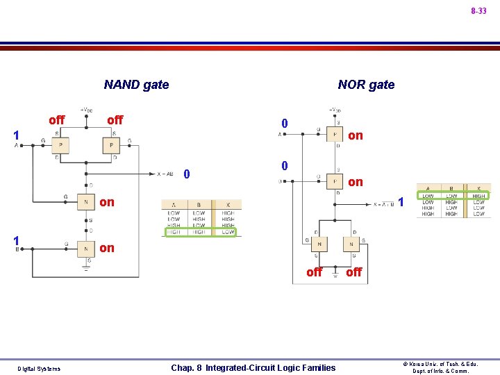
8 -32 u CMOS Inverter : Fig. 8 -22 l VIN = + VDD : VOUT = 0 V » ROFF (Q 1 = OFF) = 1010 » RON (Q 2 = ON) = 1 k l VIN = 0 V : VOUT = + VDD » RON (Q 1 = ON) = 1 k » ROFF (Q 2 = OFF) = 1010 u CMOS NAND gate : Fig. 8 -23 l Both A = B = HIGH, X = LOW » Q 1 = Q 3 = OFF, Q 2 = Q 4 = ON u CMOS NOR gate : Fig. 8 -24 l Both A = B = LOW, X = HIGH » Q 1 = Q 3 = ON, Q 2 = Q 4 = OFF Digital Systems Chap. 8 Integrated-Circuit Logic Families © Korea Univ. of Tech. & Edu. Dept. of Info. & Comm.
8 -33 • NAND gate • off • NOR gate • off • 0 • 1 • 0 • on • 0 • on • 1 • on • off Digital Systems Chap. 8 Integrated-Circuit Logic Families • off © Korea Univ. of Tech. & Edu. Dept. of Info. & Comm.
8 -34 u CMOS Flip-Flops Fig. 5 -6 Fig. 5 -10 l Two CMOS NOR gates or NAND gates can be cross-coupled l Additional gating circuitry (Edge detector/Pulse steering) is used : Fig. 5 -25(p. 229) n 8 -9 CMOS Series Characteristics u Compared with TTL l Slower l Lower power l Better noise margin l Greater supply voltage range l Higher fan-out l More dense u Replacement Rules for Different Families/Series l Pin-compatible » pin configuration must be same (pin 7 = GND, pin 14 = Vcc) l Functionally equivalent » logic function must be same (6 D F/F with positive edge clock) l Electrically compatible » two ICs can be connected directly to each other (without taking any special measures to ensure properation) Digital Systems Chap. 8 Integrated-Circuit Logic Families © Korea Univ. of Tech. & Edu. Dept. of Info. & Comm.
8 -35 u 4000/ 14000 series l Oldest series (RCA) l Very low power dissipation l 3 to 15 V power- supply voltages l Very slow l Very low output current capability l Not pin-compatible with any TTL series l Not electrically-compatible with any TTL series u 74 C series l Pin-compatible and functionally equivalent to TTL with same number l Performance much like 4000 series u 74 HC/ HCT (high- speed CMOS) l 10 times faster than 74 C series l Pin-compatible and functionally equivalent to TTL with same number l 74 HCT devices electrically compatible with TTL l 74 HC devices not electrically compatible with TTL Digital Systems Chap. 8 Integrated-Circuit Logic Families © Korea Univ. of Tech. & Edu. Dept. of Info. & Comm.
8 -36 u 74 AC/ ACT (advanced CMOS) l Functionally equivalent to TTL l Not pin-compatible with TTL l 74 AC not electrically compatible with TTL l 74 ACT is electrically compatible with TTL l Faster than HC series l Device numbering different : 5 digit number (beginning with the digits 11) » 74 AC 11004 = 74 HC 04 » 74 ACT 11293 = 74 HCT 293 u 74 AHC (advanced high-speed CMOS) l Newest series l Three times faster than HC series l Direct replacement for HC series u Bi. CMOS logic (Bipolar + CMOS) l Low-power of CMOS (75 % reduction over 74 F family) + High-speed of Bipolar l Pin-compatible with TTL and standard 5 V logic l 74 ABT : Advanced Bi. CMOS (second generation of Bi. CMOS) » high speed and 3. 3 V low voltage Digital Systems Chap. 8 Integrated-Circuit Logic Families © Korea Univ. of Tech. & Edu. Dept. of Info. & Comm.
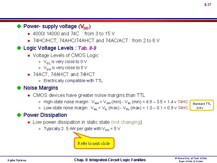
8 -37 u Power- supply voltage (VDD) l 4000/ 14000 and 74 C : from 3 to 15 V l 74 HC/HCT, 74 AHC/74 AHCT and 74 AC/ACT : from 2 to 6 V u Logic Voltage Levels : Tab. 8 -9 l Voltage Levels of CMOS Logic » VOL is very close to 0 V » VOH is very close to 5 V l 74 ACT, 74 AHCT and 74 HCT » Electrically compatible with TTL u Noise Margins l CMOS devices have greater noise margins than TTL » High-state noise margin : VNH = VOH (min) - VIH (min) = 4. 9 – 3. 5 = 1. 4 v 74 HC » Low-state noise margin : VNL = VIL (max) - VOL (max) = 1. 0 – 0. 1 = 0. 9 v 74 HC Standard TTL 0. 4 v u Power Dissipation l Low power dissipation in static state (not changing) » Typically 2. 5 n. W per gate with VDD = 5 V Refer to next slide Digital Systems Chap. 8 Integrated-Circuit Logic Families © Korea Univ. of Tech. & Edu. Dept. of Info. & Comm.
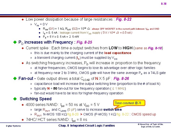
8 -38 l Low power dissipation because of large resistances : Fig. 8 -22 » VIN = 0 V n n n RON (Q 1) = 1 k , ROFF (Q 2) = 1010 : always OFF MOSFET in the current path between VDD and GND ID = 0. 5 n. A : leakage current from VDD supply ( 5 V / 1010 = 0. 5 n. A ) PD = 5 V x 0. 5 n. A = 2. 5 n. W u PD increases with Frequency : Fig. 8 -25 l Current spike : Each time a output switches from LOW to HIGH (same as Fig. 8 -18) » this is due mainly to the charging current of the load capacitance » a transient charging current (ID) must be supplied by VDD l As switching frequency increases, PD will increase in proportion to the frequency » at higher frequencies, CMOS begins to lose its advantage over other logic families » at frequency near 2 to 3 MHz, CMOS gate will have the same average PD as a 74 LS gate u Fan-out - Gate output drives a total CLOAD of N X 5 p. F : Fig. 8 -26 » capacitance load will increase the output switching time (proportion to the # of load N) » typically N = 50 fan-out for low frequency operation ( 1 MHz) » fan-out would have to be less for higher-frequency operation u Switching Speed l 4000 series NAND : tpd = 50 ns at VDD = 5 V Time-constant 증가 » large ROUT and CLOAD (5 p. F) serve to increase switch time » ROUT N-MOS 100 K fig. 8 -20 > CMOS (P-MOS) 1 K fig. 8 -22 : CMOS speed up l Digital Systems 74 HC/ HCT series NAND : tpd = 8 ns Chap. 8 Integrated-Circuit Logic Families © Korea Univ. of Tech. & Edu. Dept. of Info. & Comm.
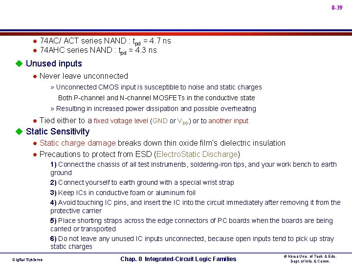
8 -39 74 AC/ ACT series NAND : tpd = 4. 7 ns l 74 AHC series NAND : tpd = 4. 3 ns l u Unused inputs l Never leave unconnected » Unconnected CMOS input is susceptible to noise and static charges Both P-channel and N-channel MOSFETs in the conductive state » Resulting in increased power dissipation and possible overheating l Tied either to a fixed voltage level (GND or VDD) or to another input u Static Sensitivity l Static charge damage breaks down thin oxide film’s dielectric insulation l Precautions to protect from ESD (Electro. Static Discharge) 1) Connect the chassis of all test instruments, soldering-iron tips, and your work bench to earth ground 2) Connect yourself to earth ground with a special wrist strap 3) Keep ICs in conductive foam or aluminum foil 4) Avoid touching IC pins, and insert the IC into the circuit immediately after removing it from the protective carrier 5) Place shorting straps across the edge connectors of PC boards when the boards are being carried or transported 6) Do not leave any unused IC inputs unconnected, because open inputs tend to pick up stray static charges Digital Systems Chap. 8 Integrated-Circuit Logic Families © Korea Univ. of Tech. & Edu. Dept. of Info. & Comm.
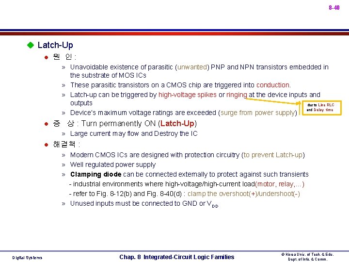
8 -40 u Latch-Up l 원 인: » Unavoidable existence of parasitic (unwanted) PNP and NPN transistors embedded in the substrate of MOS ICs » These parasitic transistors on a CMOS chip are triggered into conduction. » Latch-up can be triggered by high-voltage spikes or ringing at the device inputs and outputs • due to Line RLC and Delay time » Device’s maximum voltage ratings are exceeded (surge from power supply) l 증 상 : Turn permanently ON (Latch-Up) » Large current may flow and Destroy the IC l 해결책 : » Modern CMOS ICs are designed with protection circuitry (to prevent Latch-up) » Well regulated power supply » Clamping diode can be connected externally to protect against such transients - industrial environments where high-voltage/high-current load(motor, relay, …) - refer to Fig. 8 -12(b) and Fig. 8 -40(d) : clamp the overshoot(+)/undershoot(-) » Unused inputs must be connected to GND or VDD Digital Systems Chap. 8 Integrated-Circuit Logic Families © Korea Univ. of Tech. & Edu. Dept. of Info. & Comm.
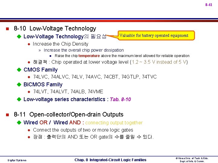
8 -41 n 8 -10 Low-Voltage Technology u Low-Voltage Technology의 필요성 l Increase the Chip Density Valuable for battery operated equipment » Increase the overall chip power dissipation n l Raise the chip temperature above the maximum level allowed for reliable operation 해결책 : Chip operated at lower voltage level (1. 2 ~ 3. 5 V instead of 5 V) u CMOS Family l 74 LVC, 74 ALVC, 74 LV, 74 AVC, 74 CBT, 74 GTLP, 74 TVC u Bi. CMOS Family l 74 LVT, 74 ALB, 74 VME u Low-voltage series characteristics : Tab. 8 -10 n 8 -11 Open-collector/Open-drain Outputs u Wired OR / Wired AND : connecting output together l Connect the outputs of two or more logic gates l 장점 : 출력단의 AND 또는 OR gate의 수를 줄일 수 있다. Digital Systems Chap. 8 Integrated-Circuit Logic Families © Korea Univ. of Tech. & Edu. Dept. of Info. & Comm.
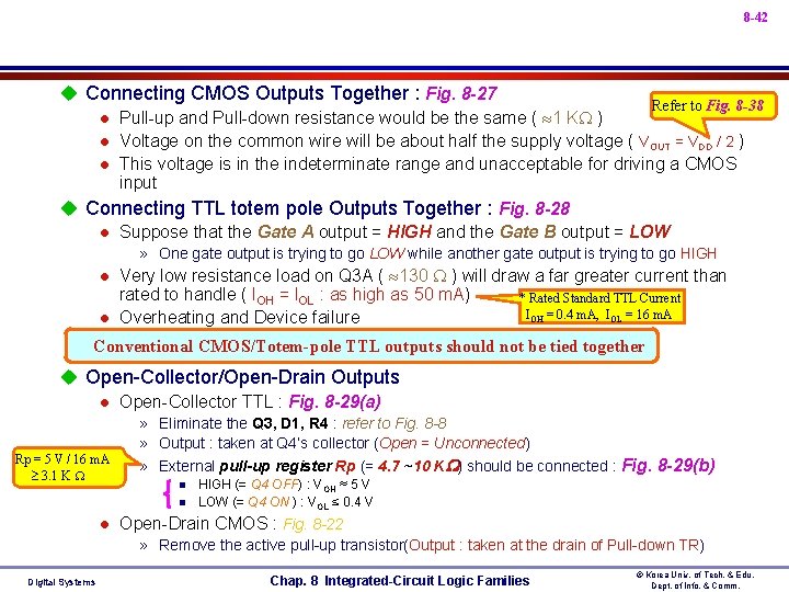
8 -42 u Connecting CMOS Outputs Together : Fig. 8 -27 Refer to Fig. 8 -38 l Pull-up and Pull-down resistance would be the same ( 1 K ) l Voltage on the common wire will be about half the supply voltage ( VOUT = VDD / 2 ) l This voltage is in the indeterminate range and unacceptable for driving a CMOS input u Connecting TTL totem pole Outputs Together : Fig. 8 -28 l Suppose that the Gate A output = HIGH and the Gate B output = LOW » One gate output is trying to go LOW while another gate output is trying to go HIGH l l Very low resistance load on Q 3 A ( 130 ) will draw a far greater current than rated to handle ( IOH = IOL : as high as 50 m. A) * Rated Standard TTL Current IOH = 0. 4 m. A, IOL = 16 m. A Overheating and Device failure Conventional CMOS/Totem-pole TTL outputs should not be tied together u Open-Collector/Open-Drain Outputs l Open-Collector TTL : Fig. 8 -29(a) Rp = 5 V / 16 m. A 3. 1 K » Eliminate the Q 3, D 1, R 4 : refer to Fig. 8 -8 » Output : taken at Q 4’s collector (Open = Unconnected) » External pull-up register Rp (= 4. 7 ~10 K ) should be connected : Fig. 8 -29(b) n n l HIGH (= Q 4 OFF) : VOH ≈ 5 V LOW (= Q 4 ON ) : VOL ≤ 0. 4 V Open-Drain CMOS : Fig. 8 -22 » Remove the active pull-up transistor(Output : taken at the drain of Pull-down TR) Digital Systems Chap. 8 Integrated-Circuit Logic Families © Korea Univ. of Tech. & Edu. Dept. of Info. & Comm.
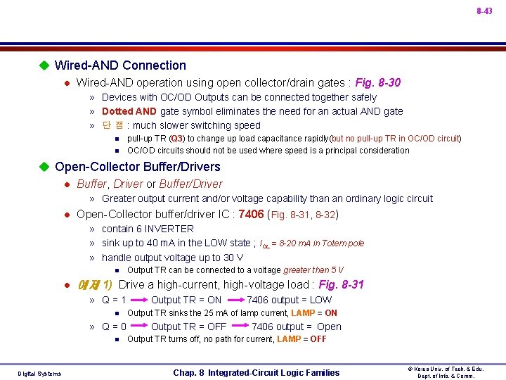
8 -43 u Wired-AND Connection l Wired-AND operation using open collector/drain gates : Fig. 8 -30 » Devices with OC/OD Outputs can be connected together safely » Dotted AND gate symbol eliminates the need for an actual AND gate » 단 점 : much slower switching speed n n pull-up TR (Q 3) to change up load capacitance rapidly(but no pull-up TR in OC/OD circuit) OC/OD circuits should not be used where speed is a principal consideration u Open-Collector Buffer/Drivers l Buffer, Driver or Buffer/Driver » Greater output current and/or voltage capability than an ordinary logic circuit l Open-Collector buffer/driver IC : 7406 (Fig. 8 -31, 8 -32) » contain 6 INVERTER » sink up to 40 m. A in the LOW state ; IOL = 8 -20 m. A in Totem pole » handle output voltage up to 30 V n l 예제 1) Drive a high-current, high-voltage load : Fig. 8 -31 » Q=1 n » Q=0 n Digital Systems Output TR can be connected to a voltage greater than 5 V Output TR = ON 7406 output = LOW Output TR sinks the 25 m. A of lamp current, LAMP = ON Output TR = OFF 7406 output = Open Output TR turns off, no path for current, LAMP = OFF Chap. 8 Integrated-Circuit Logic Families © Korea Univ. of Tech. & Edu. Dept. of Info. & Comm.
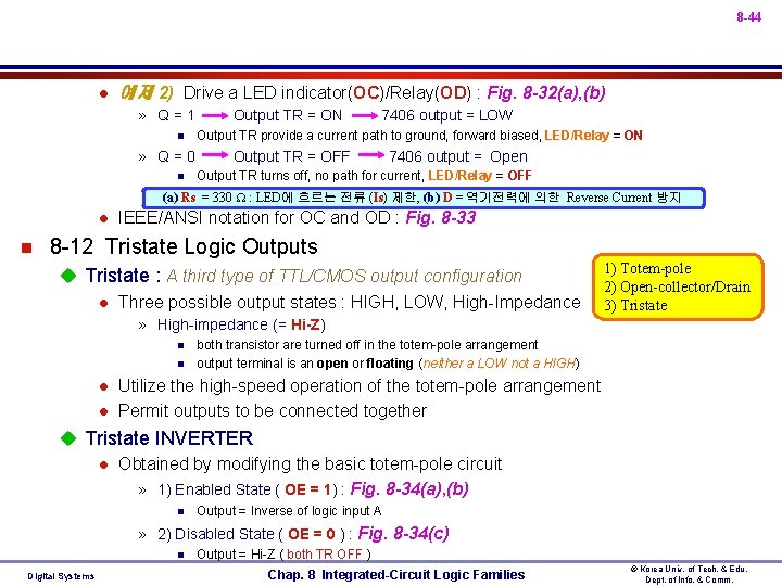
8 -44 l 예제 2) Drive a LED indicator(OC)/Relay(OD) : Fig. 8 -32(a), (b) » Q=1 n » Q=0 n Output TR = ON 7406 output = LOW Output TR provide a current path to ground, forward biased, LED/Relay = ON Output TR = OFF 7406 output = Open Output TR turns off, no path for current, LED/Relay = OFF (a) Rs = 330 : LED에 흐르는 전류 (Is) 제한, (b) D = 역기전력에 의한 Reverse Current 방지 l n IEEE/ANSI notation for OC and OD : Fig. 8 -33 8 -12 Tristate Logic Outputs u Tristate : A third type of TTL/CMOS output configuration l Three possible output states : HIGH, LOW, High-Impedance 1) Totem-pole 2) Open-collector/Drain 3) Tristate » High-impedance (= Hi-Z) n n l l both transistor are turned off in the totem-pole arrangement output terminal is an open or floating (neither a LOW not a HIGH) Utilize the high-speed operation of the totem-pole arrangement Permit outputs to be connected together u Tristate INVERTER l Obtained by modifying the basic totem-pole circuit » 1) Enabled State ( OE = 1) : Fig. 8 -34(a), (b) n Output = Inverse of logic input A » 2) Disabled State ( OE = 0 ) : Fig. 8 -34(c) n Digital Systems Output = Hi-Z ( both TR OFF ) Chap. 8 Integrated-Circuit Logic Families © Korea Univ. of Tech. & Edu. Dept. of Info. & Comm.
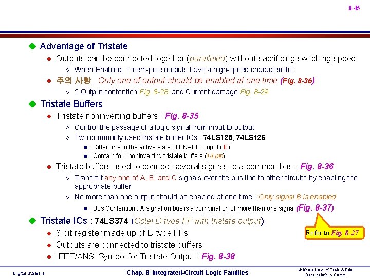
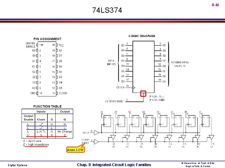
8 -45 u Advantage of Tristate l Outputs can be connected together (paralleled) without sacrificing switching speed. » When Enabled, Totem-pole outputs have a high-speed characteristic l 주의 사항 : Only one of output should be enabled at one time (Fig. 8 -36) » 2 Output contention Fig. 8 -28 and Current damage Fig. 8 -29 u Tristate Buffers l Tristate noninverting buffers : Fig. 8 -35 » Control the passage of a logic signal from input to output » Two commonly used tristate buffer ICs : 74 LS 125, 74 LS 126 n n l Differ only in the active state of ENABLE input ( E) Contain four noninverting tristate buffers (14 pin) Tristate buffers used to connect several signals to a common bus : Fig. 8 -36 » Transmit any one of A, B, and C signals over the bus line to other circuits by enabling the appropriate buffer » No more than one output should be enabled at one time : Only signal B is enabled n Bus Contention : A signal on bus is a combination of more than one signal (Fig. u Tristate ICs : 74 LS 374 (Octal D-type FF with tristate output) l 8 -bit register made up of D-type FFs l Outputs are connected to tristate buffers l IEEE/ANSI Symbol for Tristate Output : Fig. 8 -38 Digital Systems Chap. 8 Integrated-Circuit Logic Families 8 -37) Refer to Fig. 8 -27 © Korea Univ. of Tech. & Edu. Dept. of Info. & Comm.
• 74 LS 374 8 -46 Active LOW Digital Systems Chap. 8 Integrated-Circuit Logic Families © Korea Univ. of Tech. & Edu. Dept. of Info. & Comm.
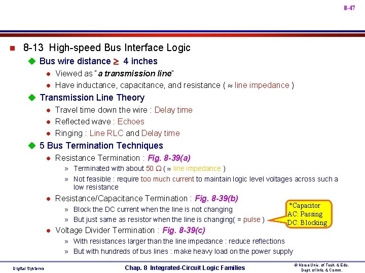
8 -47 n 8 -13 High-speed Bus Interface Logic u Bus wire distance 4 inches l Viewed as “a transmission line” l Have inductance, capacitance, and resistance ( line impedance ) u Transmission Line Theory l Travel time down the wire : Delay time l Reflected wave : Echoes l Ringing : Line RLC and Delay time u 5 Bus Termination Techniques l Resistance Termination : Fig. 8 -39(a) » Terminated with about 50 ( line impedance ) » Not feasible : require too much current to maintain logic level voltages across such a low resistance l Resistance/Capacitance Termination : Fig. 8 -39(b) » Block the DC current when the line is not changing » But just same as resistor when the line is changing( = pulse ) l Voltage Divider Termination : Fig. 8 -39(c) *Capacitor AC: Passing DC: Blocking » With resistances larger than the line impedance : reduce reflections » But with hundreds of bus lines : make heavy load on the power supply Digital Systems Chap. 8 Integrated-Circuit Logic Families © Korea Univ. of Tech. & Edu. Dept. of Info. & Comm.
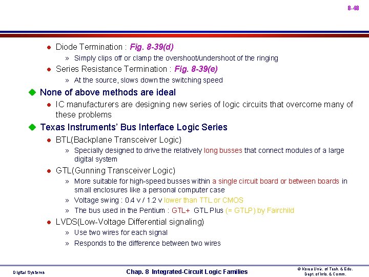
8 -48 l Diode Termination : Fig. 8 -39(d) » Simply clips off or clamp the overshoot/undershoot of the ringing l Series Resistance Termination : Fig. 8 -39(e) » At the source, slows down the switching speed u None of above methods are ideal l IC manufacturers are designing new series of logic circuits that overcome many of these problems u Texas Instruments’ Bus Interface Logic Series l BTL(Backplane Transceiver Logic) » Specially designed to drive the relatively long busses that connect modules of a large digital system l GTL(Gunning Transceiver Logic) » More suitable for high-speed busses within a single circuit board or between boards in small enclosures like a personal computer case » Voltage swing : 0. 4 v / 1. 2 v lower than TTL or CMOS » The bus used in the Pentium : GTL+ GTL Plus (= GTLP) by Fairchild l LVDS(Low-Voltage Differential signaling) » Use two wires for each signal » Responds to the difference between two wires Digital Systems Chap. 8 Integrated-Circuit Logic Families © Korea Univ. of Tech. & Edu. Dept. of Info. & Comm.
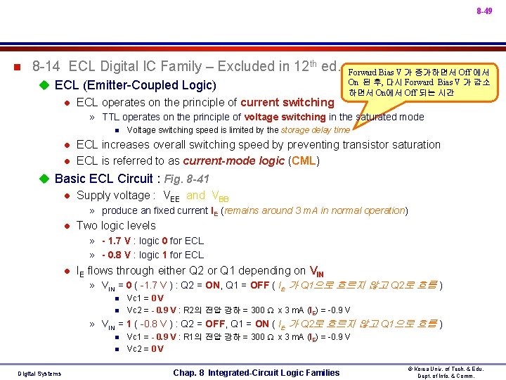
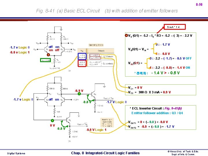
8 -49 n 8 -14 ECL Digital IC Family – Excluded in 12 th ed. u ECL (Emitter-Coupled Logic) l ECL operates on the principle of current switching Forward Bias V 가 증가하면서 Off 에서 On 된 후, 다시 Forward Bias V 가 감소 하면서 On에서 Off 되는 시간 » TTL operates on the principle of voltage switching in the saturated mode n l l Voltage switching speed is limited by the storage delay time ECL increases overall switching speed by preventing transistor saturation ECL is referred to as current-mode logic (CML) u Basic ECL Circuit : Fig. 8 -41 l Supply voltage : VEE and VBB » produce an fixed current IE (remains around 3 m. A in normal operation) l Two logic levels » - 1. 7 V : logic 0 for ECL » - 0. 8 V : logic 1 for ECL l IE flows through either Q 2 or Q 1 depending on VIN » VIN = 0 ( -1. 7 V ) : Q 2 = ON, Q 1 = OFF ( IE 가 Q 1으로 흐르지 않고 Q 2로 흐름 ) n n Vc 1 = 0 V Vc 2 = - 0. 9 V : R 2의 전압 강하 = 300 x 3 m. A (IE) = -0. 9 V » VIN = 1 ( -0. 8 V ) : Q 2 = OFF, Q 1 = ON ( IE 가 Q 2로 흐르지 않고 Q 1으로 흐름 ) n n Digital Systems Vc 1 = - 0. 9 V : R 1의 전압 강하 = 300 x 3 m. A (IE) = -0. 9 V Vc 2 = 0 V Chap. 8 Integrated-Circuit Logic Families © Korea Univ. of Tech. & Edu. Dept. of Info. & Comm.
8 -50 • Fig. 8 -41 (a) Basic ECL Circuit (b) with addition of emitter followers • 3 m. A * 1 K • -1. 7 v Logic 0 • -0. 8 v Logic 1 • VE (Q 1) = -5. 2 – IE * R 3 = -5. 2 – (- 3) = - 2. 2 V • • 0 : - 1. 7 V • VB(Q 1) = VIN = • 1 : - 0. 8 V • 0 : -2. 2 – (- 1. 7) = - 0. 5 V OFF • VBE(Q 1) = • 1 : -2. 2 – (- 0. 8) = - 1. 4 V ON • off • on • off • • off • on - 1. 4 V > - 0. 5 V • VC 1 = 0 V • VC 2 = 300 Ω X 3 m. A = 0. 9 V • -0. 9 V • -1. 7 v Logic 0 * 전위차 : • -0. 8 V • -1. 7 V Logic 0 • * ECL Inverter Circuit : Fig. 8 -41(b) • Emitter follower addition : Q 3 / Q 4 • 0 V Digital Systems • -0. 8 V Logic 1 • VOUT 1 = 0 + (– 0. 8 ) = -0. 8 V • VOUT 2 = -0. 9 + (– 0. 8 ) = - 1. 7 V Chap. 8 Integrated-Circuit Logic Families © Korea Univ. of Tech. & Edu. Dept. of Info. & Comm.
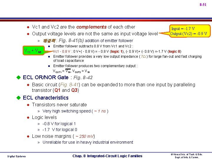
8 -51 l l Vc 1 and Vc 2 are the complements of each other Output voltage levels are not the same as input voltage level » 해결책 : Fig. 8 -41(b) addition of emitter follower n VC 1 + VBE n n Input = -1. 7 V Output (Vc 2) = -0. 9 V Emitter follower subtracts 0. 8 V from Vc 1 and Vc 2 : Vc 1 - 0. 8 V : 0 V+( - 0. 8 V) = - 0. 8 V (logic 1), (- 0. 9 V)+ (- 0. 8 V) =-1. 7 V (logic 0) Emitter follower provides a very low output impedance ( 7 ) for large fan-out and fast charging of load capacitance Emitter follower produces two complementary output : VOUT 1 = VIN, VOUT 2 = VIN u ECL OR/NOR Gate : Fig. 8 -42 l Basic circuit (Fig. 8 -41) can be expanded to more than one input by paralleling transistor (Q 1 and Q 3) u ECL characteristics l Transistors never saturate » Very high switching speed ( ~ 1 ns ) l Logic levels » -0. 8 V for logical 1 » -1. 7 V for logical 0 l Low noise margins ( ~ 250 m. V) » Unreliable for use in heavy industrial environment Digital Systems Chap. 8 Integrated-Circuit Logic Families © Korea Univ. of Tech. & Edu. Dept. of Info. & Comm.
8 -52 l Generates normal output and its complement output » Eliminate the need for INVERTER l l Fan- out around 25 25 m. W power dissipation » Higher than with other logic families l No noise spikes » Current switching u ECL comparison with other logic families : Tab. 8 -11 l High speed (short propagation delay) : high clock rate l High power dissipation l Low noise margin u Disadvantage of ECL l Not a wide range of general-purpose logic devices » only special purpose ICs : high-speed data transmission, high-speed memory, highspeed arithmetic units l l l Relatively low noise margins and high power dissipation 2 Negative power supply voltage ( VEE and VBB ) Difficult to use ECL devices with TTL or CMOS ICs » Logic levels are not compatible with other logic families Digital Systems Chap. 8 Integrated-Circuit Logic Families © Korea Univ. of Tech. & Edu. Dept. of Info. & Comm.
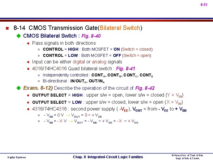
8 -53 n 8 -14 CMOS Transmission Gate(Bilateral Switch) u CMOS Bilateral Switch : Fig. 8 -40 l Pass signals in both directions » CONTROL = HIGH : Both MOSFET = ON (Switch = closed) » CONTROL = LOW : Both MOSFET = OFF (Switch = open) l l Input can be either digital or analog signals 4016/74 HC 4016 Quad bilateral switch : Fig. 8 -41 » Independently controlled : CONTA, CONTB, CONTC, CONTD » Bi-directional : IN/OUTA, OUT/INA u Exam. 8 -12) Describe the operation of the circuit of Fig. 8 -42 l OUTPUT SELECT = HIGH : upper s/w = open, lower s/w = closed (Y = VIN) l OUTPUT SELECT = LOW : upper s/w = closed, lower s/w = open (X = VIN) l 4316/74 HC 4316 : second power supply ( -VEE), VOUT = from - VEE to + VDD » - VEE = 0 V → VOUT = 0 ~ + VDD » - VEE = - X V → VOUT = - VEE ~ + VDD = - X ~ + VDD Digital Systems Chap. 8 Integrated-Circuit Logic Families © Korea Univ. of Tech. & Edu. Dept. of Info. & Comm.
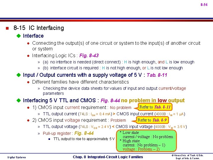
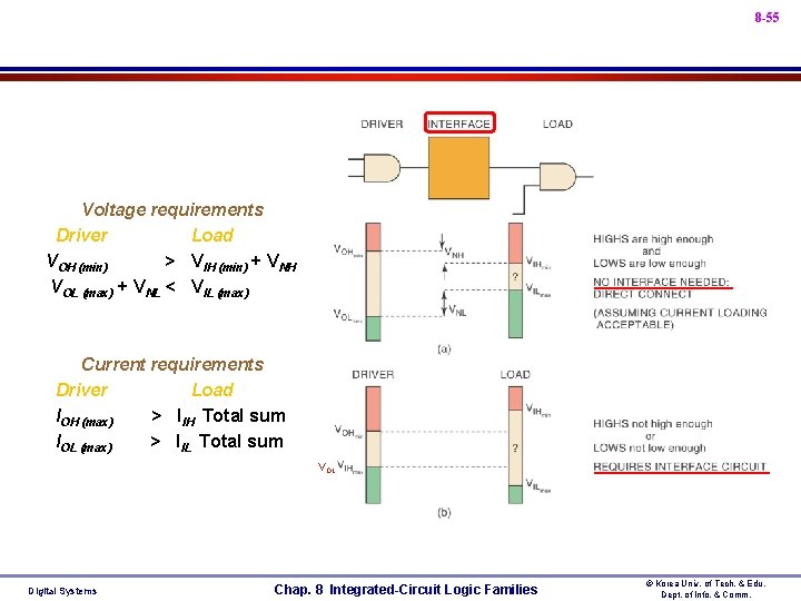
8 -54 n 8 -15 IC Interfacing u Interface l Connecting the output(s) of one circuit or system to the input(s) of another circuit or system l Interfacing Logic ICs : Fig. 8 -43 » (a) no interface is needed (direct connect) : H is high enough, and L is low enough » (b) interface circuit is required : H is not high enough, or L is not low enough u Input / Output currents with a supply voltage of 5 V : Tab. 8 -11 l Different families have different characteristics » Checking the device data sheets for values of input and output current/voltage parameters u Interfacing 5 V TTL and CMOS : Fig. 8 -44 no problem in low output Refer to Tab. 8 -11 l 1) CMOS input current requirement : No problem » TTL output current (74 LS : IOH = 0. 4 m. A) > CMOS input current (4000 B : IIH = 1 A) Refer to Tab. 8 -9 l 2) CMOS input voltage requirement : Problem » TTL output voltage (74 LS : VOH = 2. 4 V) < CMOS input voltage (4000 B : VIH = 3. 5 V) * Low state » Pull-up register : Fig. 8 -44 current / voltage : No problem n TTL output to rise to approximately 5 V * High state current : No problem – 1) voltage : Problem – 2) Digital Systems Chap. 8 Integrated-Circuit Logic Families © Korea Univ. of Tech. & Edu. Dept. of Info. & Comm.
8 -55 • Voltage requirements • Driver Load • VOH (min) > VIH (min) + VNH • VOL (max) + VNL < VIL (max) • Current requirements • Driver Load • IOH (max) > IIH Total sum • IOL (max) > IIL Total sum • VOL Digital Systems Chap. 8 Integrated-Circuit Logic Families © Korea Univ. of Tech. & Edu. Dept. of Info. & Comm.
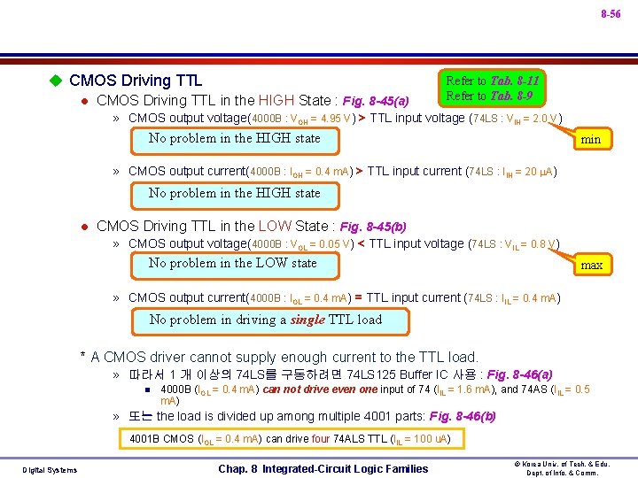
8 -56 u CMOS Driving TTL l CMOS Driving TTL in the HIGH State : Fig. 8 -45(a) Refer to Tab. 8 -11 Refer to Tab. 8 -9 » CMOS output voltage(4000 B : VOH = 4. 95 V) > TTL input voltage (74 LS : VIH = 2. 0 V) No problem in the HIGH state min » CMOS output current(4000 B : IOH = 0. 4 m. A) > TTL input current (74 LS : IIH = 20 A) No problem in the HIGH state l CMOS Driving TTL in the LOW State : Fig. 8 -45(b) » CMOS output voltage(4000 B : VOL = 0. 05 V) < TTL input voltage (74 LS : VIL = 0. 8 V) No problem in the LOW state max » CMOS output current(4000 B : IOL = 0. 4 m. A) = TTL input current (74 LS : IIL = 0. 4 m. A) No problem in driving a single TTL load * A CMOS driver cannot supply enough current to the TTL load. » 따라서 1 개 이상의 74 LS를 구동하려면 74 LS 125 Buffer IC 사용 : Fig. 8 -46(a) n 4000 B (IOL = 0. 4 m. A) can not drive even one input of 74 (IIL = 1. 6 m. A), and 74 AS (IIL = 0. 5 m. A) » 또는 the load is divided up among multiple 4001 parts: Fig. 8 -46(b) 4001 B CMOS (IOL = 0. 4 m. A) can drive four 74 ALS TTL (IIL = 100 u. A) Digital Systems Chap. 8 Integrated-Circuit Logic Families © Korea Univ. of Tech. & Edu. Dept. of Info. & Comm.
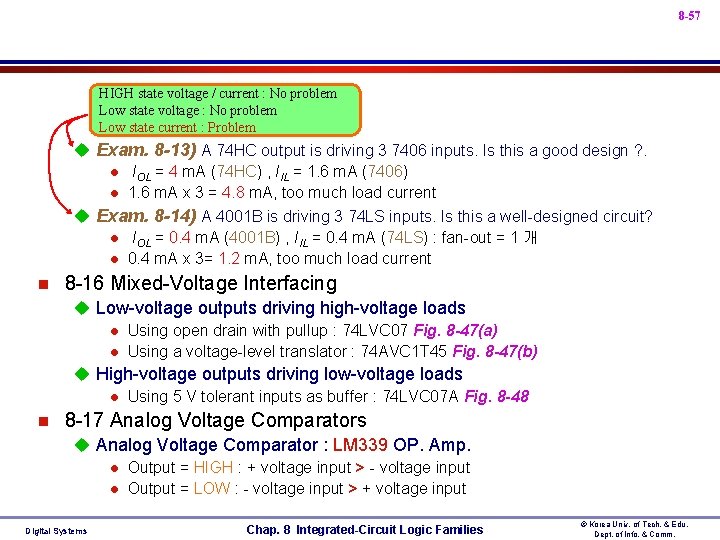
8 -57 HIGH state voltage / current : No problem Low state voltage : No problem Low state current : Problem u Exam. 8 -13) A 74 HC output is driving 3 7406 inputs. Is this a good design ? . l IOL = 4 m. A (74 HC) , IIL = 1. 6 m. A (7406) l 1. 6 m. A x 3 = 4. 8 m. A, too much load current u Exam. 8 -14) A 4001 B is driving 3 74 LS inputs. Is this a well-designed circuit? l IOL = 0. 4 m. A (4001 B) , IIL = 0. 4 m. A (74 LS) : fan-out = 1 개 l 0. 4 m. A x 3= 1. 2 m. A, too much load current n 8 -16 Mixed-Voltage Interfacing u Low-voltage outputs driving high-voltage loads l Using open drain with pullup : 74 LVC 07 Fig. 8 -47(a) l Using a voltage-level translator : 74 AVC 1 T 45 Fig. 8 -47(b) u High-voltage outputs driving low-voltage loads l Using 5 V tolerant inputs as buffer : 74 LVC 07 A Fig. 8 -48 n 8 -17 Analog Voltage Comparators u Analog Voltage Comparator : LM 339 OP. Amp. l Output = HIGH : + voltage input > - voltage input l Output = LOW : - voltage input > + voltage input Digital Systems Chap. 8 Integrated-Circuit Logic Families © Korea Univ. of Tech. & Edu. Dept. of Info. & Comm.
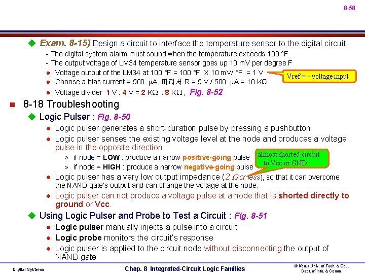
8 -58 u Exam. 8 -15) Design a circuit to interface the temperature sensor to the digital circuit. - The digital system alarm must sound when the temperature exceeds 100 °F - The output voltage of LM 34 temperature sensor goes up 10 m. V per degree F l Voltage output of the LM 34 at 100 °F = 100 °F X 10 m. V/ °F = 1 V Vref = - voltage input l Choose a bias current = 500 A, 따라서 R = 5 V / 500 A = 10 K l Voltage divider 1 V : 4 V = 2 K : 8 K , Fig. 8 -52 n 8 -18 Troubleshooting u Logic Pulser : Fig. 8 -50 l Logic pulser generates a short-duration pulse by pressing a pushbutton l Logic pulser senses the existing voltage level at the node and produces a voltage pulse in the opposite direction » if node = LOW : produce a narrow positive-going pulse almost shorted circuit to Vcc or GND » if node = HIGH : produce a narrow negative-going pulse l Logic pulser has a very low output impedance (2 or less), so that it can overcome the NAND gate’s output and can change the voltage at the node. Logic pulser can not produce a voltage pulse at a node that is shorted directly to ground or Vcc. u Using Logic Pulser and Probe to Test a Circuit : Fig. 8 -51 l Logic pulser manually injects a pulse into a circuit l Logic probe monitors the circuit’s response l Logic pulser is applied to the circuit node without disconnecting the output of NAND gate l Digital Systems Chap. 8 Integrated-Circuit Logic Families © Korea Univ. of Tech. & Edu. Dept. of Info. & Comm.
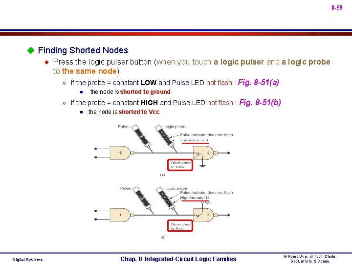
8 -59 u Finding Shorted Nodes l Press the logic pulser button (when you touch a logic pulser and a logic probe to the same node) » if the probe = constant LOW and Pulse LED not flash : Fig. 8 -51(a) n the node is shorted to ground » if the probe = constant HIGH and Pulse LED not flash : Fig. 8 -51(b) n Digital Systems the node is shorted to Vcc Chap. 8 Integrated-Circuit Logic Families © Korea Univ. of Tech. & Edu. Dept. of Info. & Comm.
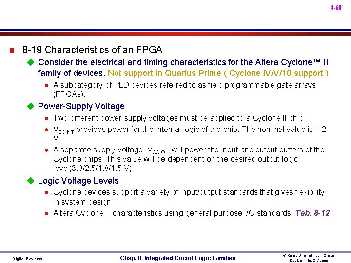
8 -60 n 8 -19 Characteristics of an FPGA u Consider the electrical and timing characteristics for the Altera Cyclone™ II family of devices. Not support in Quartus Prime ( Cyclone IV/V/10 support ) l A subcategory of PLD devices referred to as field programmable gate arrays (FPGAs). u Power-Supply Voltage l Two different power-supply voltages must be applied to a Cyclone II chip. l VCCINT provides power for the internal logic of the chip. The nominal value is 1. 2 V l A separate supply voltage, VCCIO , will power the input and output buffers of the Cyclone chips. This value will be dependent on the desired output logic level(3. 3/2. 5/1. 8/1. 5 V) u Logic Voltage Levels l Cyclone devices support a variety of input/output standards that gives flexibility in system design l Altera Cyclone II characteristics using general-purpose I/O standards: Tab. 8 -12 Digital Systems Chap. 8 Integrated-Circuit Logic Families © Korea Univ. of Tech. & Edu. Dept. of Info. & Comm.
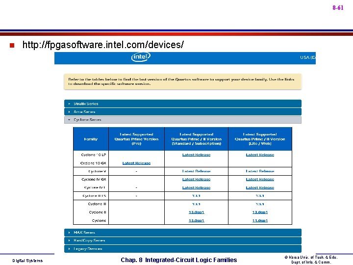
8 -61 n http: //fpgasoftware. intel. com/devices/ Digital Systems Chap. 8 Integrated-Circuit Logic Families © Korea Univ. of Tech. & Edu. Dept. of Info. & Comm.
8 -62 u Power Dissipation l The Cyclone II devices use CMOS, so power consumption will be low—power will be dependent on voltage level, frequencies & I/O signal loads. l The Quartus II software has two tools to estimate the amount the power usage for an application. » The Power. Play Early Power Estimator is typically used during the early stages of design. » The Power. Play Power Analyzer is often used with sample test vectors, for more accurate estimate. u Maximum Input Voltage and Output Current Ratings l The Max. DC Input Voltage : 4. 6 V l Each output pin can sink up to 40 m. A / source up to 25 m. A u Switching Speed l The speed of an application will be dependent upon the application and how it is implemented in the programmable device : Tab. 8 -13 l Cyclone II chips are available in three different speed grades ( – 6 , – 7, and – 8 ) Digital Systems Chap. 8 Integrated-Circuit Logic Families © Korea Univ. of Tech. & Edu. Dept. of Info. & Comm.