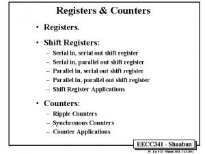
7 1 Chap 7 Counters and Registers n

- Slides: 53
7 -1 Chap. 7 Counters and Registers n Chapter Outcomes (Objectives) u Describe the operation and characteristics of synchronous and asynchronous u u u Digital Systems counters. Construct counters with MOD numbers less than 2 N. Construct both up and down counters. Connect multistage counters. Analyze and evaluate various types of counters. Design arbitrary-sequence synchronous counters. Describe several schemes used to decode different types of counters. Describe counter circuits using different levels of abstraction in HDL. Construct shift register counters. Explain the operation of various types of IC registers. Describe shift registers and shift register counters using HDL. Apply troubleshooting techniques used for combinational logic systems to troubleshoot sequential logic systems. Chap. 7 Counters and Registers © Korea Univ. of Tech. & Edu. Dept. of Info. & Comm.
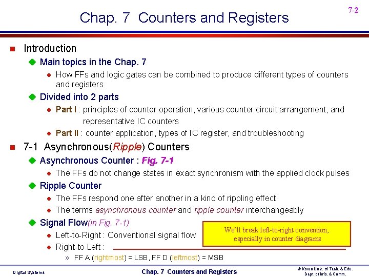
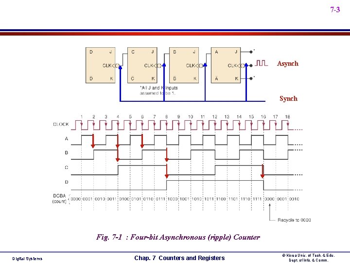
7 -2 Chap. 7 Counters and Registers n Introduction u Main topics in the Chap. 7 l How FFs and logic gates can be combined to produce different types of counters and registers u Divided into 2 parts l Part I : principles of counter operation, various counter circuit arrangement, and representative IC counters l Part II : counter application, types of IC register, and troubleshooting n 7 -1 Asynchronous(Ripple) Counters u Asynchronous Counter : Fig. 7 -1 l The FFs do not change states in exact synchronism with the applied clock pulses u Ripple Counter l The FFs respond one after another in a kind of rippling effect l The terms asynchronous counter and ripple counter interchangeably u Signal Flow(in Fig. 7 -1) l Left-to-Right : Conventional signal flow l Right-to Left : We’ll break left-to-right convention, especially in counter diagrams » FF A (rightmost) = LSB, FF D (leftmost) = MSB Digital Systems Chap. 7 Counters and Registers © Korea Univ. of Tech. & Edu. Dept. of Info. & Comm.
7 -3 Asynch Synch Fig. 7 -1 : Four-bit Asynchronous (ripple) Counter Digital Systems Chap. 7 Counters and Registers © Korea Univ. of Tech. & Edu. Dept. of Info. & Comm.
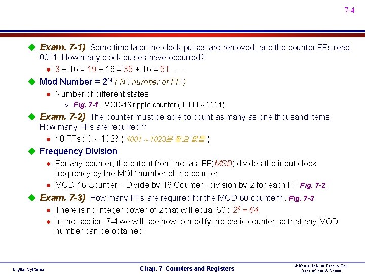
7 -4 u Exam. 7 -1) Some time later the clock pulses are removed, and the counter FFs read 0011. How many clock pulses have occurred? l 3 + 16 = 19 + 16 = 35 + 16 = 51 …. . u Mod Number = 2 N ( N : number of FF ) l Number of different states » Fig. 7 -1 : MOD-16 ripple counter ( 0000 1111) u Exam. 7 -2) The counter must be able to count as many as one thousand items. How many FFs are required ? l 10 FFs : 0 1023 ( 1001 1023은 필요 없음 ) u Frequency Division l For any counter, the output from the last FF(MSB) divides the input clock frequency by the MOD number of the counter l MOD-16 Counter = Divide-by-16 Counter : division by 2 for each FF Fig. 7 -2 u Exam. 7 -3) How many FFs are required for the MOD-60 counter? : Fig. 7 -3 l There is no integer power of 2 that will equal 60 : 26 = 64 l In the section 7 -4 we will see how to modify the basic counter so that any MOD number can be obtained. Digital Systems Chap. 7 Counters and Registers © Korea Univ. of Tech. & Edu. Dept. of Info. & Comm.
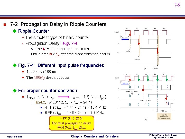
7 -5 n 7 -2 Propagation Delay in Ripple Counters u Ripple Counter + The simplest type of binary counter - Propagation Delay : Fig. 7 -4 » The Nth FF cannot change states until a time N x tpd after the clock transition occurs. u Fig. 7 -4 : Different input pulse frequencies l 1000 ns vs 100 ns l The 100(4) does not occur u For proper counter operation l Tclock N x tpd fmax = 1 /( N x tpd ) » Exam) 74 LS 112, tpd = t. PHL = 24 ns n 4 FFs : fmax = 1 / 4 x 24 ns = 10. 4 MHz n 6 FFs : fmax = 1 / 6 x 24 ns = 6. 9 MHz 0 1 0 0 0 1 1 0 0 01 * FF 개수 증가 The total propagation delay 증가하고 fmax 감소 Digital Systems Chap. 7 Counters and Registers © Korea Univ. of Tech. & Edu. Dept. of Info. & Comm.
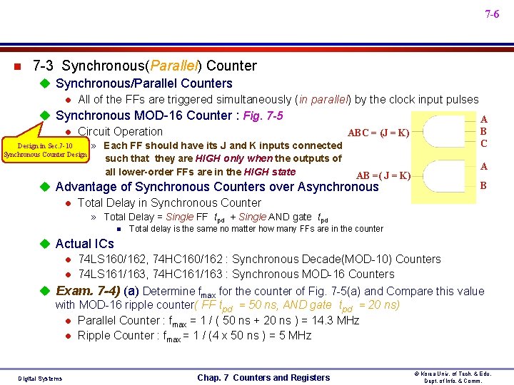
7 -6 n 7 -3 Synchronous(Parallel) Counter u Synchronous/Parallel Counters l All of the FFs are triggered simultaneously (in parallel) by the clock input pulses u Synchronous MOD-16 Counter : Fig. 7 -5 A B l Circuit Operation ABC = (J = K) Design in Sec. 7 -10 Synchronous Counter Design » Each FF should have its J and K inputs connected such that they are HIGH only when the outputs of all lower-order FFs are in the HIGH state C AB =( J = K) u Advantage of Synchronous Counters over Asynchronous l Total Delay in Synchronous Counter A B » Total Delay = Single FF tpd + Single AND gate tpd n Total delay is the same no matter how many FFs are in the counter u Actual ICs l 74 LS 160/162, 74 HC 160/162 : Synchronous Decade(MOD-10) Counters l 74 LS 161/163, 74 HC 161/163 : Synchronous MOD-16 Counters u Exam. 7 -4) (a) Determine fmax for the counter of Fig. 7 -5(a) and Compare this value with MOD-16 ripple counter( FF tpd = 50 ns, AND gate tpd = 20 ns) l Parallel Counter : fmax = 1 / ( 50 ns + 20 ns ) = 14. 3 MHz l Ripple Counter : fmax = 1 / (4 x 50 ns ) = 5 MHz Digital Systems Chap. 7 Counters and Registers © Korea Univ. of Tech. & Edu. Dept. of Info. & Comm.
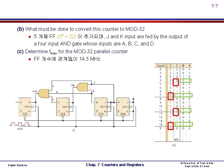
7 -7 (b) What must be done to convert this counter to MOD-32 l 5 개째 FF (25 = 32) 이 추가되며, J and K input are fed by the output of a four input AND gate whose inputs are A, B, C, and D (c) Determine fmax for the MOD-32 parallel counter l Digital Systems FF 개수에 관계없이 14. 3 MHz Chap. 7 Counters and Registers © Korea Univ. of Tech. & Edu. Dept. of Info. & Comm.
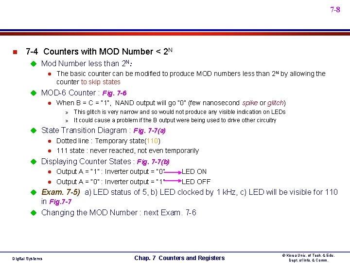
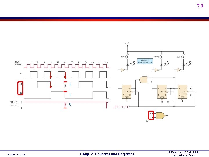
7 -8 n 7 -4 Counters with MOD Number < 2 N u Mod Number less than 2 N: l The basic counter can be modified to produce MOD numbers less than 2 N by allowing the counter to skip states u MOD-6 Counter : Fig. 7 -6 l When B = C = “ 1”, NAND output will go “ 0” (few nanosecond spike or glitch) » This glitch is very narrow and so would not produce any visible indication on LEDs » It could cause a problem if the B output were being used to drive other circuitry u State Transition Diagram : Fig. 7 -7(a) l l Dotted line : Temporary state(110) 111 state : never reached, not even temporarily u Displaying Counter States : Fig. 7 -7(b) l l Output A = “ 1” : Inverter output = “ 0” Output A = “ 0” : Inverter output = “ 1” LED ON LED OFF u Exam. 7 -5) a) LED status of 5, b) LED clocked by 1 k. Hz, c) LED will be visible for 110 in Fig. 7 -7 u Changing the MOD Number : next Exam. 7 -6 Digital Systems Chap. 7 Counters and Registers © Korea Univ. of Tech. & Edu. Dept. of Info. & Comm.
7 -9 1 1 0 Digital Systems Chap. 7 Counters and Registers © Korea Univ. of Tech. & Edu. Dept. of Info. & Comm.
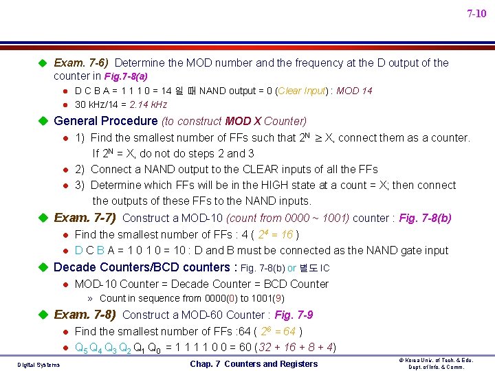
7 -10 u Exam. 7 -6) Determine the MOD number and the frequency at the D output of the counter in Fig. 7 -8(a) l l D C B A = 1 1 1 0 = 14 일 때 NAND output = 0 (Clear Input) : MOD 14 30 k. Hz/14 = 2. 14 k. Hz u General Procedure (to construct MOD X Counter) l 1) Find the smallest number of FFs such that 2 N X, connect them as a counter. If 2 N = X, do not do steps 2 and 3 l 2) Connect a NAND output to the CLEAR inputs of all the FFs l 3) Determine which FFs will be in the HIGH state at a count = X; then connect the outputs of these FFs to the NAND inputs. u Exam. 7 -7) Construct a MOD-10 (count from 0000 ~ 1001) counter : Fig. 7 -8(b) l Find the smallest number of FFs : 4 ( 24 = 16 ) l D C B A = 1 0 = 10 : D and B must be connected as the NAND gate input u Decade Counters/BCD counters : Fig. 7 -8(b) or 별도 IC l MOD-10 Counter = Decade Counter = BCD Counter » Count in sequence from 0000(0) to 1001(9) u Exam. 7 -8) Construct a MOD-60 Counter : Fig. 7 -9 l Find the smallest number of FFs : 64 ( 26 = 64 ) l Q 5 Q 4 Q 3 Q 2 Q 1 Q 0 = 1 1 0 0 = 60 (32 + 16 + 8 + 4) Digital Systems Chap. 7 Counters and Registers © Korea Univ. of Tech. & Edu. Dept. of Info. & Comm.
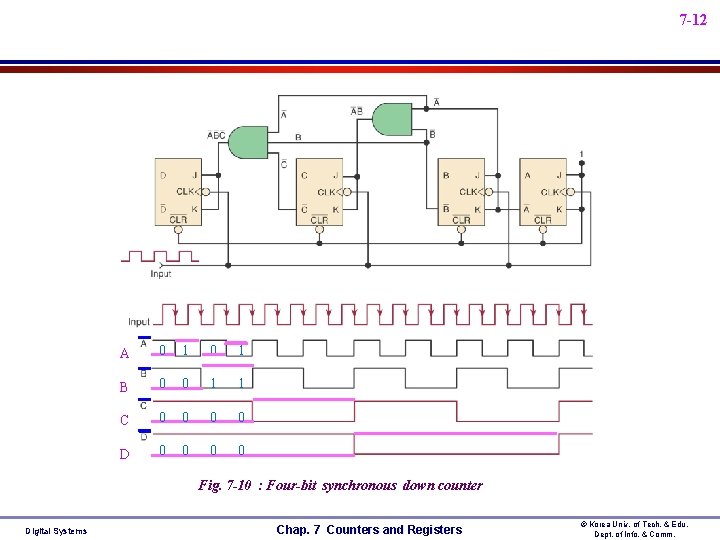
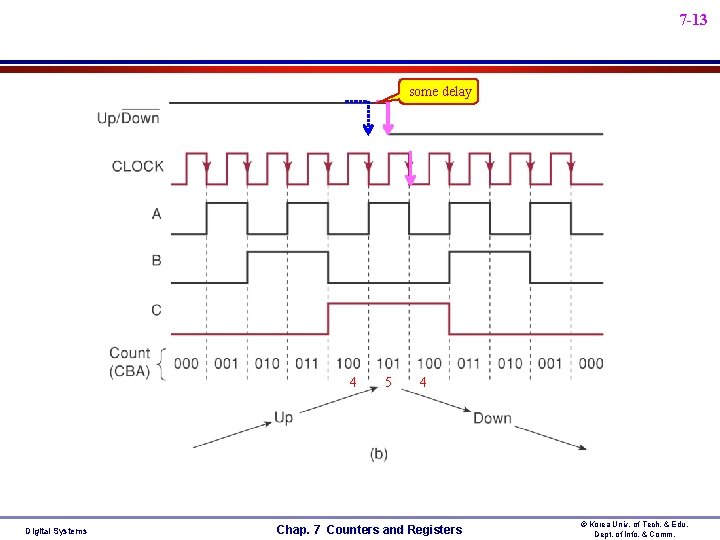
7 -11 n 7 -5 Synchronous Down and Up/Down Counters u MOD-16 Down Counter : Fig. 7 -10 l Constructed in a similar manner except that we use the inverted FF output to control the higher-order J, K inputs. u MOD-8 Parallel Up/Down Counter : Fig. 7 -11 l Up Count : Up/Down = 1, AND gates 1/2 = Enabled, AND gates 3/4 = Disabled l Down Count : Up/Down = 0, AND gates 1/2 = Disabled, AND gates 3/4 = Enabled u Exam. 7 -9) What problems might be caused if the Up/Down signal changes levels on the NGT of the clock ? l Possible Problems : Unpredictable results of FF » the J and K inputs change at about the same time that a NGT occurs at their CLK input. l Effects : Predictable results of FF (No problems) » the effects of the change in the control signal must propagate through two gates before reaching the J, K inputs (결국 다음 Clock에서 Up/Down 동작이 가능함) Digital Systems Chap. 7 Counters and Registers © Korea Univ. of Tech. & Edu. Dept. of Info. & Comm.
7 -12 A 0 1 B 0 0 1 1 C 0 0 D 0 0 Fig. 7 -10 : Four-bit synchronous down counter Digital Systems Chap. 7 Counters and Registers © Korea Univ. of Tech. & Edu. Dept. of Info. & Comm.
7 -13 some delay 4 Digital Systems 5 4 Chap. 7 Counters and Registers © Korea Univ. of Tech. & Edu. Dept. of Info. & Comm.
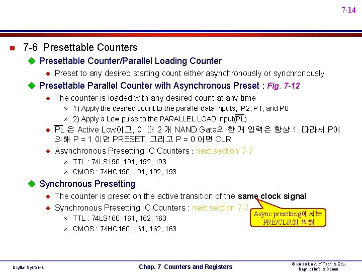
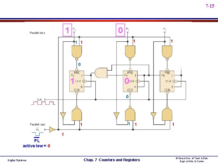
7 -14 n 7 -6 Presettable Counters u Presettable Counter/Parallel Loading Counter l Preset to any desired starting count either asynchronously or synchronously u Presettable Parallel Counter with Asynchronous Preset : Fig. 7 -12 l The counter is loaded with any desired count at any time » 1) Apply the desired count to the parallel data inputs, P 2, P 1, and P 0 » 2) Apply a Low pulse to the PARALLEL LOAD input(PL) l l PL 은 Active Low이고, 이 때 2 개 NAND Gate의 한 개 입력은 항상 1, 따라서 P에 의해 P = 1 이면 PRESET, 그리고 P = 0 이면 CLR Asynchronous Presetting IC Counters : next section 7 -7 » TTL : 74 LS 190, 191, 192, 193 » CMOS : 74 HC 190, 191, 192, 193 u Synchronous Presetting l The counter is preset on the active transition of the same clock signal l Synchronous Presetting IC Counters : next section 7 -7 » TTL : 74 LS 160, 161, 162, 163 » CMOS : 74 HC 160, 161, 162, 163 Digital Systems Chap. 7 Counters and Registers Async presetting에서는 PRE/CLR에 의해 © Korea Univ. of Tech. & Edu. Dept. of Info. & Comm.
7 -15 1 0 1 0 0 1 1 1 PL active low = 0 Digital Systems Chap. 7 Counters and Registers © Korea Univ. of Tech. & Edu. Dept. of Info. & Comm.
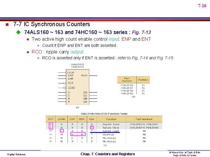
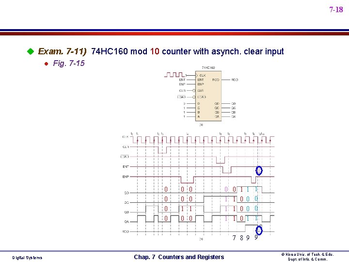
7 -16 n 7 -7 IC Synchronous Counters u 74 ALS 160 ~ 163 and 74 HC 160 ~ 163 series : Fig. 7 -13 l Two active high count enable control input: ENP and ENT » Count if ENP and ENT are both asserted. l RCO : ripple carry output » RCO is asserted only if ENT is asserted : refer to Fig. 7 -14 and Fig. 7 -15 Digital Systems Chap. 7 Counters and Registers © Korea Univ. of Tech. & Edu. Dept. of Info. & Comm.
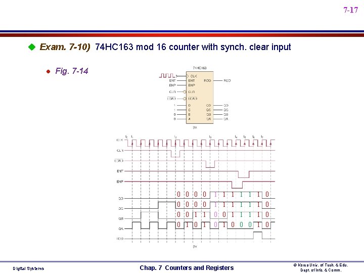
7 -17 u Exam. 7 -10) 74 HC 163 mod 16 counter with synch. clear input l Fig. 7 -14 0 0 Digital Systems 0 0 0 1 1 0 0 1 1 1 1 0 Chap. 7 Counters and Registers 1 1 1 0 0 © Korea Univ. of Tech. & Edu. Dept. of Info. & Comm.
7 -18 u Exam. 7 -11) 74 HC 160 mod 10 counter with asynch. clear input l Fig. 7 -15 0 0 0 1 1 1 0 0 0 1 1 0 0 1 7 8 9 9 Digital Systems Chap. 7 Counters and Registers © Korea Univ. of Tech. & Edu. Dept. of Info. & Comm.
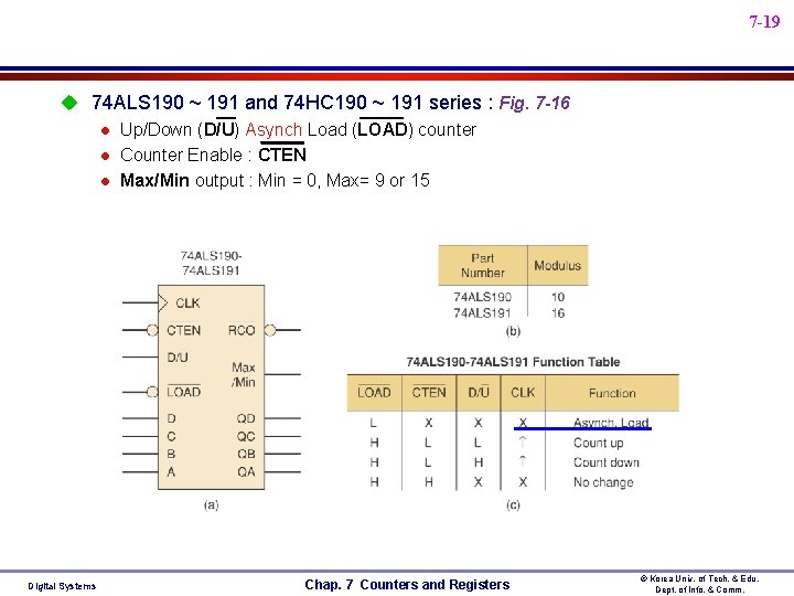
7 -19 u 74 ALS 190 ~ 191 and 74 HC 190 ~ 191 series : Fig. 7 -16 l Up/Down (D/U) Asynch Load (LOAD) counter l Counter Enable : CTEN l Max/Min output : Min = 0, Max= 9 or 15 Digital Systems Chap. 7 Counters and Registers © Korea Univ. of Tech. & Edu. Dept. of Info. & Comm.
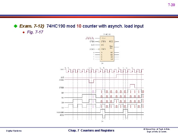
7 -20 u Exam. 7 -12) 74 HC 190 mod 10 counter with asynch. load input l Fig. 7 -17 0 1 1 1 Digital Systems 1 0 0 0 0 0 1 Chap. 7 Counters and Registers 0 0 1 0 0 0 0 1 1 0 0 1 1 1 © Korea Univ. of Tech. & Edu. Dept. of Info. & Comm.
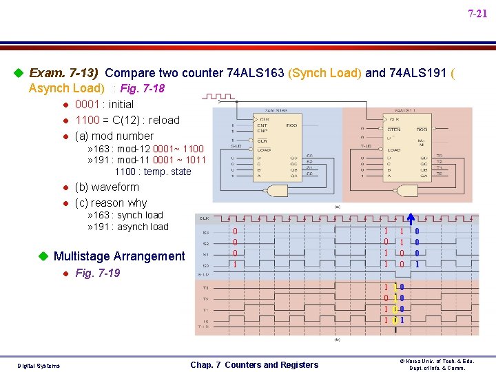
7 -21 u Exam. 7 -13) Compare two counter 74 ALS 163 (Synch Load) and 74 ALS 191 ( Asynch Load) : Fig. 7 -18 l 0001 : initial l 1100 = C(12) : reload l (a) mod number » 163 : mod-12 0001~ 1100 » 191 : mod-11 0001 ~ 1011 1100 : temp. state l l (b) waveform (c) reason why » 163 : synch load » 191 : asynch load u Multistage Arrangement l Fig. 7 -19 Digital Systems 0 0 0 1 Chap. 7 Counters and Registers 1 0 1 1 0 0 1 1 10 10 00 01 0 0 0 1 © Korea Univ. of Tech. & Edu. Dept. of Info. & Comm.
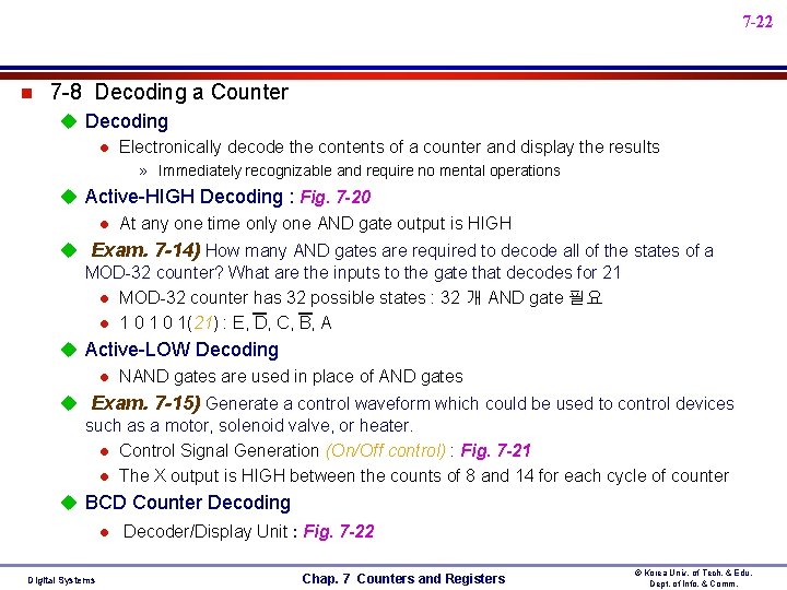
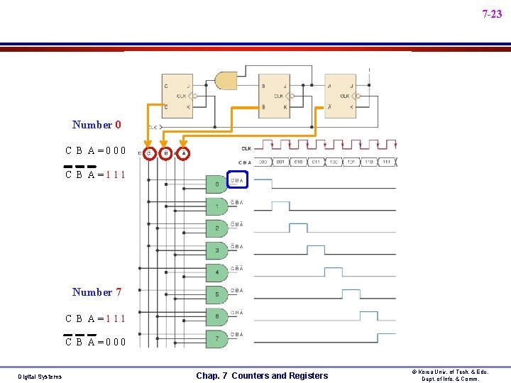
7 -22 n 7 -8 Decoding a Counter u Decoding l Electronically decode the contents of a counter and display the results » Immediately recognizable and require no mental operations u Active-HIGH Decoding : Fig. 7 -20 l At any one time only one AND gate output is HIGH u Exam. 7 -14) How many AND gates are required to decode all of the states of a MOD-32 counter? What are the inputs to the gate that decodes for 21 l MOD-32 counter has 32 possible states : 32 개 AND gate 필요 l 1 0 1(21) : E, D, C, B, A u Active-LOW Decoding l NAND gates are used in place of AND gates u Exam. 7 -15) Generate a control waveform which could be used to control devices such as a motor, solenoid valve, or heater. l Control Signal Generation (On/Off control) : Fig. 7 -21 l The X output is HIGH between the counts of 8 and 14 for each cycle of counter u BCD Counter Decoding l Digital Systems Decoder/Display Unit : Fig. 7 -22 Chap. 7 Counters and Registers © Korea Univ. of Tech. & Edu. Dept. of Info. & Comm.
7 -23 Number 0 C B A=000 C B A=111 Number 7 C B A=111 C B A=000 Digital Systems Chap. 7 Counters and Registers © Korea Univ. of Tech. & Edu. Dept. of Info. & Comm.
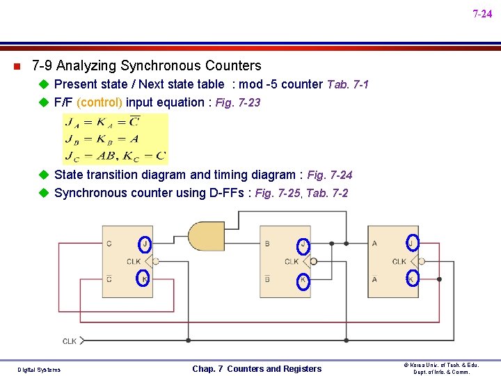
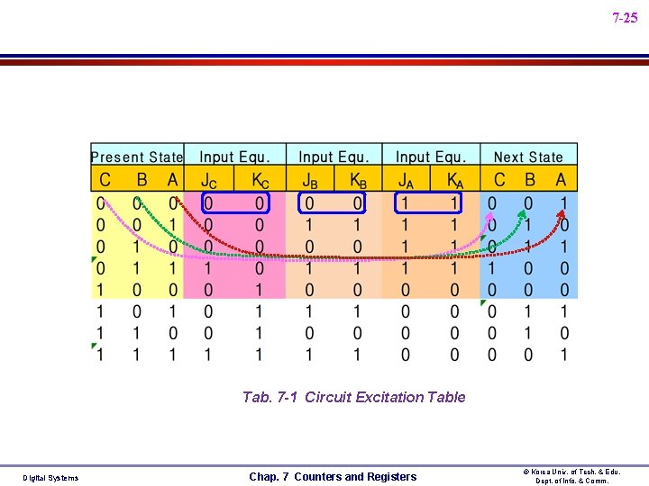
7 -24 n 7 -9 Analyzing Synchronous Counters u Present state / Next state table : mod -5 counter Tab. 7 -1 u F/F (control) input equation : Fig. 7 -23 u State transition diagram and timing diagram : Fig. 7 -24 u Synchronous counter using D-FFs : Fig. 7 -25, Tab. 7 -2 Digital Systems Chap. 7 Counters and Registers © Korea Univ. of Tech. & Edu. Dept. of Info. & Comm.
7 -25 Tab. 7 -1 Circuit Excitation Table Digital Systems Chap. 7 Counters and Registers © Korea Univ. of Tech. & Edu. Dept. of Info. & Comm.
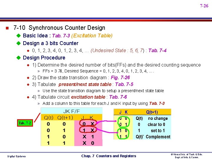
7 -26 n 7 -10 Synchronous Counter Design u Basic Idea : Tab. 7 -3 (Excitation Table) u Design a 3 bits Counter l 0, 1, 2, 3, 4, … (Undesired State : 5, 6, 7) : Tab. 7 -4 u Design Procedure l 1) Determine the desired number of bits(FFs) and the desired counting sequence » FFs = 3 개, Desired Sequence = 0, 1, 2, 3, 4, …. l l 2) Draw the state transition diagram : Fig. 7 -26 3) Tabulate present/next state table : Tab. 7 -5 » Use the state transition diagram to setup a present/next state table l 4) Tabulate circuit excitation table : Tab. 7 -6 » Add a column to this table for each J and K input by using Tab. 7 -3 Tab. 7 -2 Digital Systems Chap. 7 Counters and Registers © Korea Univ. of Tech. & Edu. Dept. of Info. & Comm.
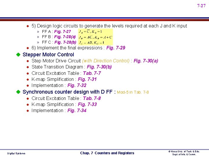
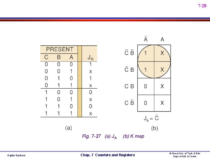
7 -27 l 5) Design logic circuits to generate the levels required at each J and K input » FF A : Fig. 7 -27 » FF B : Fig. 7 -28(a) » FF C : Fig. 7 -28(b) l 6) Implement the final expressions : Fig. 7 -29 u Stepper Motor Control l Step Motor Drive Circuit (with Direction Control) : Fig. 7 -30(a) l State Transition Diagram : Fig. 7 -30(b) l Circuit Excitation Table : Tab. 7 -7 l K-map Simplification : Fig. 7 -31 l Implementation : Fig. 7 -32 u Synchronous counter design with D FF : Mod-5 in Tab. 7 -8 l Circuit Excitation Table : Tab. 7 -8 l K-map Simplification : Fig. 7 -33 l Implementation : Fig. 7 -34 Digital Systems Chap. 7 Counters and Registers © Korea Univ. of Tech. & Edu. Dept. of Info. & Comm.
7 -28 Fig. 7 -27 (a) JA Digital Systems (b) K map Chap. 7 Counters and Registers © Korea Univ. of Tech. & Edu. Dept. of Info. & Comm.
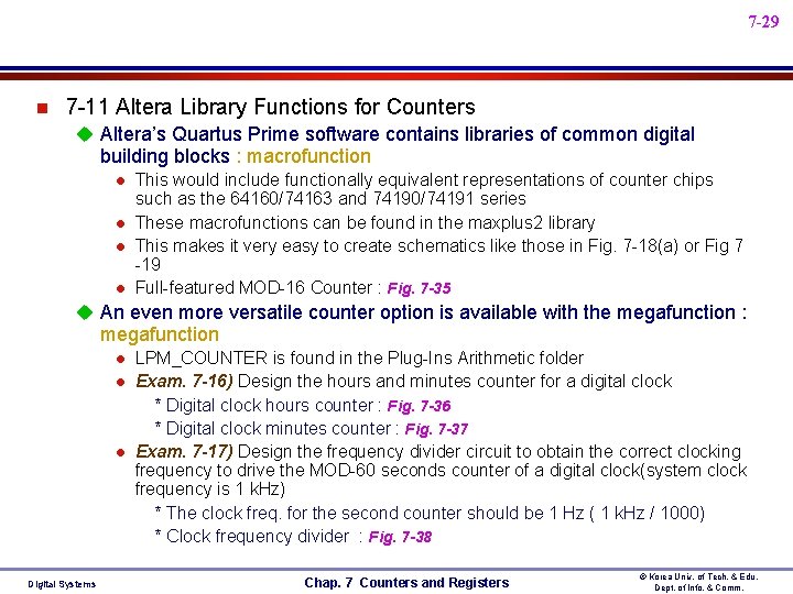
7 -29 n 7 -11 Altera Library Functions for Counters u Altera’s Quartus Prime software contains libraries of common digital building blocks : macrofunction l l This would include functionally equivalent representations of counter chips such as the 64160/74163 and 74190/74191 series These macrofunctions can be found in the maxplus 2 library This makes it very easy to create schematics like those in Fig. 7 -18(a) or Fig 7 -19 Full-featured MOD-16 Counter : Fig. 7 -35 u An even more versatile counter option is available with the megafunction : megafunction l l l Digital Systems LPM_COUNTER is found in the Plug-Ins Arithmetic folder Exam. 7 -16) Design the hours and minutes counter for a digital clock * Digital clock hours counter : Fig. 7 -36 * Digital clock minutes counter : Fig. 7 -37 Exam. 7 -17) Design the frequency divider circuit to obtain the correct clocking frequency to drive the MOD-60 seconds counter of a digital clock(system clock frequency is 1 k. Hz) * The clock freq. for the second counter should be 1 Hz ( 1 k. Hz / 1000) * Clock frequency divider : Fig. 7 -38 Chap. 7 Counters and Registers © Korea Univ. of Tech. & Edu. Dept. of Info. & Comm.
7 -30 n 7 -12 HDL Counters u State Transition Description Methods : Mod-5 Counter Fig. 7 -26 l State descriptions in AHDL : Fig. 7 -39, Fig. 7 -40(another version) l State descriptions in VHDL : Fig. 7 -41 u Behavioral Description Methods : Mod-5 Counter l The elements of a D register : Fig. 7 -42 VARIABLE l Behavioral descriptions in AHDL : Fig. 7 -43 count[3. . 0] : DFF; l Behavioral descriptions in VHDL : Fig. 7 -44 u Simulation of Basic Counter : Fig. 7 -45 n Full-featured Counters in HDL up/down, clear, load, cntenable, term_ct u 4 -bit Up/Down Counter : not exactly like a 74193, actually more similar to a 74191 How to make it count up and down : down (1=down / 0=up) How to clear it : clear How to load it : load How to enable it : cntenabl (count enable) How to include synchronous cascade controls : term_ct (terminal count) u AHDL full-featured 4 -bit Up/Down counter : Fig. 7 -46 u VHDL full-featured 4 -bit Up/Down counter : Fig. 7 -47 u Simulation of full featured counter : Fig. 7 -48 Digital Systems Chap. 7 Counters and Registers 8 bit counter 3→ 7 15 → 255 © Korea Univ. of Tech. & Edu. Dept. of Info. & Comm.
7 -31 n 7 -13 Wiring HDL Modules together u Designing large digital systems l How we can connect theses counter circuits (지금까지 설계한) to other digital modules to create larger systems. u Decoding Mod-5 Counter : Sec. 7 -8 Decoding l Decoding the AHDL Mod-5 Counter » Mod-5 counter decoder module : Fig. 7 -49 » Mod-5 counter and decoder circuit : Fig. 7 -50 circuit graphic » Simulation : Fig. 7 -51 l Decoding the VHDL Mod-5 Counter » Mod-5 counter decoder module : Fig. 7 -52 » Mod-5 counter and decoder together : Fig. 7 -53 connect toplevel program u Mod-100 BCD Counter l Cascading AHDL BCD Counters » » l Digital Systems AHDL Mod-10 BCD counter : Fig. 7 -54 Mod-10 simulation : Fig. 7 -55 Block diagram design for a Mod-100 BCD counter : Fig. 7 -56 Mod-100 simulation : Fig. 7 -57 Cascading VHDL BCD Counters : Fig. 7 -58 Chap. 7 Counters and Registers © Korea Univ. of Tech. & Edu. Dept. of Info. & Comm.
7 -32 n 7 -14 State Machines u State Machine l A circuit that sequences through a set of predetermined states. - Counter : regular numeric count sequence (used to counter events) - State machine : irregular counting pattern like our stepper motor control (used to control events) u Block diagram for counters and state machines : Fig. 7 -59 l Mealy model : Mod-100 BCD circuit Fig. 7 -56 » Output signals are also controlled by additional input signals (enable, clear) » Output signals can have asynchronous changes » Mealy model has control inputs for outputs l Moore model : Mod-5 circuit Fig. 7 -50 » Output signals are not controlled by additional input signals (the output is a function only of the current flip-flop state). » Output signals are all synchronous to circuit’s clock » Moore model has no control inputs for outputs Digital Systems Chap. 7 Counters and Registers © Korea Univ. of Tech. & Edu. Dept. of Info. & Comm.
7 -33 u Simple state machine : Washing machine states l Idle : until the start button is pressed l Fill : fill with water until the tub is full l Agitate : agitate the tub until a timer expires l Spin : spin the tub until the water is spun out, at which time it goes back to idle. u Simple AHDL state machines : Fig. 7 -60 u Simple VHDL state machines : Fig. 7 -61 u Simulation of washing machine : Fig. 7 -62 u Traffic Light Controller State Machine l Traffic light controller : Fig. 7 -63 l AHDL traffic light controller : Fig. 7 -64 l VHDL traffic light controller : Fig. 7 -65 Digital Systems Chap. 7 Counters and Registers © Korea Univ. of Tech. & Edu. Dept. of Info. & Comm.
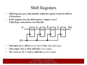
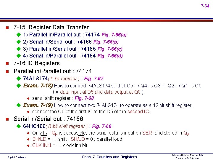
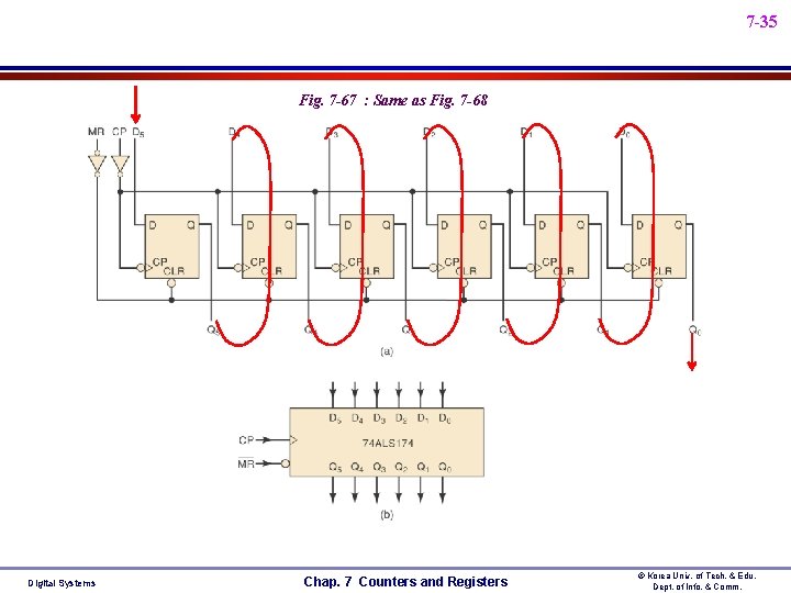
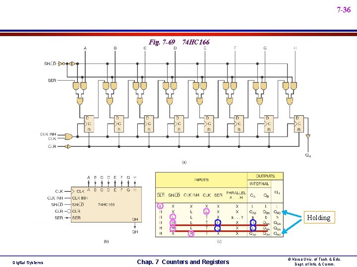
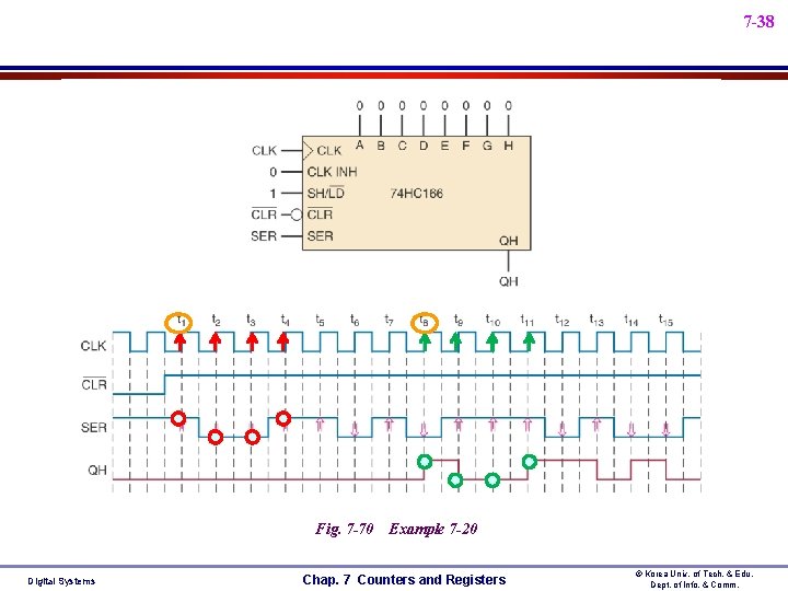
7 -34 n 7 -15 Register Data Transfer u u n n 1) Parallel in/Parallel out : 74174 Fig. 7 -66(a) 2) Serial in/Serial out : 74166 Fig. 7 -66(b) 3) Parallel in/Serial out : 74165 Fig. 7 -66(c) 4) Serial in/Parallel out : 74164 Fig. 7 -66(d) 7 -16 IC Registers Parallel in/Parallel out : 74174 u 74 ALS 174( 6 bit register ) : Fig. 7 -67 u Exam. 7 -18) How to connect 74 ALS 174 so that Q 5 Q 4 Q 3 Q 2 Q 1 Q 0 ( = data input at D 5 and data output at Q 0 ). l serial shift register : Fig. 7 -68 u Exam. 7 -19) How to connect two 74 ALS 174 to operate as a 12 bit shift register. l connect the Q 0 of the first IC to the D 5 of the second IC. n Serial in/Serial out : 74166 u 64 HC 166( 8 -bit shift register ) : Fig. 7 -69 l Only F/F QH is accessible, the serial data is input on SER, and stored in QA l SH/LD = 1 : shift , SH/LD = 0 : parallel load l CLK INH = 1 : clock inhibit Digital Systems Chap. 7 Counters and Registers © Korea Univ. of Tech. & Edu. Dept. of Info. & Comm.
7 -35 Fig. 7 -67 : Same as Fig. 7 -68 Digital Systems Chap. 7 Counters and Registers © Korea Univ. of Tech. & Edu. Dept. of Info. & Comm.
7 -36 Fig. 7 -69 74 HC 166 Holding Digital Systems Chap. 7 Counters and Registers © Korea Univ. of Tech. & Edu. Dept. of Info. & Comm.
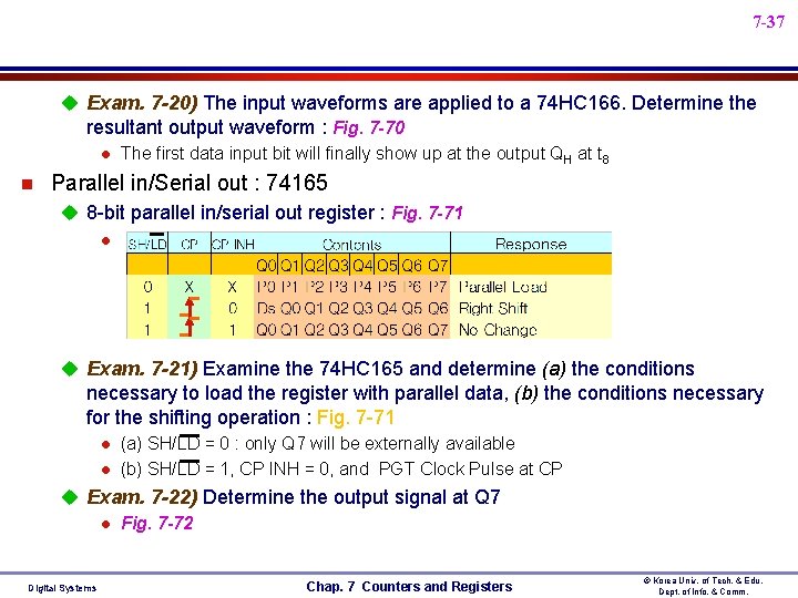
7 -37 u Exam. 7 -20) The input waveforms are applied to a 74 HC 166. Determine the resultant output waveform : Fig. 7 -70 l The first data input bit will finally show up at the output Q H at t 8 n Parallel in/Serial out : 74165 u 8 -bit parallel in/serial out register : Fig. 7 -71 l Truth Table u Exam. 7 -21) Examine the 74 HC 165 and determine (a) the conditions necessary to load the register with parallel data, (b) the conditions necessary for the shifting operation : Fig. 7 -71 l l (a) SH/LD = 0 : only Q 7 will be externally available (b) SH/LD = 1, CP INH = 0, and PGT Clock Pulse at CP u Exam. 7 -22) Determine the output signal at Q 7 l Fig. 7 -72 Digital Systems Chap. 7 Counters and Registers © Korea Univ. of Tech. & Edu. Dept. of Info. & Comm.
7 -38 Fig. 7 -70 Digital Systems Example 7 -20 Chap. 7 Counters and Registers © Korea Univ. of Tech. & Edu. Dept. of Info. & Comm.
7 -39 Fig. 7 -72 Q 0 Example 7 -22 Q 7 Q 0 1 0 Digital Systems Q 7 0 1 0 1 0 0 0 1 0 1 0 1 1 0 0 Chap. 7 Counters and Registers 1 0 1 1 0 0 © Korea Univ. of Tech. & Edu. Dept. of Info. & Comm. 1
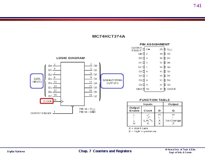
7 -40 n Serial in/Parallel out : 74 ALS 164 / 74 HC 164 u 8 -bit serial in/parallel out shift register : Fig. 7 -73 l Each FF output externally accessible : Q 0, Q 1, …, Q 7 l 2 input AND gate (A and B) : one input can be used for control u Exam. 7 -23) Determine the sequence of states in Fig. 7 -74(a) (Initial Content of the 74 ALS 164 = 0000) l The correct sequence : Fig. 7 -74(b) » Q 7 =1 : Temporary state n n LOW at MR ( inverted Q 7 ) resets the register back to 0000 Other Register ICs u 74194/LS 194/HC 194 : 4 bit bi-directional universal shift register l 4 mode : shift left, shift right, parallel in, parallel out ( selected by 2 bit mode select code as inputs ) u 74373/LS 373/HC 373 : 8 bit parallel in/parallel out register l 8 D latch with tri-state outputs : Data or Address buffer로 주로 사용됨 » Pin 11 : Latch Enable (LE)로 Level trigger = 1 일 때 8 개 입력 D 0 - D 7 이 8 개 출력 Q 0 - Q 7으로 출력됨(따라서 Transparent Latch 라고도 함) u 74374/LS 374/HC 374 : 8 bit parallel in/parallel out register l 8 edge-triggered D Flip-Flops with tri-state outputs » Pin 11 : Clock Pulse (CP)로 Edge trigger(PGT) 일 때 373과 마찬가지로 출력됨 Digital Systems Chap. 7 Counters and Registers © Korea Univ. of Tech. & Edu. Dept. of Info. & Comm.
7 -41 Digital Systems Chap. 7 Counters and Registers © Korea Univ. of Tech. & Edu. Dept. of Info. & Comm.
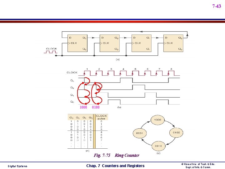
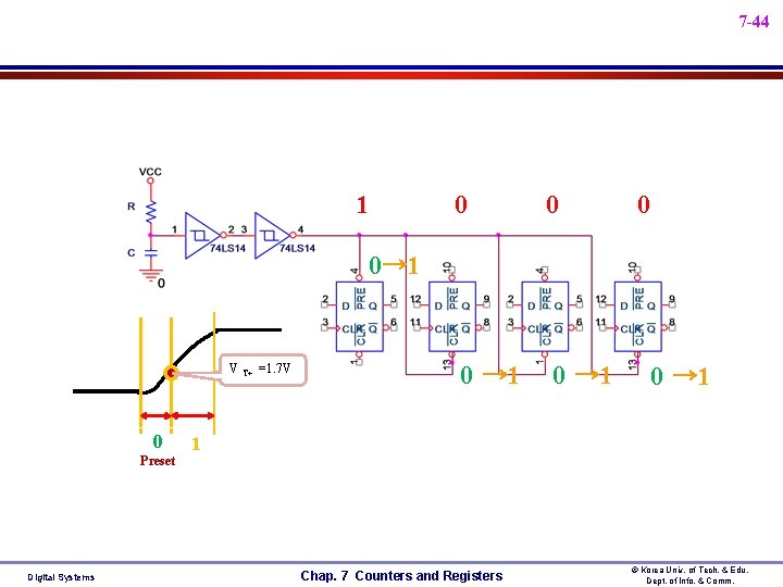
7 -42 n 7 -17 Shift-Register Counters u Shift-Register l Transfer data left to right, or vice versa, one bit at a time (serially) l Shift-register counters use feedback : Fig. 7 -75(a), Fig. 7 -77(a) » the output of the last FF in the register is connected back to the first FF in some way u Ring Counter l In most instances only a single 1 is in the register 4 distinct states l MOD-4 Ring Counter : Fig. 7 -75 » Ring counters can be constructed for any desired MOD number n A MOD-N ring counter used N flip-flops u Starting a Ring Counter l A ring counter must start off with only one FF in the 1 state and all the others in the 0 state l Ring Counter Starter : Fig. 7 -76 » 1) On power-up, the capacitor will charge up relatively slowly toward Vcc, 따라서 Inverter 1 input = 0 » 2) Inverter 1 output = 1, 따라서 Inverter 2 output = 0 until Inverter 1 input = 1 n Digital Systems 이때 Q 3 = PRE, Q 2 = Q 1 = Q 0 = CLR 임으로 1 0 0 0 으로 Preset 됨 Chap. 7 Counters and Registers © Korea Univ. of Tech. & Edu. Dept. of Info. & Comm.
7 -43 1000 0100 Fig. 7 -75 Digital Systems Ring Counter Chap. 7 Counters and Registers © Korea Univ. of Tech. & Edu. Dept. of Info. & Comm.
7 -44 1 0 0 0 → 1 0 0→ 1 V T+ =1. 7 V 0 Preset Digital Systems 0 → 1 1 Chap. 7 Counters and Registers © Korea Univ. of Tech. & Edu. Dept. of Info. & Comm.
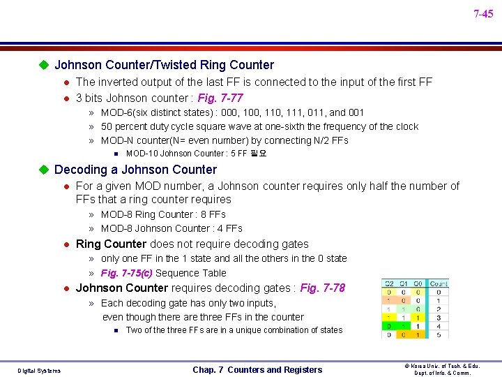
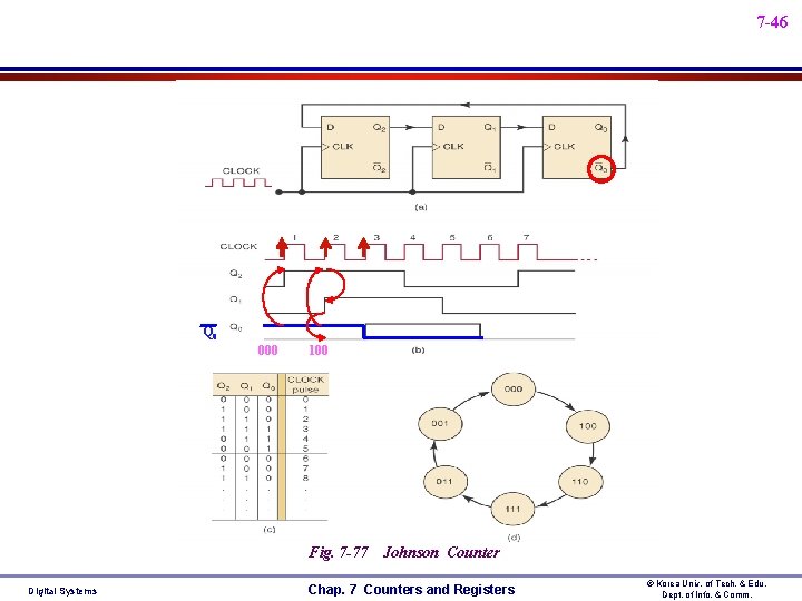
7 -45 u Johnson Counter/Twisted Ring Counter l The inverted output of the last FF is connected to the input of the first FF l 3 bits Johnson counter : Fig. 7 -77 » MOD-6(six distinct states) : 000, 110, 111, 011, and 001 » 50 percent duty cycle square wave at one-sixth the frequency of the clock » MOD-N counter(N= even number) by connecting N/2 FFs n MOD-10 Johnson Counter : 5 FF 필요 u Decoding a Johnson Counter l For a given MOD number, a Johnson counter requires only half the number of FFs that a ring counter requires » MOD-8 Ring Counter : 8 FFs » MOD-8 Johnson Counter : 4 FFs l Ring Counter does not require decoding gates » only one FF in the 1 state and all the others in the 0 state » Fig. 7 -75(c) Sequence Table l Johnson Counter requires decoding gates : Fig. 7 -78 » Each decoding gate has only two inputs, even though there are three FFs in the counter n Digital Systems Two of the three FFs are in a unique combination of states Chap. 7 Counters and Registers © Korea Univ. of Tech. & Edu. Dept. of Info. & Comm.
7 -46 Q 0 000 100 Fig. 7 -77 Digital Systems Johnson Counter Chap. 7 Counters and Registers © Korea Univ. of Tech. & Edu. Dept. of Info. & Comm.
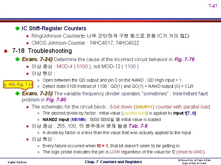
7 -47 u IC Shift-Register Counters l Ring/Johnson Counter는 너무 간단하게 구현 됨으로 전용 IC가 거의 없다 l CMOS Johnson-Counter : 74 HC 4017, 74 HC 4022 n 7 -18 Troubleshooting u Exam. 7 -24) Determine the cause of the incorrect circuit behavior in Fig. 7 -79 l 이상 증상 : MOD-4 ( 0100 ), not MOD-12 ( 1100 ) l 이상 원인 : » Open between the QD output and pin 2 on the NAND : QD High input = 1 p. 400, Fig. 7 -16 » Detect state 0100 instead of 1100 : QD(1) and QC(1) = NAND output (0) = CLR u Exam. 7 -25) The variable frequency divider operates “sometimes” : Intermittent fault problem in Fig. 7 -80 l The schematic for the circuit block : 8 -bit down (DNUP=1) counter with parallel load » The desired divide-by factor : initial value (parallel load) is applied to input f[7. . 0] » NAND 2 input (MXMN) : 0000일 때 initial value is loaded l 이상 증상 : 255, 100, 15 분주에서 문제 발생 Tab. 7 -9 » A divide-by factor is 4 less than the value that was actually applied to the input. l 이상 원인 : » Every failure occurred when f 2 = 1, that bit doesn’t seem to be getting in. » The logic probe indicates the pin is LOW regardless of the value for f 2 (short to GND). Digital Systems Chap. 7 Counters and Registers © Korea Univ. of Tech. & Edu. Dept. of Info. & Comm.
7 -48 n 7 -19 Megafunction Registers u Quartus Prime maxplus 2 library also contains functionally equivalent u u Digital Systems versions of “old-style” MSI register chips such as the examples discussed in Section 7 -16 (macrofunction) A much easier schematic option for implementing registers in designs is available with the megafunction Megafunction LPM_SHIFTREG is found in the Mega. Wizard Manager’s Plug-Ins Storage folder(now Tools “IP Catalog”) Multipurpose Shift Register : Fig. 7 -81 Exam. 7 -26) Design a MOD-5 ring counter using LPM_SHIFTREG (restart at 10000) : Fig. 7 -82 Chap. 7 Counters and Registers © Korea Univ. of Tech. & Edu. Dept. of Info. & Comm.
7 -49 n 7 -20 HDL Registers u Data transfer mode in shift registers : Fig. 7 -83 l parallel load, shift right, shift left, and hold u AHDL SISO shift register : Fig. 7 -84 SISO register simulation : Fig. 7 -85 u VHDL SISO shift register : Fig. 7 -86 u AHDL PISO register : Fig. 7 -87 PISO register simulation : Fig. 7 -88 u VHDL PISO register : Fig. 7 -89 u Exam. 7 -27) Design of a universal 4 bit shift register. Requirements are: l 4 synchronous modes of operation: hold, shift left, shift right, and parallel load l 2 input bits (mode selection) select the operation to be performed - AHDL 4 bit universal shift register solution : Fig. 7 -90 - VHDL 4 bit universal shift register solution : Fig. 7 -91 n 7 -21 HDL Ring Counters u a ring counter is a shift register that circulates a single active logic level through all its FFs. u AHDL 4 bit ring counter : Fig. 7 -92 Ring counter simulation : Fig. 7 -93 u VHDL 4 bit ring counter : Fig. 7 -94 Digital Systems Chap. 7 Counters and Registers © Korea Univ. of Tech. & Edu. Dept. of Info. & Comm.
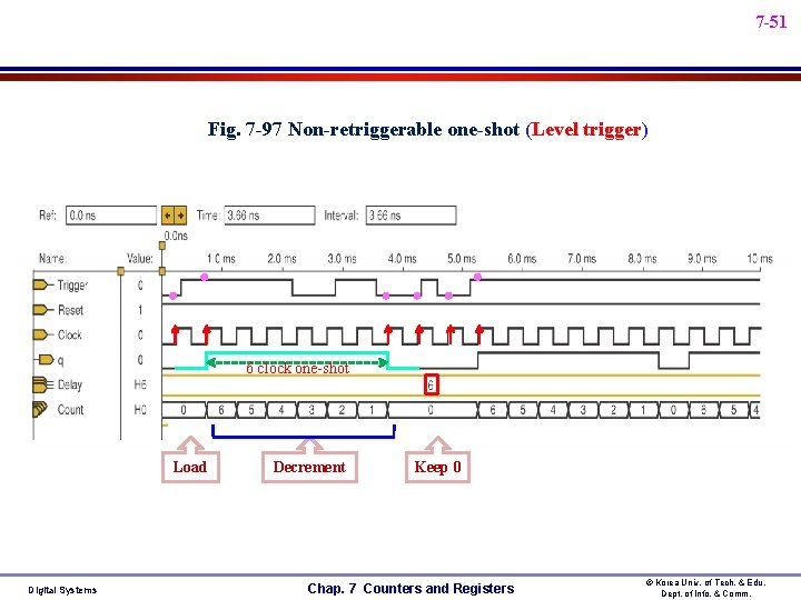
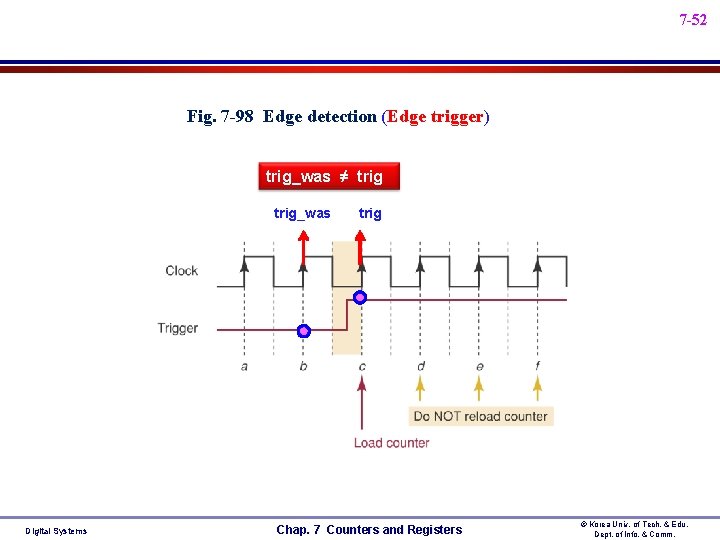
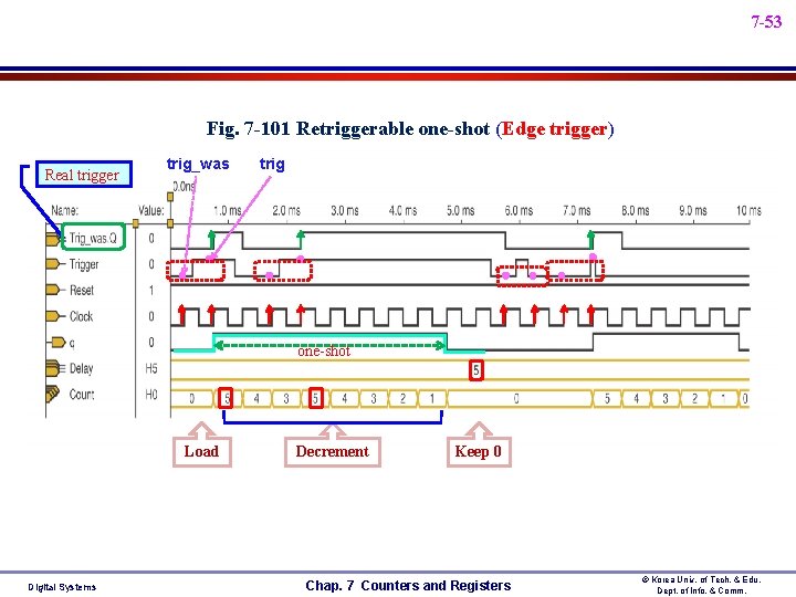
7 -50 n 7 -22 HDL One-Shots u One-Shots l 74121 + RC one-shots : Chap. 5 -21 l HDL one-shots : in this Chap » A 4 -bit counter to determine the width of the pulse. u Non-retriggerable Simple One-Shot : level triggered l AHDL solution : Fig. 7 -95 l VHDL solution : Fig. 7 -96 l Simulation of the nonretriggerable on-shots : Fig. 7 -97 u Retriggerable One-Shot : edge triggered l Detecting edges : Fig. 7 -98 » trigger ( c ) = 1 AND trigger_was ( b ) = 0 l When a clock edge occurs, one of three conditions exists: » 1. Load counter : line 17 / 16 » 2. Keep it at zero (when counter = 0) : line 18 / 18 » 3. Count down by 1 (when counter ≠ 0) : line 19 / 19 l l l Digital Systems AHDL solution : Fig. 7 -99 ( line 17, 18, 19 ) VHDL solution : Fig. 7 -100 ( line 16, 18, 19 ) Simulation of the edge-triggered retriggerable on-shots : Fig. 7 -101 Chap. 7 Counters and Registers © Korea Univ. of Tech. & Edu. Dept. of Info. & Comm.
7 -51 Fig. 7 -97 Non-retriggerable one-shot (Level trigger) 6 clock one-shot Load Digital Systems Decrement Keep 0 Chap. 7 Counters and Registers © Korea Univ. of Tech. & Edu. Dept. of Info. & Comm.
7 -52 Fig. 7 -98 Edge detection (Edge trigger) trig_was ≠ trig_was Digital Systems trig Chap. 7 Counters and Registers © Korea Univ. of Tech. & Edu. Dept. of Info. & Comm.
7 -53 Fig. 7 -101 Retriggerable one-shot (Edge trigger) Real trigger trig_was trig one-shot Load Digital Systems Decrement Keep 0 Chap. 7 Counters and Registers © Korea Univ. of Tech. & Edu. Dept. of Info. & Comm.