146 CHAPTER 12 REGISTERS AND COUNTERS This chapter




- Slides: 46

1/46 CHAPTER 12 REGISTERS AND COUNTERS This chapter in the book includes: Objectives Study Guide 12. 1 Registers and Register Transfers 12. 2 Shift Registers 12. 3 Design of Binary Counters 12. 4 Counters for Other Sequences 12. 5 Counter Design Using S-R and J-K Flip-Flops 12. 6 Derivation of Flip-Flop Input Equations--Summary Problems Fundamentals of Logic Design

2/46 Objectives Topics introduced in this chapter: 1. Explain the operation of registers. Understand how to transfer data between registers using tri-state bus. 2. Explain the shift register operation, how to build them and analyze operation. Construct a timing diagram for a shift register 3. Explain the operation of binary counters, how to build them using F/F and gates and analyze operation. 4. Given the present state and desired next state of F/F, determine the required F/F/ inputs 5. Given the desired counting sequence for a counter, derive F/F input equations. 6. Explain the procedures used for deriving F/F input equation. 7. Construct a timing diagram for a counter by tracing signals through the circuit. Fundamentals of Logic Design

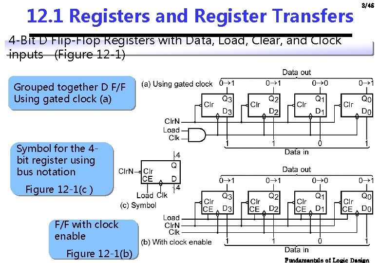
12. 1 Registers and Register Transfers 3/46 4 -Bit D Flip-Flop Registers with Data, Load, Clear, and Clock inputs (Figure 12 -1) Grouped together D F/F Using gated clock (a) Symbol for the 4 bit register using bus notation Figure 12 -1(c ) F/F with clock enable Figure 12 -1(b) Fundamentals of Logic Design

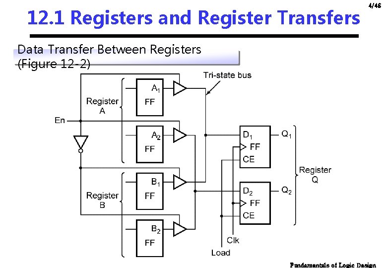
12. 1 Registers and Register Transfers 4/46 Data Transfer Between Registers (Figure 12 -2) Fundamentals of Logic Design

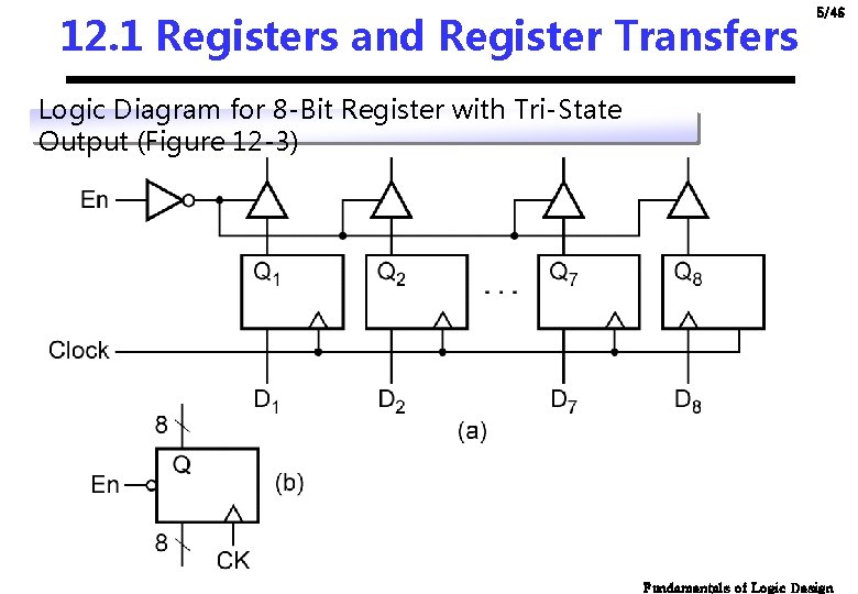
12. 1 Registers and Register Transfers 5/46 Logic Diagram for 8 -Bit Register with Tri-State Output (Figure 12 -3) Fundamentals of Logic Design

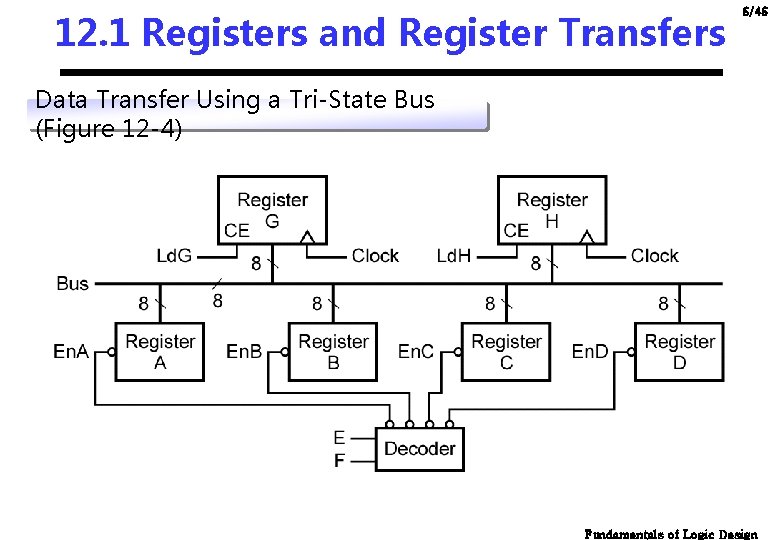
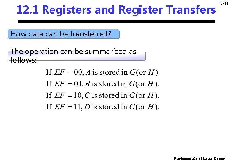
12. 1 Registers and Register Transfers 6/46 Data Transfer Using a Tri-State Bus (Figure 12 -4) Fundamentals of Logic Design

12. 1 Registers and Register Transfers 7/46 How data can be transferred? The operation can be summarized as follows: Fundamentals of Logic Design

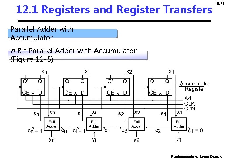
12. 1 Registers and Register Transfers 8/46 Parallel Adder with Accumulator n-Bit Parallel Adder with Accumulator (Figure 12 -5) Fundamentals of Logic Design

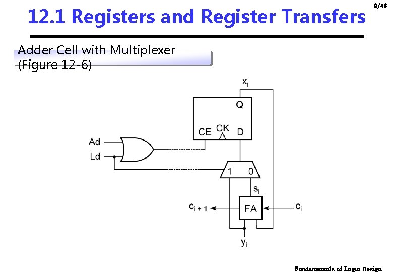
12. 1 Registers and Register Transfers 9/46 Adder Cell with Multiplexer (Figure 12 -6) Fundamentals of Logic Design

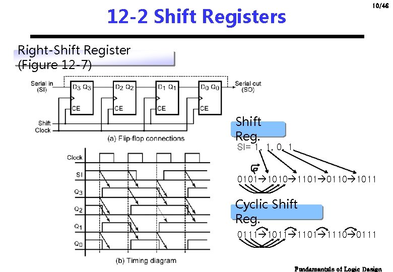
10/46 12 -2 Shift Registers Right-Shift Register (Figure 12 -7) Shift Reg. SI= 1, 1, 0, 1 0101 1010 1101 0110 1011 Cyclic Shift Reg. 0111 1011 1101 1110 0111 Fundamentals of Logic Design

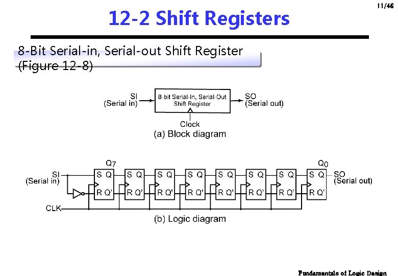
12 -2 Shift Registers 11/46 8 -Bit Serial-in, Serial-out Shift Register (Figure 12 -8) Fundamentals of Logic Design

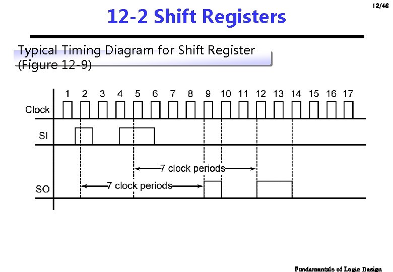
12 -2 Shift Registers 12/46 Typical Timing Diagram for Shift Register (Figure 12 -9) Fundamentals of Logic Design

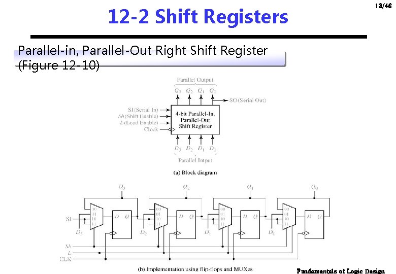
12 -2 Shift Registers 13/46 Parallel-in, Parallel-Out Right Shift Register (Figure 12 -10) Fundamentals of Logic Design

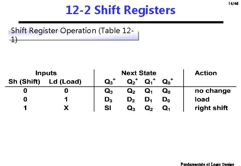
12 -2 Shift Registers 14/46 Shift Register Operation (Table 121) Fundamentals of Logic Design

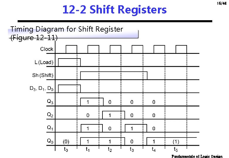
12 -2 Shift Registers 15/46 Timing Diagram for Shift Register (Figure 12 -11) Fundamentals of Logic Design

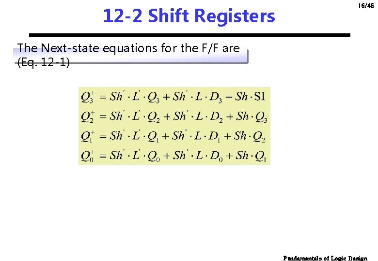
12 -2 Shift Registers 16/46 The Next-state equations for the F/F are (Eq. 12 -1) Fundamentals of Logic Design

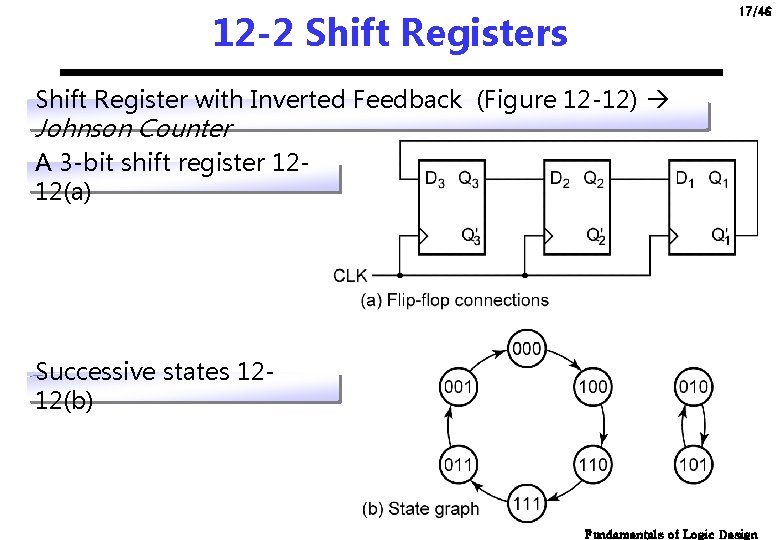
17/46 12 -2 Shift Registers Shift Register with Inverted Feedback (Figure 12 -12) Johnson Counter A 3 -bit shift register 1212(a) Successive states 1212(b) Fundamentals of Logic Design

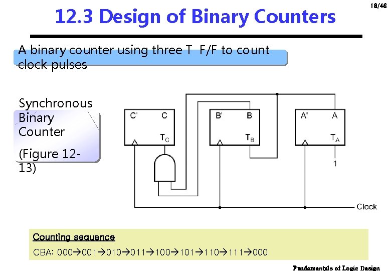
12. 3 Design of Binary Counters 18/46 A binary counter using three T F/F to count clock pulses Synchronous Binary Counter (Figure 1213) Counting sequence CBA: 000 001 010 011 100 101 110 111 000 Fundamentals of Logic Design

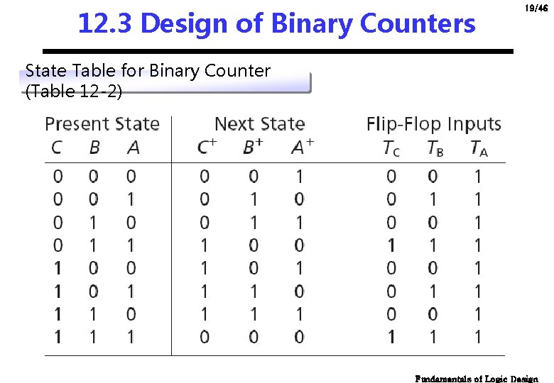
12. 3 Design of Binary Counters 19/46 State Table for Binary Counter (Table 12 -2) Fundamentals of Logic Design

12. 3 Design of Binary Counters 20/46 Karnaugh Map for Binary Counter (Figure 12 -14) TA=1, TB=A, TC=AB Fundamentals of Logic Design

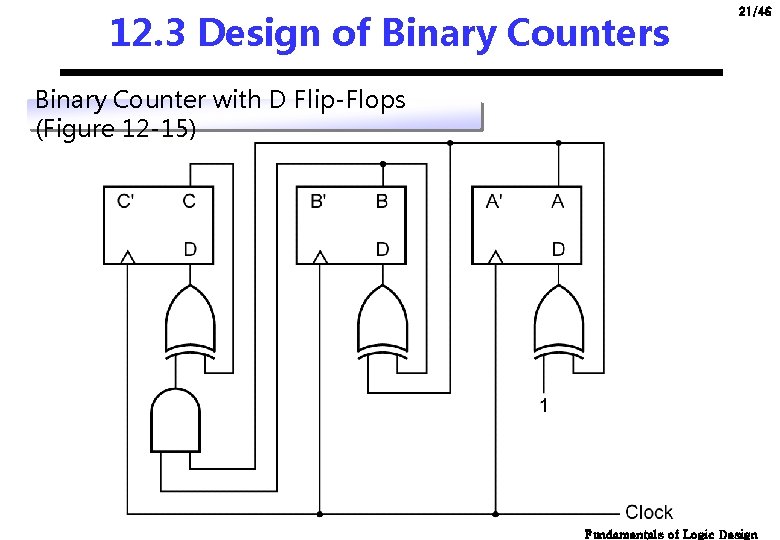
12. 3 Design of Binary Counters 21/46 Binary Counter with D Flip-Flops (Figure 12 -15) Fundamentals of Logic Design

12. 3 Design of Binary Counters 22/46 The D input equations derived from the maps are (Eq. 12 -2) Karnaugh Maps for D Flip-Flops (Figure 12 -16) Fundamentals of Logic Design

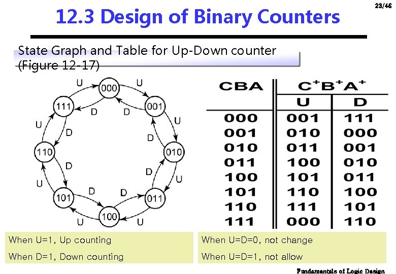
12. 3 Design of Binary Counters 23/46 State Graph and Table for Up-Down counter (Figure 12 -17) When U=1, Up counting When U=D=0, not change When D=1, Down counting When U=D=1, not allow Fundamentals of Logic Design

12. 3 Design of Binary Counters 24/46 The up-down counter can be implemented using D F/F and gate Binary Up. Down Counter (Figure 1218) Fundamentals of Logic Design

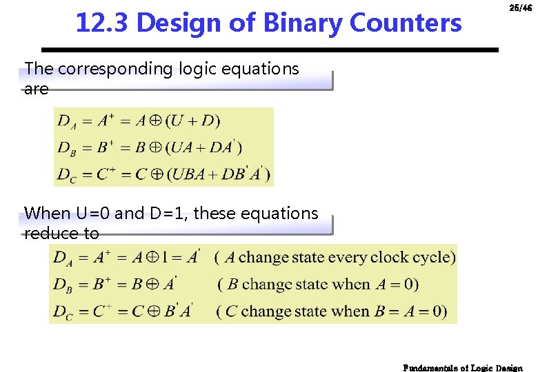
12. 3 Design of Binary Counters 25/46 The corresponding logic equations are When U=0 and D=1, these equations reduce to Fundamentals of Logic Design

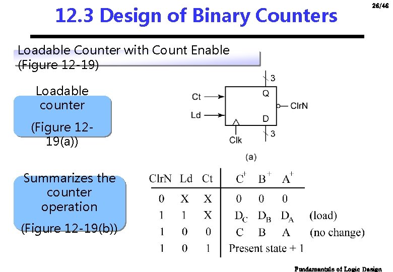
12. 3 Design of Binary Counters 26/46 Loadable Counter with Count Enable (Figure 12 -19) Loadable counter (Figure 1219(a)) Summarizes the counter operation (Figure 12 -19(b)) Fundamentals of Logic Design

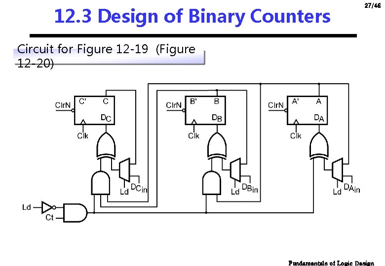
12. 3 Design of Binary Counters 27/46 Circuit for Figure 12 -19 (Figure 12 -20) Fundamentals of Logic Design

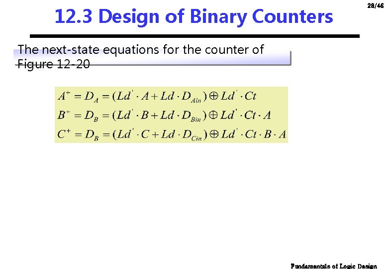
12. 3 Design of Binary Counters 28/46 The next-state equations for the counter of Figure 12 -20 Fundamentals of Logic Design

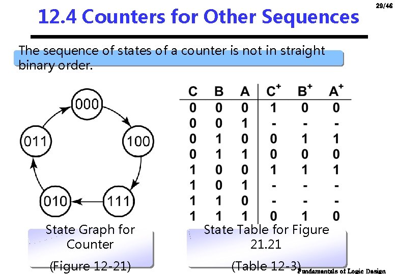
12. 4 Counters for Other Sequences 29/46 The sequence of states of a counter is not in straight binary order. State Graph for Counter (Figure 12 -21) State Table for Figure 21. 21 (Table 12 -3)Fundamentals of Logic Design

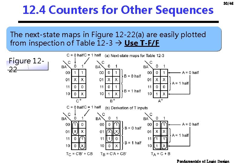
12. 4 Counters for Other Sequences 30/46 The next-state maps in Figure 12 -22(a) are easily plotted from inspection of Table 12 -3 Use T-F/F Figure 1222 Fundamentals of Logic Design

12. 4 Counters for Other Sequences 31/46 Input for T Flip. Flop (Table 12 -4) Counter Using T Flip -Flops (Figure 1223) Fundamentals of Logic Design

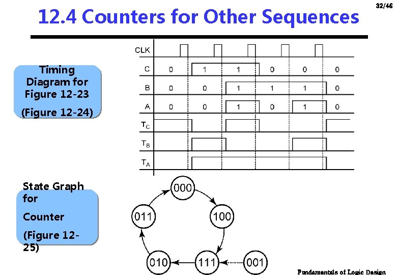
12. 4 Counters for Other Sequences 32/46 Timing Diagram for Figure 12 -23 (Figure 12 -24) State Graph for Counter (Figure 1225) Fundamentals of Logic Design

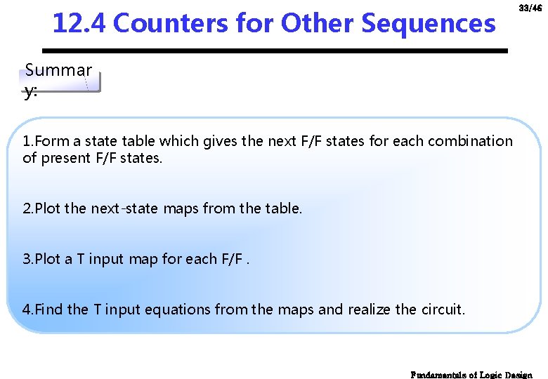
12. 4 Counters for Other Sequences 33/46 Summar y: 1. Form a state table which gives the next F/F states for each combination of present F/F states. 2. Plot the next-state maps from the table. 3. Plot a T input map for each F/F. 4. Find the T input equations from the maps and realize the circuit. Fundamentals of Logic Design

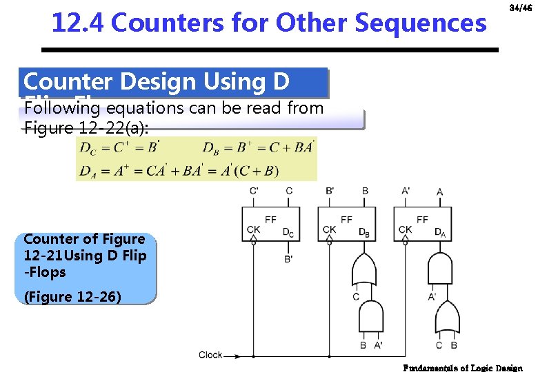
12. 4 Counters for Other Sequences 34/46 Counter Design Using D Flip-Flop Following equations can be read from Figure 12 -22(a): Counter of Figure 12 -21 Using D Flip -Flops (Figure 12 -26) Fundamentals of Logic Design

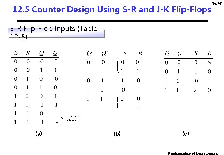
12. 5 Counter Design Using S-R and J-K Flip-Flops 35/46 S-R Flip-Flop Inputs (Table 12 -5) Inputs not allowed (a) (b) (c) Fundamentals of Logic Design

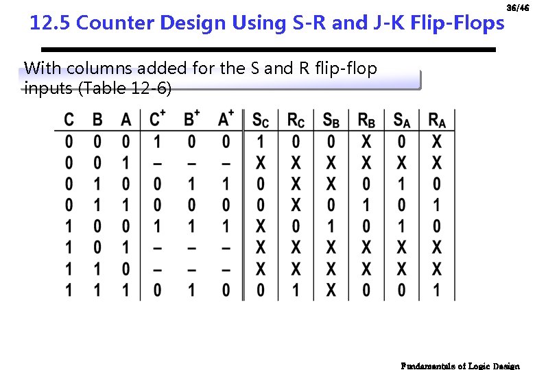
12. 5 Counter Design Using S-R and J-K Flip-Flops 36/46 With columns added for the S and R flip-flop inputs (Table 12 -6) Fundamentals of Logic Design

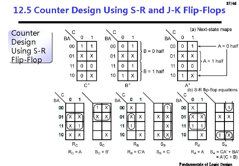
12. 5 Counter Design Using S-R and J-K Flip-Flops 37/46 Counter Design Using S-R Flip-Flop Fundamentals of Logic Design

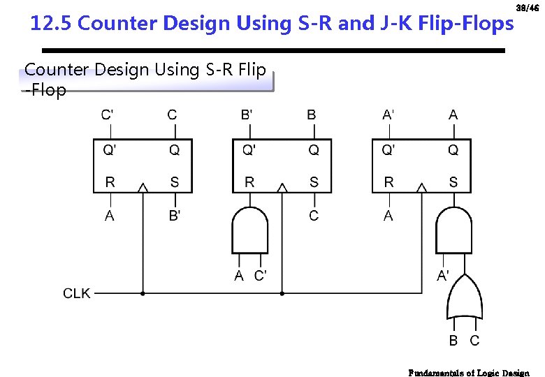
12. 5 Counter Design Using S-R and J-K Flip-Flops 38/46 Counter Design Using S-R Flip -Flop Fundamentals of Logic Design

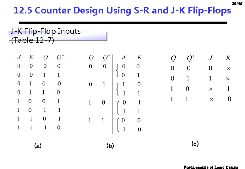
12. 5 Counter Design Using S-R and J-K Flip-Flops 39/46 J-K Flip-Flop Inputs (Table 12 -7) (a) (b) (c) Fundamentals of Logic Design

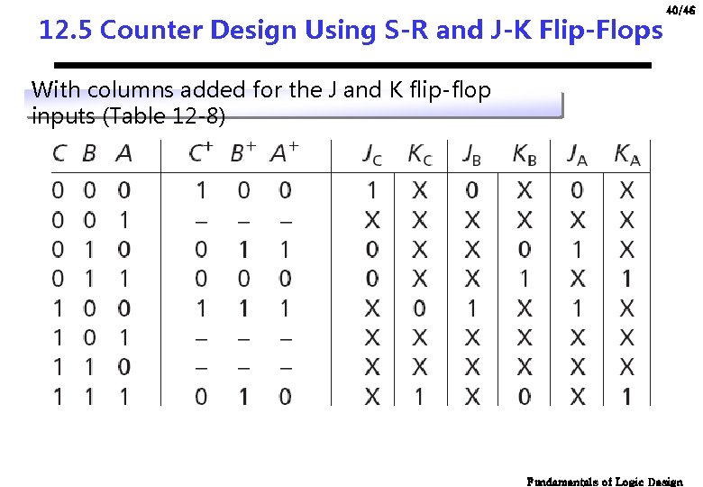
12. 5 Counter Design Using S-R and J-K Flip-Flops 40/46 With columns added for the J and K flip-flop inputs (Table 12 -8) Fundamentals of Logic Design

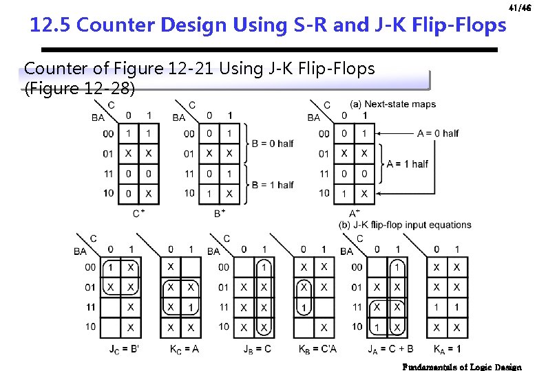
12. 5 Counter Design Using S-R and J-K Flip-Flops 41/46 Counter of Figure 12 -21 Using J-K Flip-Flops (Figure 12 -28) Fundamentals of Logic Design

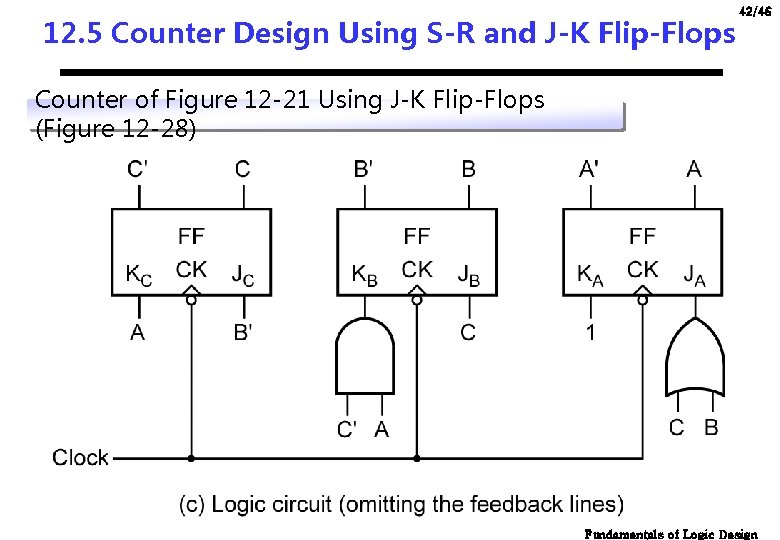
12. 5 Counter Design Using S-R and J-K Flip-Flops 42/46 Counter of Figure 12 -21 Using J-K Flip-Flops (Figure 12 -28) Fundamentals of Logic Design

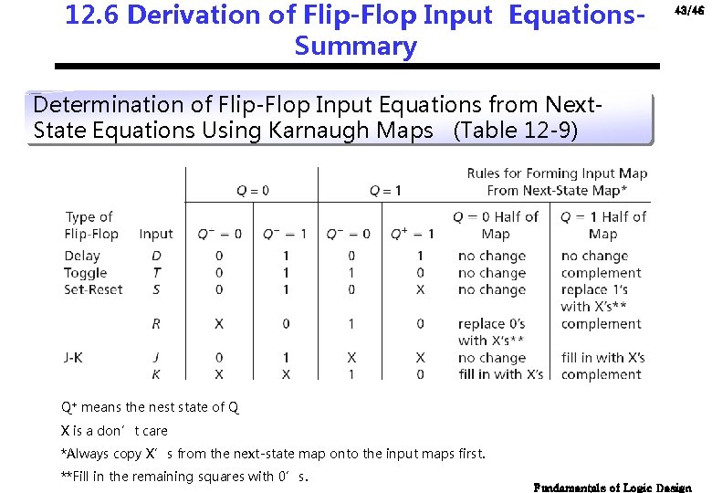
12. 6 Derivation of Flip-Flop Input Equations. Summary 43/46 Determination of Flip-Flop Input Equations from Next. State Equations Using Karnaugh Maps (Table 12 -9) Q+ means the nest state of Q X is a don’t care *Always copy X’s from the next-state map onto the input maps first. **Fill in the remaining squares with 0’s. Fundamentals of Logic Design

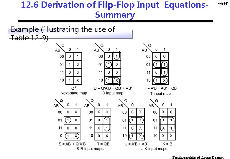
12. 6 Derivation of Flip-Flop Input Equations. Summary 44/46 Example (illustrating the use of Table 12 -9) Fundamentals of Logic Design

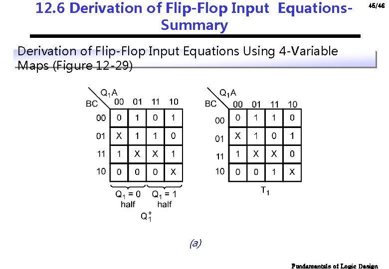
12. 6 Derivation of Flip-Flop Input Equations. Summary 45/46 Derivation of Flip-Flop Input Equations Using 4 -Variable Maps (Figure 12 -29) (a) Fundamentals of Logic Design

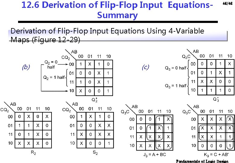
12. 6 Derivation of Flip-Flop Input Equations. Summary 46/46 Derivation of Flip-Flop Input Equations Using 4 -Variable Maps (Figure 12 -29) (b) (c) Fundamentals of Logic Design