CHAPTER 6 OPTICAL AMPLIFIERS Why Optical Amplifiers Increase

- Slides: 40

CHAPTER 6 OPTICAL AMPLIFIERS

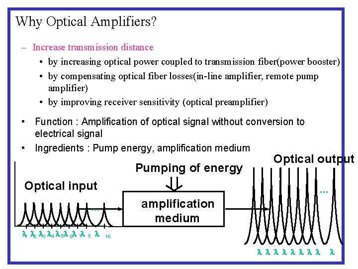
Why Optical Amplifiers? – Increase transmission distance • by increasing optical power coupled to transmission fiber(power booster) • by compensating optical fiber losses(in-line amplifier, remote pump amplifier) • by improving receiver sensitivity (optical preamplifier) • Function : Amplification of optical signal without conversion to electrical signal • Ingredients : Pump energy, amplification medium Pumping of energy Optical input . . . amplification medium . . . 1 2 3 4 5 6 7 8 Optical output 16

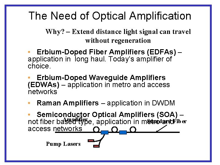
The Need of Optical Amplification Why? – Extend distance light signal can travel without regeneration • Erbium-Doped Fiber Amplifiers (EDFAs) – application in long haul. Today’s amplifier of choice. • Erbium-Doped Waveguide Amplifiers (EDWAs) – application in metro and access networks • Raman Amplifiers – application in DWDM • Semiconductor Optical Amplifiers (SOA) – Amplifier Standard not fiber based type, application in metro and. Fiber access networks Pump Lasers

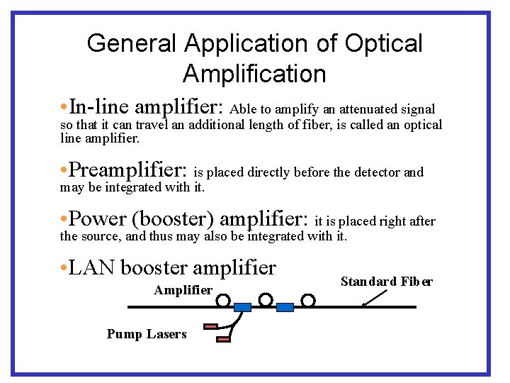
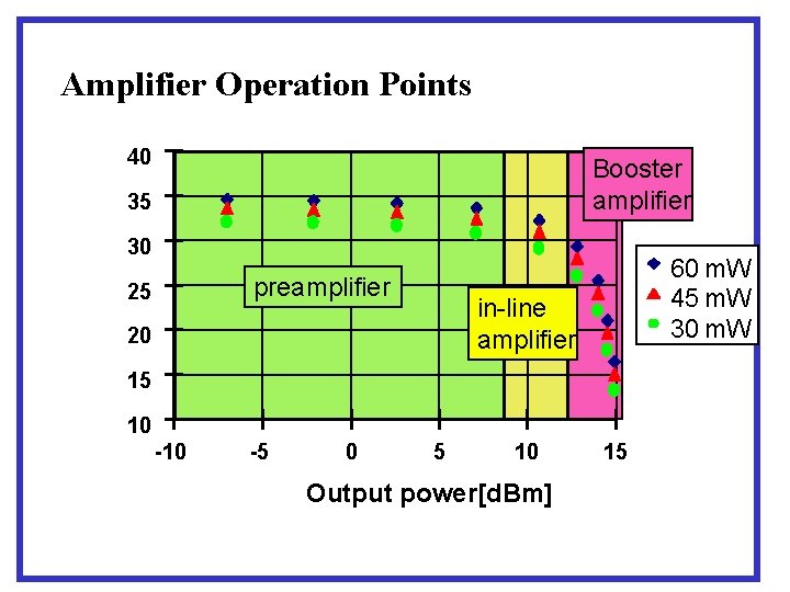
General Application of Optical Amplification • In-line amplifier: Able to amplify an attenuated signal so that it can travel an additional length of fiber, is called an optical line amplifier. • Preamplifier: is placed directly before the detector and may be integrated with it. • Power (booster) amplifier: it is placed right after the source, and thus may also be integrated with it. • LAN booster amplifier Amplifier Pump Lasers Standard Fiber

Amplifier Operation Points 40 Booster amplifier 35 30 preamplifier 25 60 m. W 45 m. W 30 m. W in-line amplifier 20 15 10 -5 0 5 10 Output power[d. Bm] 15

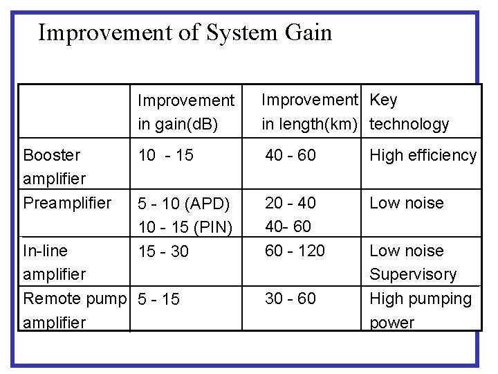
Improvement of System Gain Booster amplifier Preamplifier Improvement in gain(d. B) Improvement Key in length(km) technology 10 - 15 40 - 60 High efficiency 5 - 10 (APD) 10 - 15 (PIN) 15 - 30 20 - 40 40 - 60 60 - 120 Low noise In-line amplifier Remote pump 5 - 15 amplifier 30 - 60 Low noise Supervisory High pumping power

Erbium Doped Fiber Amplifiers (EDFA)

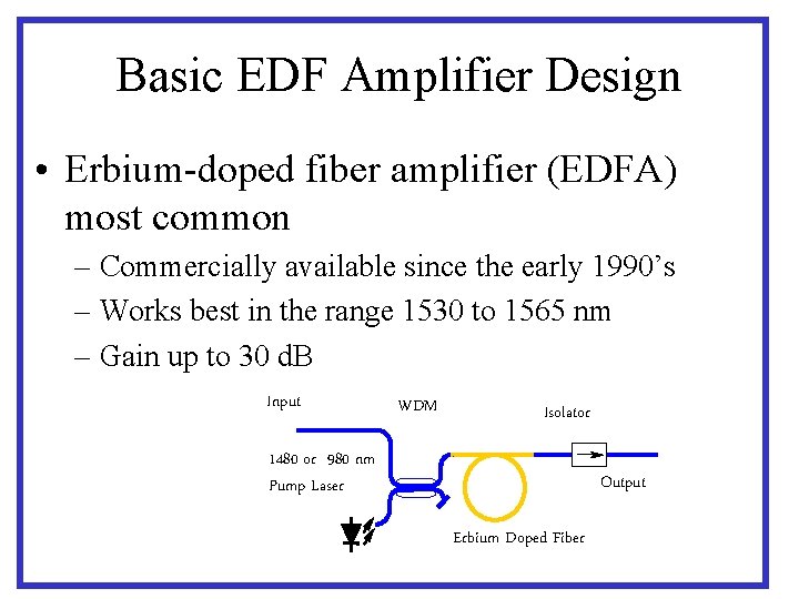
Basic EDF Amplifier Design • Erbium-doped fiber amplifier (EDFA) most common – Commercially available since the early 1990’s – Works best in the range 1530 to 1565 nm – Gain up to 30 d. B Input WDM Isolator 1480 or 980 nm Pump Laser Output Erbium Doped Fiber

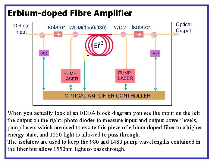
Erbium-doped Fibre Amplifier When you actually look at an EDFA block diagram you see the input on the left the output on the right, photo diodes to measure input and output power levels, pump lasers which are used to excite this piece of erbium doped fiber to a higher energy state, and 1550 light is allowed to pass through. The isolators are used to keep the 980 and 1480 pump wavelengths contained in the fiber but allow 1550 nm light to pass through.

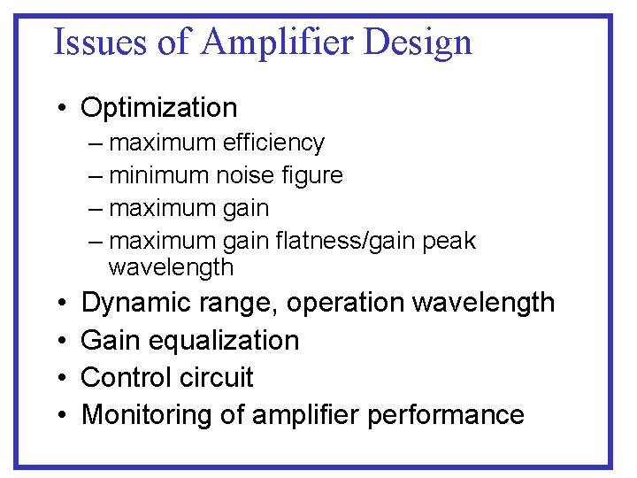
Issues of Amplifier Design • Optimization – maximum efficiency – minimum noise figure – maximum gain flatness/gain peak wavelength • • Dynamic range, operation wavelength Gain equalization Control circuit Monitoring of amplifier performance

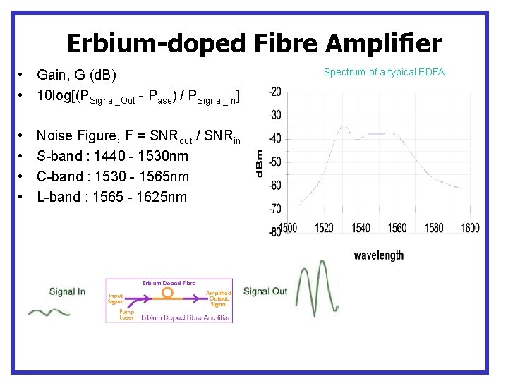
Erbium-doped Fibre Amplifier • Gain, G (d. B) • 10 log[(PSignal_Out - Pase) / PSignal_In] • • Noise Figure, F = SNRout / SNRin S-band : 1440 - 1530 nm C-band : 1530 - 1565 nm L-band : 1565 - 1625 nm Spectrum of a typical EDFA

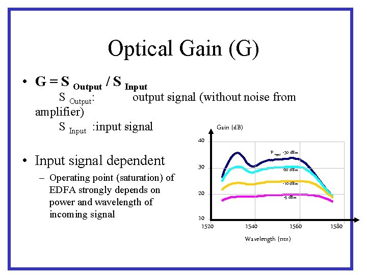
Optical Gain (G) • G = S Output / S Input S Output: output signal (without noise from amplifier) Gain (d. B) S Input : input signal 40 • Input signal dependent – Operating point (saturation) of EDFA strongly depends on power and wavelength of incoming signal P Input: -30 d. Bm 30 20 10 1520 -20 d. Bm -10 d. Bm -5 d. Bm 1540 1560 Wavelength (nm) 1580

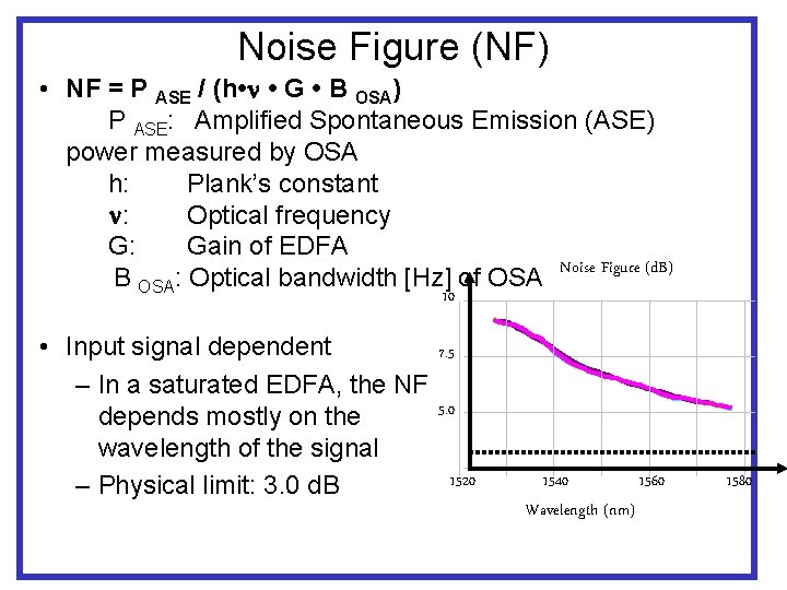
Noise Figure (NF) • NF = P ASE / (h • • G • B OSA) P ASE: Amplified Spontaneous Emission (ASE) power measured by OSA h: Plank’s constant : Optical frequency G: Gain of EDFA Noise Figure (d. B) B OSA: Optical bandwidth [Hz] of OSA 10 • Input signal dependent – In a saturated EDFA, the NF depends mostly on the wavelength of the signal – Physical limit: 3. 0 d. B 7. 5 5. 0 1520 1540 Wavelength (nm) 1560 1580

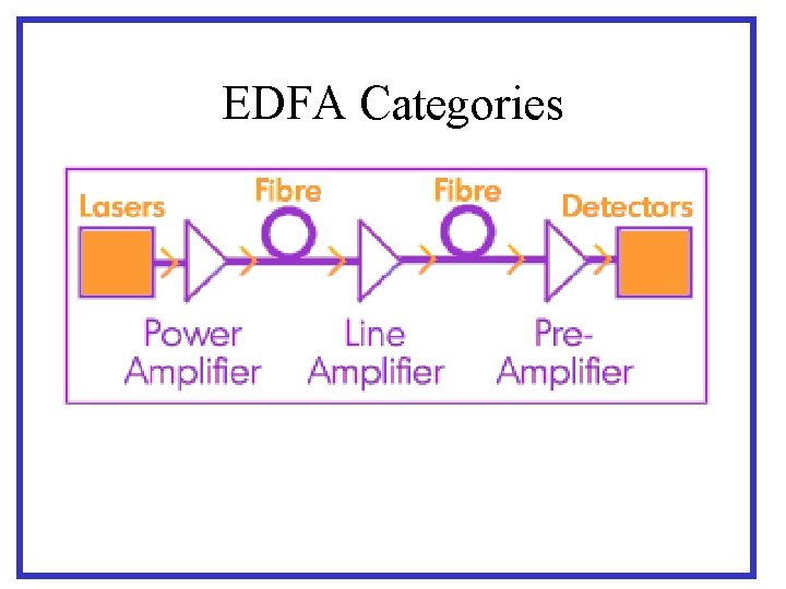
EDFA Categories • In-line amplifiers – Installed every 30 to 70 km along a link – Good noise figure, medium output power • Power boosters – Up to +17 d. Bm power, amplifies transmitter output – Also used in cable TV systems before a star coupler • Pre-amplifiers – Low noise amplifier in front of receiver • Bi-directional amplifiers – An amplifier which work in both ways

EDFA Categories

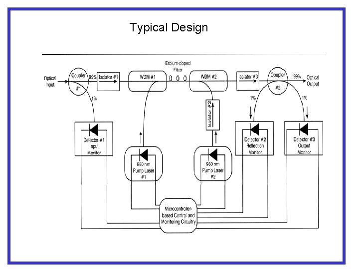
Typical Design • Figure in the slide shows an EDFA with all the options design – Coupler #1 is for monitoring input light – Coupler #2 is optional and is used for monitoring backreflections. The microcontroller can be set to disable the pump lasers in case the connector on the output has been disconnected. This provides a measure of safety for technicians working with EDFA’s.

Typical Design

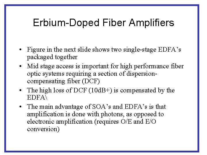
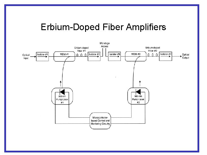
Erbium-Doped Fiber Amplifiers • Figure in the next slide shows two single-stage EDFA’s packaged together • Mid stage access is important for high performance fiber optic systems requiring a section of dispersioncompensating fiber (DCF) • The high loss of DCF (10 d. B+) is compensated by the EDFA • The main advantage of SOA’s and EDFA’s is that amplification is done with photons, as opposed to electronic amplification (requires O/E and E/O conversion)

Erbium-Doped Fiber Amplifiers

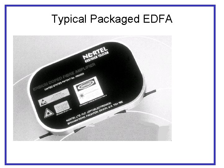
Typical Packaged EDFA

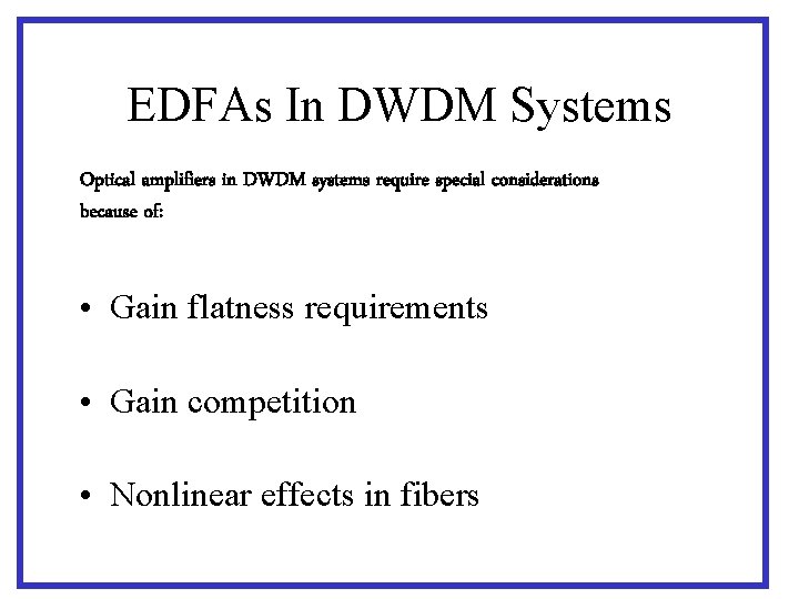
EDFAs In DWDM Systems Optical amplifiers in DWDM systems require special considerations because of: • Gain flatness requirements • Gain competition • Nonlinear effects in fibers

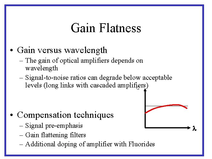
Gain Flatness • Gain versus wavelength – The gain of optical amplifiers depends on wavelength – Signal-to-noise ratios can degrade below acceptable levels (long links with cascaded amplifiers) G • Compensation techniques – Signal pre-emphasis – Gain flattening filters – Additional doping of amplifier with Fluorides

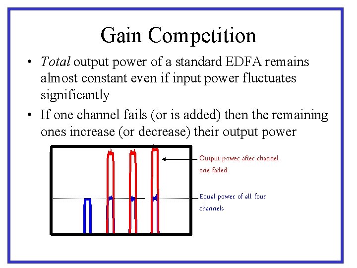
Gain Competition • Total output power of a standard EDFA remains almost constant even if input power fluctuates significantly • If one channel fails (or is added) then the remaining ones increase (or decrease) their output power Output power after channel one failed Equal power of all four channels

Output Power Limitations • High power densities in SM fiber can cause – – Stimulated Brillouin scattering (SBS) Stimulated Raman scattering (SRS) Four wave mixing (FWM) Self-phase and cross-phase modulation (SPM, CPM) • Most designs limit total output power to +17 d. Bm – Available channel power: 50/N m. W (N = number of channels)

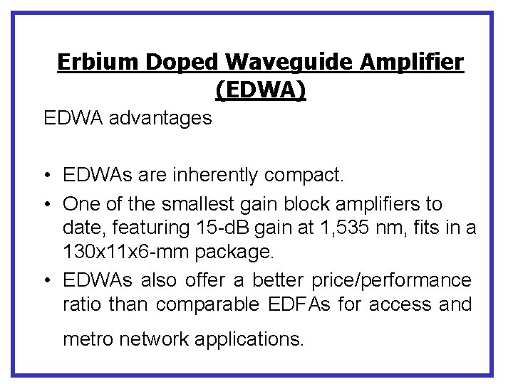
Erbium Doped Waveguide Amplifier (EDWA) • An erbium-doped waveguide amplifier (EDWA) consists of waveguides embedded in an amorphous erbium-doped glass substrate. • The erbium atoms provide the glass with gain in the 1, 550 -nm fibre-optic window. • The waveguide itself is a localised increase in the glass refractive index. • Today's manufacturers have several methods available to produce erbium-doped glass waveguides: PECVD and flame hydrolysis deposition, sputtering, ion-exchange, or ion implantation. • For the manufacture of waveguide amplifiers, the two most advanced methods are ion-exchange and sputtering.

Erbium Doped Waveguide Amplifier (EDWA) EDWA advantages • EDWAs are inherently compact. • One of the smallest gain block amplifiers to date, featuring 15 -d. B gain at 1, 535 nm, fits in a 130 x 11 x 6 -mm package. • EDWAs also offer a better price/performance ratio than comparable EDFAs for access and metro network applications.

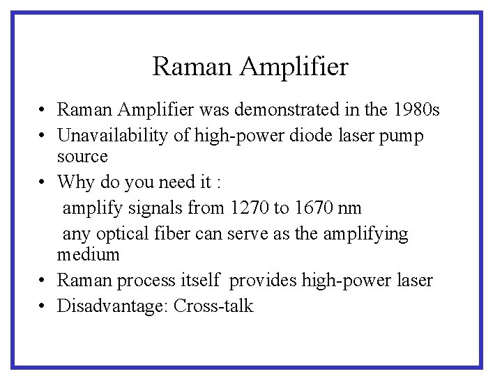
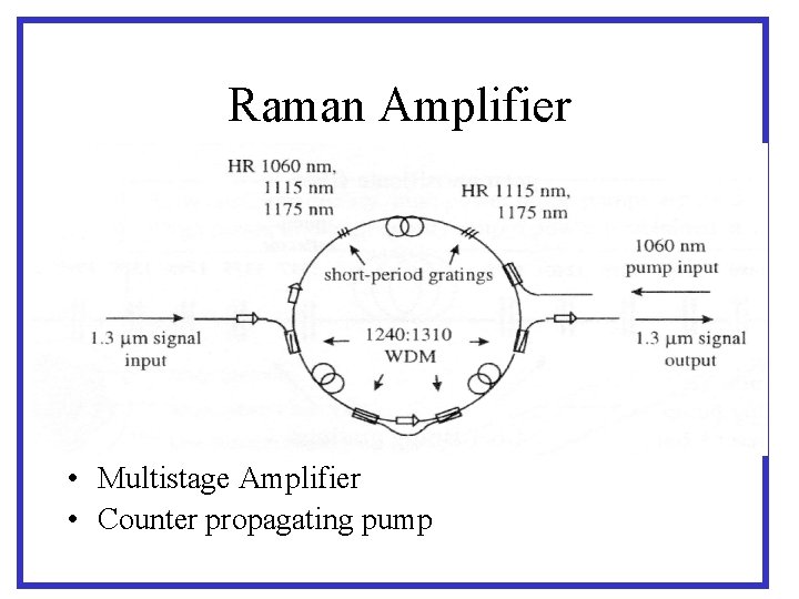
Raman Amplifier • Raman Amplifier was demonstrated in the 1980 s • Unavailability of high-power diode laser pump source • Why do you need it : amplify signals from 1270 to 1670 nm any optical fiber can serve as the amplifying medium • Raman process itself provides high-power laser • Disadvantage: Cross-talk

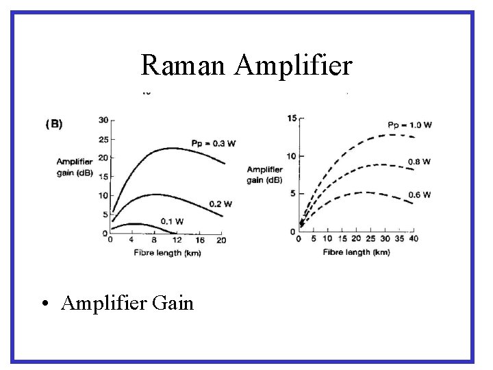
Raman Amplifier • Amplifier Gain

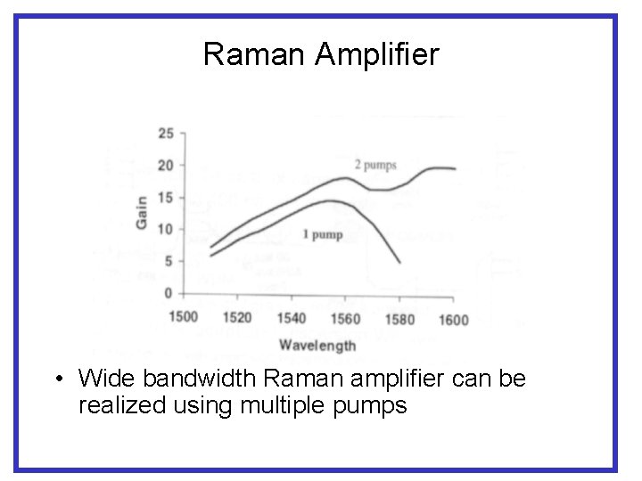
Raman Amplifier • Wide bandwidth Raman amplifier can be realized using multiple pumps

Raman Amplifier • Multistage Amplifier • Counter propagating pump

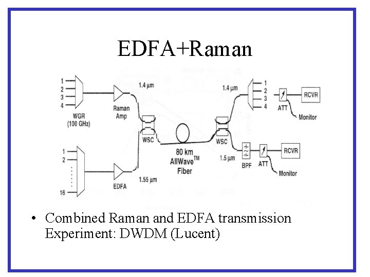
EDFA+Raman • Combined Raman and EDFA transmission Experiment: DWDM (Lucent)

Raman Amplifier • High-power laser sources are available by Raman process itself. • 200 to 400 nm Bandwidth Amplifiers are possible Raman, EDFA combination Flat gain for WDM New fiber lasers and gratings make it practical • System with Terabits of capacity are possible

Semiconductor Optical Amplifier (SOA) – Basically a laser chip without any mirrors – Metastable state has nanoseconds lifetime (-> nonlinearity and crosstalk problems) – Potential for switches and wavelength converters

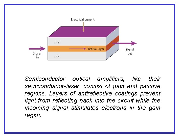
Semiconductor optical amplifiers, like their semiconductor-laser, consist of gain and passive regions. Layers of antireflective coatings prevent light from reflecting back into the circuit while the incoming signal stimulates electrons in the gain region

Semiconductor Optical Amplifier (SOA) • Semiconductor optical amplifiers are similar in construction to semiconductor lasers. They consist of a gain (active) section and a passive section constructed of a semiconductor material such as indium phosphide. The main difference is that SOAs are made with layers of antireflection coatings to prevent light from reflecting back into the circuit. Optical gain occurs as excited electrons in the semiconductor material are stimulated by incoming light signals; when current is applied across the p-n junction the process causes the photons to replicate, producing signal gain. The gain medium can be either a bulk or a multiple-quantum-well active layer.

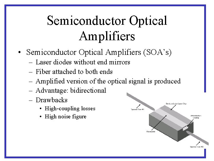
Semiconductor Optical Amplifiers • Semiconductor Optical Amplifiers (SOA’s) – – – Laser diodes without end mirrors Fiber attached to both ends Amplified version of the optical signal is produced Advantage: bidirectional Drawbacks • High-coupling losses • High noise figure

Semiconductor • By adjusting the chemical composition of III-V semiconductors (typically Ga. In. As. P) the band gap can be adjusted to give optical gain in the telecommunications windows of interest. The devices are typically 250 mm long although devices of up to 1 mm have been made. In general the longer devices can achieve higher gain and wider bandwidths. • The optical bandwidth of a semiconductor optical amplifier (SOA) can be as large as 100 nm and the fact that the energy source is a DC electrical current makes these devices look promising as optical amplifiers.

Semiconductor • • • There are two aspects of their properties which has prevented their widescale deployment. The SOA is fundamentally nonlinear as the device refractive index and the device gain depend on the amount of population inversion. Since this inversion changes as the signal is amplified this leads to amplitude and phase changes being applied to the signal. The short lifetimes of the device (100 ps-1 ns) also make these effects apparent at the single pulse level and as a pattern dependent effect. The second problem is that the noise performance of these devices is inferior to the Erbium fibre amplifier. One final drawback is that the usual geometry of the semiconductor waveguide is rectangular and the silica waveguide is circular. This leads to a mismatch of the fundamental mode patterns and the typical loss in going from one to the other is 3 d. B. Even so fibre to fibre gains of over 20 d. B can be achieved.

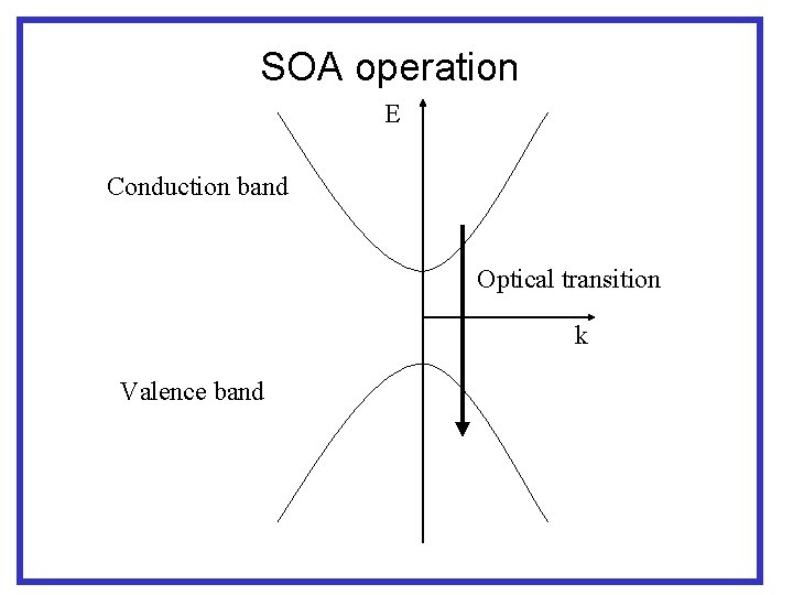
SOA operation E Conduction band Optical transition k Valence band

SOA operation • The DC current applied to the device results in electrons being pumped into the (normally empty) conduction band removed from the (normally full) valence band. This creates the population inversion which is a pre-cursor to optical gain. When signal photons travel through the device they cause stimulated emission to occur when an electron and hole recombine. • The phase effects in these devices can be quite strong with a gain change of 3 d. B corresponding to roughly a phase change of p.