CMOS AMPLIFIERS Simple Inverting Amplifier Differential Amplifiers Cascode


 = 0, y(s) satisfies: These dynamics are the characteristic dynamics of the")


 When w ∞, A(s)")

")


2")


")


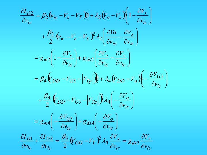


 KCL at D 1: KCL at D 2:")
 = gm 1 / (gds 2 +")


=AV(s/z 1 -1)(s/z 2 -1)/(s/p 1 -1)(s/p")

 § GBW should be at least")


… M 4")


DVo ÞDVGS 2= ro 1(gm")

- Slides: 87
CMOS AMPLIFIERS • • • Simple Inverting Amplifier Differential Amplifiers Cascode Amplifier Output Amplifiers Summary
Simple Inverting Amplifiers
Inverter with diode connection load Small Signal Characteristics How do you get better matching?
High gain inverters
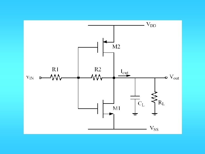
Current source load or push-pull • Refer to book for large signal analysis • Must match quiescent currents in PMOS and NMOS transistors • Wider output swing, especially push-pull • Much high gain (at DC), but much lower 3 d. B frequency (vs diode load) • About the same GB • Very power dependent
Small signal High gain!
Key to analysis by hand: • Use level 1 or 3 model equations • Use KCL/KVL
Dependence of Gain upon Bias Current
Transfer function of a system input u System output y
When u(s) = 0, y(s) satisfies: These dynamics are the characteristic dynamics of the system. The roots of the coefficient polynomial are the poles of the system. When y(s) = 0, u(s) satisfies: These dynamics are the zero dynamics of the system. The roots of the coefficient polynomial are the zeros of the system.
Frequency Response of CMOS Inverters
Poles of CMOS Inverters Let vin = 0, x = 0, VDD = 0, VSS = 0. y CGS 1, CGS 2, CBS 1, CBS 2 are all short CGD 1, CGD 2, CBD 1, CBD 2, CL in parallel C’L = Ctotal = CGD 1+ CGD 2+ CBD 1+ CBD 2+ CL
Total conductance from y to ground: go = gds 1 + gds 2 KCL at node y: Therefore system pole is:
Zeros of CMOS Inverters Let vin = x = u, VDD = 0, VSS = 0. CGD 1, CGD 2, are in parallel, CBD 1, CBD 2, CL are all short gds 1, gds 2 also short No current in them KCL: Zero is:
Input output transfer function When s=jw 0, A(0) When w ∞, A(s)
A 0=gm/go Acl=1/b 0 d. B |p 1|= g 0/CL’ Unity gain frequency =|A 0 p 1| =GB =gm/CL’ -3 d. B frequency of closed loop =b*GB |z 1| =gm/Cgd =GB*CL’/Cgd
Unity gain feedback A(s)
If a step input is given, the output response is In the time domain: Final settling determined by A 0 need high gain Settling speed determined by A 0 p 1=GB, need high gain bandwidth product
Gain bandwidth product C’L = Ctotal = CGD 1+ CGD 2+ CBD 1+ CBD 2+ CL When CL ≈ C’L, W↑ GB↑, but it saturates, when
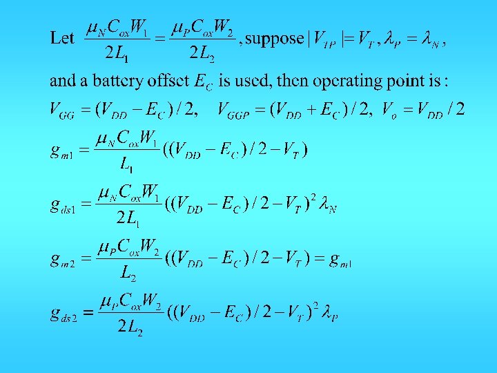
Note: If VEB 1 and VEB 2 are fixed, W 1/L 1 and W 2/L 2 must be adjusted proportionally, and they are proportional to DC power.
Therefore: P is proportional to W 1, W 2 CL constant, but C(W 1, W 2) proportional to W 1, W 2 When C(W 1, W 2) << CL, GB proportional to P When C(W 1, W 2) CL or >CL, GB saturates
GB Linear increase region P
NOISE IN MOS INVERTERS
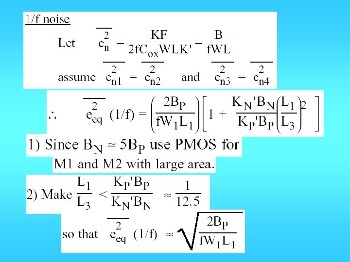
For 1/f noise:
For thermal noise
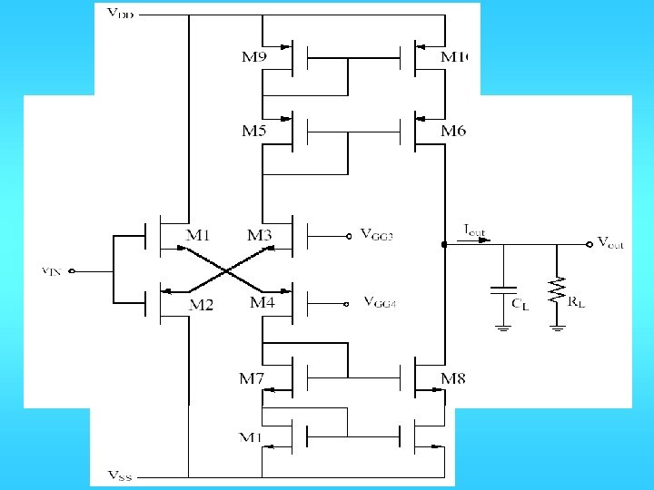
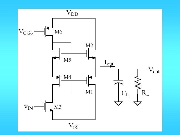
Noise in Push-Pull current source load Inverter
Differential Input, single-ended output single stage Amplifier N-Channel vin+ vin-
P-channel
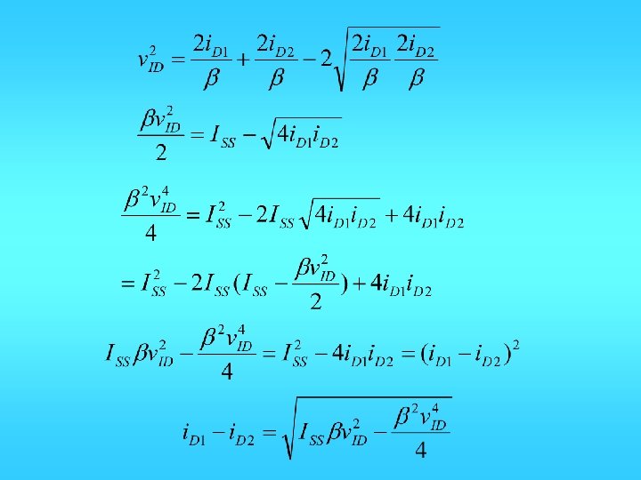
Large Signal Eq. in a N-channel Differential pair =0. 5 b 1(VGS 1 -VT)2 =(2 ID 1/b 1)0. 5 i. D 1=0, when i. D 2=ISS and VGS 2=VT+(2 ISS/b)0. 5
Solving for i. D 1 and i. D 2 i. D 1=i. D 2=ISS/2 VON 1=VON 2=(ISS/b)0. 5
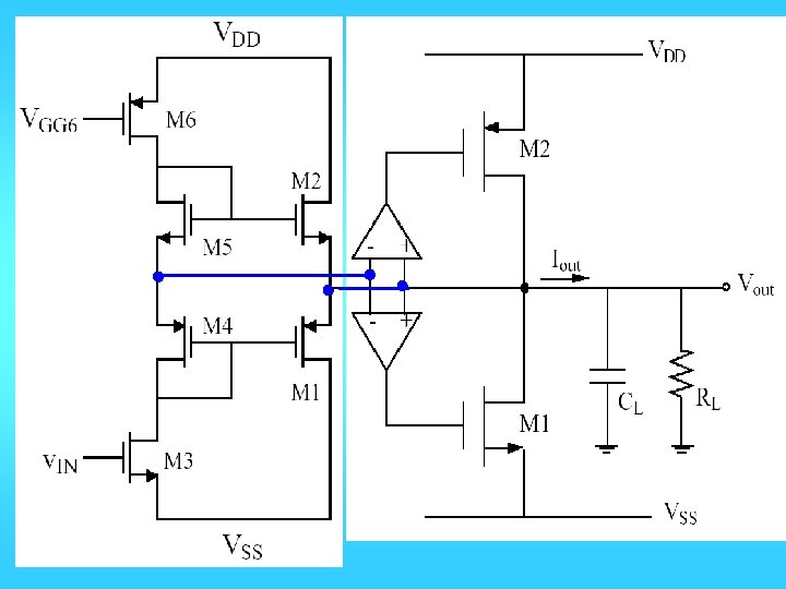
N-Channel Input Pair Differential Amplifier C. M. Load Simple current reference C. M. Bias
Voltage transfer curve
P-Channel Input Pair Differential Amplifier
Voltage transfer curve
INPUT COMMON MODE RANGE VG 1=VG 2=Vi. CM VSDSAT 1=VSDSAT 2 =VON VD 1=VD 3= VSS+VT 3+VON VG 1 min=VD 1 -|VT 1| VG 1 max=VDDVSD 5 SAT-|VT 1|-VON
Output Range Vomin=Vss+Von 4 Vomax=Vicm –|VT 2| So what’s the vo range What’s for the N-ch circuit.
SMALL SIGNAL ANALYSIS AV
Common Mode Equivalent Circuit, with perfect match i. C 1=VIC/(1/gm 1 +2 rds 5) ro 1≈1/gm 3 i. C 1 ACM≈ 1/ 2 rds 5 gm 3 CMRR=Av/ACM=2 gm 1 gm 3/(gds 4+gds 2)/gds 5
If not perfectly matched io=ai. IC a is a fraction go 1≈ gds 2 + gds 4 i. C 1 ACM≈ agds 5 / 2(gds 2 + gds 4) CMRR=Av/ACM=2 gm 1/agds 5
Formal detailed analysis
SLEW RATE: the limit of the rate of change of the output voltage C’Ldvo/dt=i 4 -i 2 ISS Max |CLdvo/dt|=ISS Slew Rate = ISS/C’L ISS 0 Output swing: Vosw GB frequency: f. GB vo(t)=Voswsin(2 pf. GBt) Max dvo/dt =Vosw 2 pf. GB To avoid slewing: ISS > C’L Vosw 2 pf. GB
Parasitic Capacitances CT: common mode only CM: mirror cap = Cdg 1 + Cdb 1 + Cgs 3 + Cgs 4 + Cdb 3 COUT = output cap = Cbd 4 + Cbd 2 + Cgd 2 + CL
• Impedances – rout = rsd 2 || rds 4 = 1 / (gds 2 + gds 4) – r. M = 1/gm 3 || rds 1 ≈ 1/ gm 3 – Hence the output node is the high impedance node • When vi=0, slowest discharging node is output node with dominant pole p 1 = -1/(C’outrout), where C’out = Cout+ Cgd 4 • Approximate transfer function AV(s) = AV/(s/p 1─1)
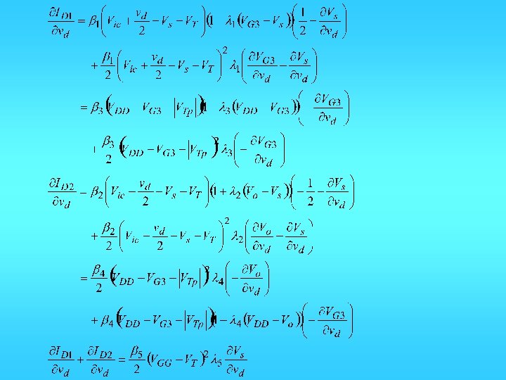
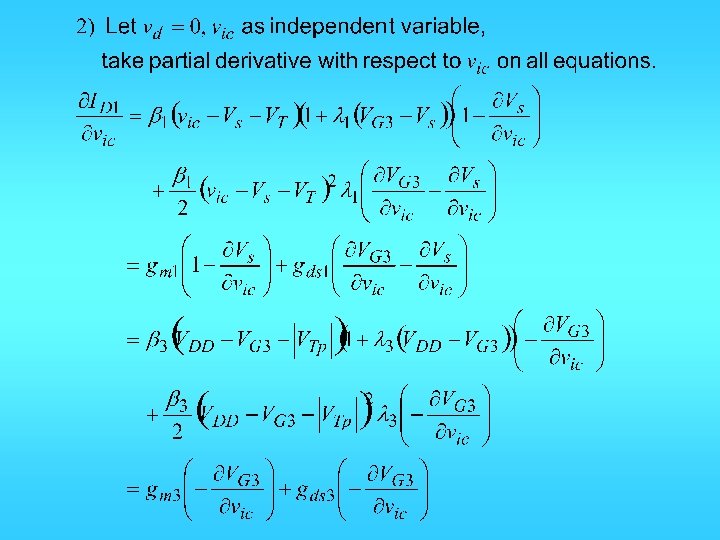
When v. G 1=v. G 2=0(AC) KCL at D 1: KCL at D 2:
Gain bandwidth product • • Gain AV(0) = gm 1 / (gds 2 + gds 4) Bandwidth ≈ |p 1| ≈ (gds 2 + gds 4) / C’out GBW ≈ gm 1 / C’out gm 1 = {2*ID 1 m. Cox. W 1/L 1}½ – increase gm 1 increase GBW – increase W 1 increase GBW • But C’out has Cdb 2 and Cgd 2 W 1 – Once Cdb 2 and Cgd 2 become comparable to CL, increasing W 1 reduces GBW
Other poles and zeros VDD Second pole at D 1 M 4 r = 1/gm 3 Cgd 4 C = CM + M 3 (1+AV 4)Cgd 4 Vi+ M 1 Vb 2 M 5 VOUT Cgd 4 (1+AV 4)Cgd 4 CL AV 4 = gm 4/gds 4 Vi- p 2 = ─ gm 3 CM + (1+AV 4)Cgd 4
VDD M 3 Unstable zero at Cgd 2 Enforce vo=0, float vin. M 4 ids 2, ids 4 = 0 VOUT CL Vi+ = - Vi- M 1 Vb 2 M 5 Vi- Cgd 2 dvi-/dt = gm 2 viz 1 = gm 2/Cgd 2
VDD For zero at D 1: M 3 For diff, Vi+ = - Viwhich is set by Cgd 2 M 4 VOUT CL Vi+ M 1 M 2 Vi- z 2 = Vb 2 M 5 Both Cgd 4 and Cgd 1 to gnd Ctot = CM + Cgd 4 ─gm 3 CM + Cgd 4
• A better approximation of TF: AV(s)=AV(s/z 1 -1)(s/z 2 -1)/(s/p 1 -1)(s/p 2 -1) • If p 1 is dominant, |p 1|<<|p 2|, |z 1|, |z 2|; AV(s)≈AV/(s/p 1 -1) • If p 1 is non-dominant, at low frequency, AV(s)≈AV /(s/p 1+s/p 2 -s/z 1 -s/z 2 -1) • 1/peq≈ 1/p 1+1/p 2 -1/z 1 -1/z 2 ≈ 1/p 1+1/p 2 -1/z 2 , since |z 1| >> |z 2|, |p 1|, |p 2|; ≈ 1/p 1, if AV 4 is not very large • In either case, BW ≈ p 1
frequency response AV All in abs val z 1 p 2 z 2 UGF -90 -180 PM w
Observations • PM ≈ 90 – tan-1(UGF/z 1) § GBW should be at least 2~3 times lower than z 1 to ensure good phase margin at UGF § There is conflict between AV and PM • If z 2 not = p 2, UGF < AV*p 1 • Design approaches • make z 1 higher than UGF • make Cgd 2 small, gm 1 large • make z 2 close to p 2 better 1 st order approx. • make AV 4 small • make p 1 low large AV • make gds 2 and gds 4 small
Design Steps • Select Iss based on – GB & V_osw, SR, or P_max • Select W 1/L 1 based on – GB = gm/CL’, Assuming CL’ = (1. 1~1. 5)CL – Maximize z 1 (minimize Cgd 2) • Select W 4/L 4 based on – ICMR, – Small Av 4 • Select W 5/L 5 based on – ICMR
NOISE Model
Input equivalent noise source
• Total output noise current is found as, • Let • Then
How does this affect Av 4 and go?
Cascoding • Objectives – Increase ro – Increase AV – Remove feed forward from vin to vo – Remove unstable zero • Methods – Direct cascoding – Folded cascoding
CMOS CASCODE AMPLIFIERS VDD Rb Rb Vin CL M 1 Vbb Vin M 2 M 1 Vout-min increase by VON 2 Vout-max decreased if a Cascoded source used Output swing is a big CL Problem in low voltage Applications
Cascoded current source load VDD Vyy Vxx Vbb Vin M 4 M 3 M 2 M 1 Q: How should you set the bias? Q: what is Vout-max? ro = AV = CL ro at D 1? v. D 1 = vin
VDD Vyy Vxx Vbb Vin High frequency model AV 0(s/z 1 -1)… M 4 AV(s) = M 3 Consider only the effect of the lower half circuit. M 2 M 1 CL (s/p 1 -1)(s/p 2 -1)… For poles, short input, and compute the time constants at each node. For zeros, float input but require vo = 0. (don’t short vo!)
VDD Vyy Vxx Vbb Vin Short vin, float vo: At the high impedance node M 3 r =rds 1(gm 2+gmb 2)rds 2 C =CL+Cdb 2+Cgd 2 p 1 = -1/RC M 2 At the low impedance CL node M 4 M 1 r =1/(gm 2+gmb 2+gds 1+gds 2) C =Cgd 1+Cdb 1+Cgs 2+Csb 2 p 2 =
VDD Vyy Vxx Vbb Vin M 4 M 3 M 2 vs 2=0 Enforce vo=0, float vin. i. Co=0, no current cross line, and i. Cgd 2=0 id 2, id 3 = 0, gm 2 vgs 2=0 At the G 1 -D node CL igds 1=0 s. Cgd 1 vin=gm 1 vin M 1 Was the unstable zero removed?
Gain bandwidth product • If |p 1| << |p 2|, |p 3|, …, |p 1| << |z 1|, |z 2|, … – BW ≈ |p 1| – GBW ≈ gm 1/Co • Otherwise – AV(s) ≈ AV/(s/p 1+s/p 2…-s/z 1 -s/z 2… - 1) – 1/BW ≈ 1/p 1+2/p 2…-1/z 1 -2/z 2… = RC 1 + RC 2 + …
Any enhancement? Note: rds 2, Rb 1/ID 2 VDD gm 2 √ID 2 Effects on: Rb Vbb Vin ro, AV M 2 M 1 CL Co, GBW Slew rate
Another possible modification VDD Rb Effects on: ro, AV? Co, GBW? Vbb Vin M 2 CL Slew rate? M 1 poles? zeros?
Folded cascoding Which I source should be cascoded? VDD ro, AV? M 1 Vin M 1 Vbb CL Co, GBW? Slew rate? poles? zeros?
OUTPUT AMPLIFIERS • Requirements – Provide sufficient output power in the form of voltage or current. – Avoid signal distortion for large signal swings. – Be power efficient. – Provide protection from abnormal conditions. • Types of Output Stages – Class A amplifier. – Source follower. – Push-Pull amplifier ( inverting and follower). – Negative feedback (OP amp and resistive).
Power efficiency • It is most power efficient at maximum signal level • Let VSS= ─VDD, Vin is sinusoidal such that Vout reaches Voutmax • PRL = ½ (Voutmax)2/RL • Psupply=average((VDD or VSS)*IRL) =VDD*average(Voutmax/RL *sin()) =2*VDD*Voutmax/RL/p • Power efficicy = PRL/Psupply<p/4 (78%)
CLASS A AMPLIFIER ro, AV, z, p as before Power effic = PRL Psupply 0. 5 voutmax. IQ = I (V -V ) < 25% Q DD SS VSS=-VDD, Voutmax=VDD-Vdssat
SOURCE FOLLOWER or VSS+VT
Push-pull
Push-pull inverting amp
Implementation
PUSH-PULL SOURCE FOLLOWER
Negative Feedback To Reduce Rout Ro=?
Super source follower DVo => DI 1 =(gm 1+gmb 1)DVo ÞDVGS 2= ro 1(gm 1+gmb 1)DVo ÞDI 2 = gm 2 ro 1(gm 1+gmb 1)DVo VDD I 1 Vo M 1 Vin M 2 I 2 go=gm 2 ro 1(gm 1+gmb 1) +(gm 1+gmb 1)+go 2 ≈gm 2 ro 1(gm 1+gmb 1) Gm ≈gm 1+gm 1 ro 1 gm 2 gm 1 AV=Gm/go≈ g + g m 1 mb 1 Ex: rework these when I 1 and I 2 have finite ros.
VDD If we re-arrange with a flipped version, we get this push-pull super source follower I 1 M 4 M 2 Vo M 1 Vin M 3 I 2 Ex: provide a transistor level implementation. Comment on power efficiency.