
5 CMOS Logic Basics1combinational logic Contents 1 Dynamic
5 CMOS Logic Basics(1)-combinational logic Contents 1. Dynamic NMOS logic 2. Pseudo NMOS logic l Transistor sizing l Complex logic gate layout 3. Static(complementary) CMOS logic l Inverter, NAND, NOR gates layout 4. Pass transistor logic 5. Bi. CMOS logic 6. Dynamic CMOS logic 1
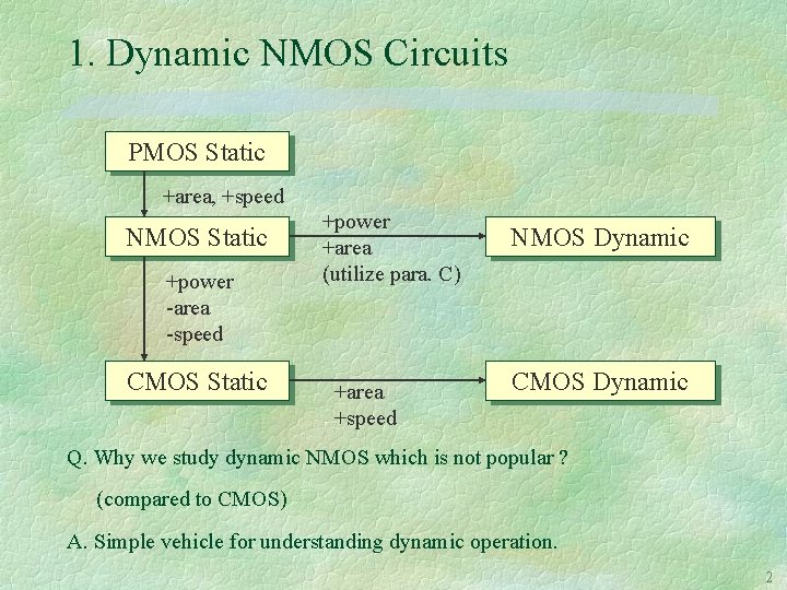
1. Dynamic NMOS Circuits PMOS Static +area, +speed NMOS Static +power -area -speed CMOS Static +power +area (utilize para. C) +area +speed NMOS Dynamic CMOS Dynamic Q. Why we study dynamic NMOS which is not popular ? (compared to CMOS) A. Simple vehicle for understanding dynamic operation. 2
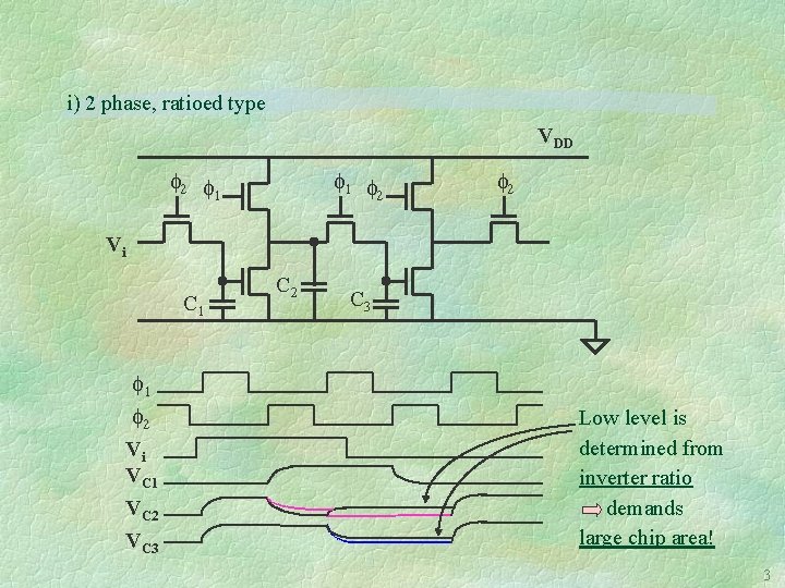
i) 2 phase, ratioed type VDD 2 1 1 2 2 Vi C 1 1 2 Vi VC 1 VC 2 VC 3 C 2 C 3 Low level is determined from inverter ratio demands large chip area! 3
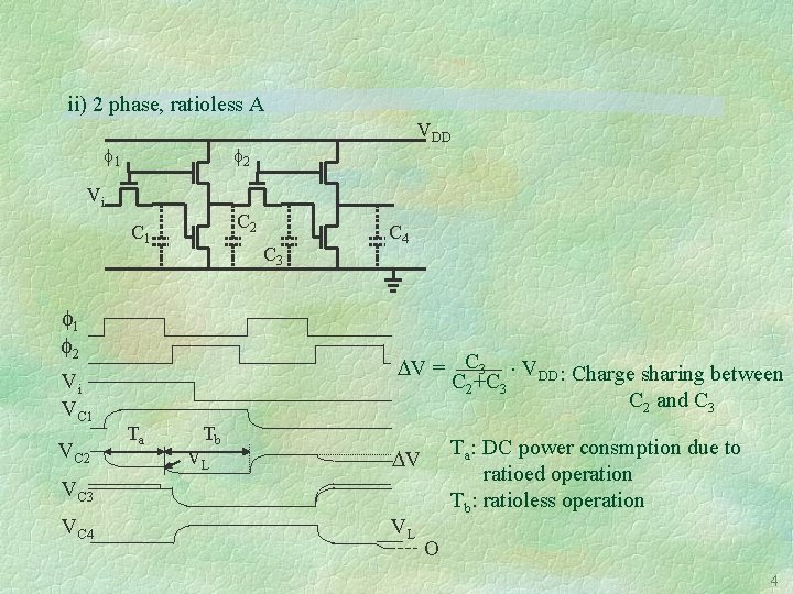
ii) 2 phase, ratioless A 1 VDD 2 Vi C 2 C 1 C 3 1 2 Vi VC 1 VC 2 C 4 DV = C 3 VDD : Charge sharing between C 2+C 3 C 2 and C 3 Ta Tb VL Ta: DC power consmption due to ratioed operation Tb: ratioless operation DV VC 3 VC 4 VL O 4
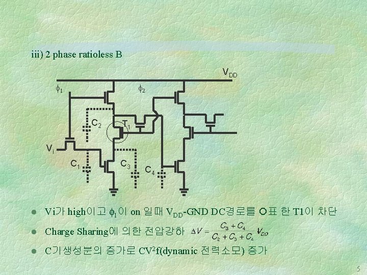
iii) 2 phase ratioless B VDD 1 2 C 2 T 1 Vi C 1 C 3 C 4 l Vi가 high이고 1이 on 일때 VDD-GND DC경로를 표 한 T 1이 차단 l Charge Sharing에 의한 전압강하 l C기생성분의 증가로 CV 2 f(dynamic 전력소모) 증가 5
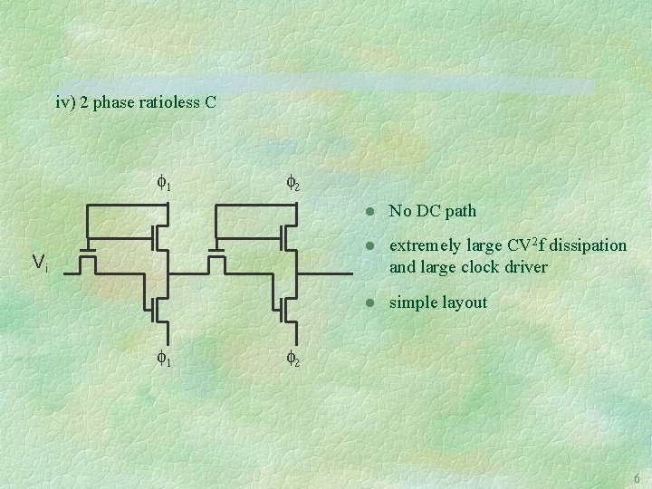
iv) 2 phase ratioless C 1 2 Vi 1 l No DC path l extremely large CV 2 f dissipation and large clock driver l simple layout 2 6
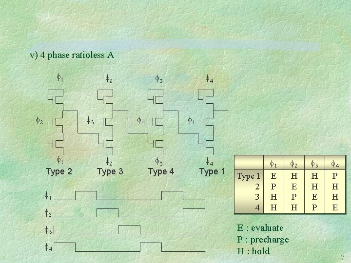
v) 4 phase ratioless A 1 2 2 3 1 Type 2 1 2 3 4 3 4 2 Type 3 4 1 3 Type 4 4 Type 1 2 3 4 1 2 3 4 E P H H H E P P H H E E : evaluate P : precharge H : hold 7
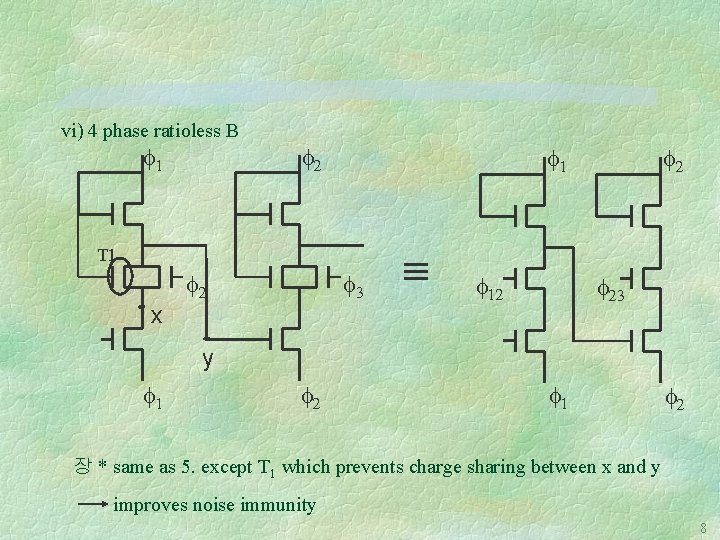
vi) 4 phase ratioless B 1 2 T 1 x 2 3 12 23 y 1 2 장 * same as 5. except T 1 which prevents charge sharing between x and y improves noise immunity 8
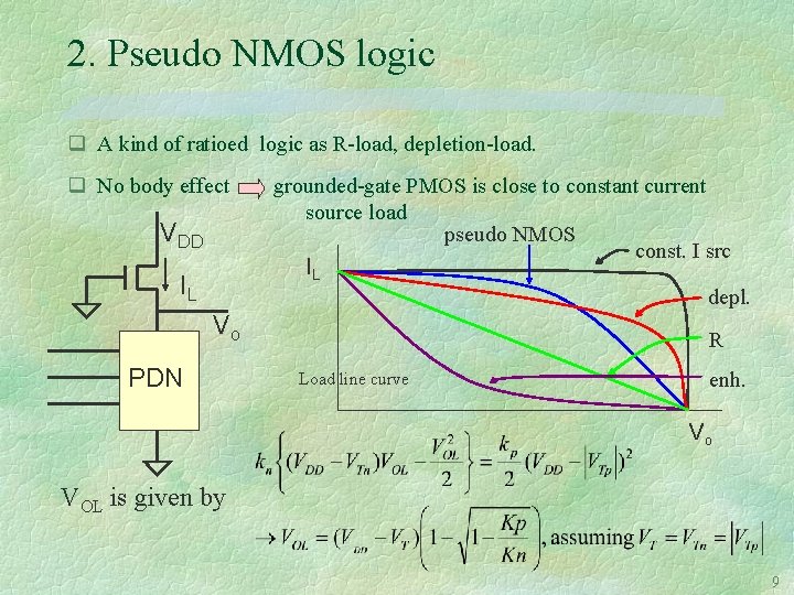
2. Pseudo NMOS logic q A kind of ratioed logic as R-load, depletion-load. q No body effect VDD IL grounded-gate PMOS is close to constant current source load pseudo NMOS const. I src IL depl. Vo PDN R Load line curve enh. Vo VOL is given by 9
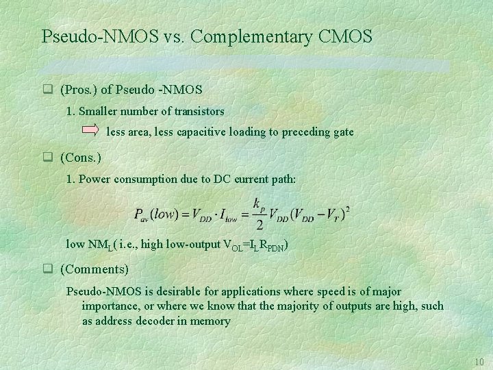
Pseudo-NMOS vs. Complementary CMOS q (Pros. ) of Pseudo -NMOS 1. Smaller number of transistors less area, less capacitive loading to preceding gate q (Cons. ) 1. Power consumption due to DC current path: low NML( i. e. , high low-output VOL=ILRPDN) q (Comments) Pseudo-NMOS is desirable for applications where speed is of major importance, or where we know that the majority of outputs are high, such as address decoder in memory 10
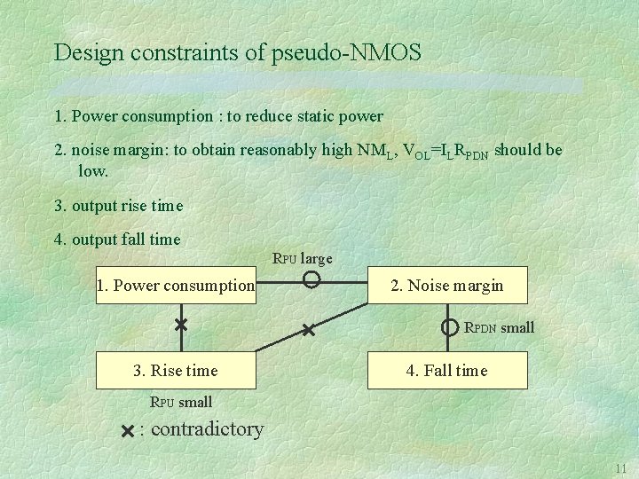
Design constraints of pseudo-NMOS 1. Power consumption : to reduce static power 2. noise margin: to obtain reasonably high NML, VOL=ILRPDN should be low. 3. output rise time 4. output fall time RPU large 1. Power consumption 2. Noise margin RPDN small 3. Rise time 4. Fall time RPU small : contradictory 11
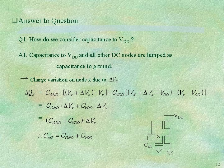
q. Answer to Question Q 1. How do we consider capacitance to VDD ? A 1. Capacitance to VDD and all other DC nodes are lumped as capacitance to ground. Charge variation on node x due to = = VDD = x Ceff 12
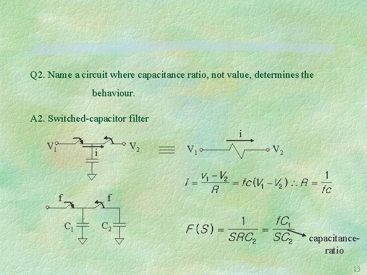
Q 2. Name a circuit where capacitance ratio, not value, determines the behaviour. A 2. Switched-capacitor filter i V 1 V 2 i f V 1 V 2 f C 1 C 2 capacitanceratio 13
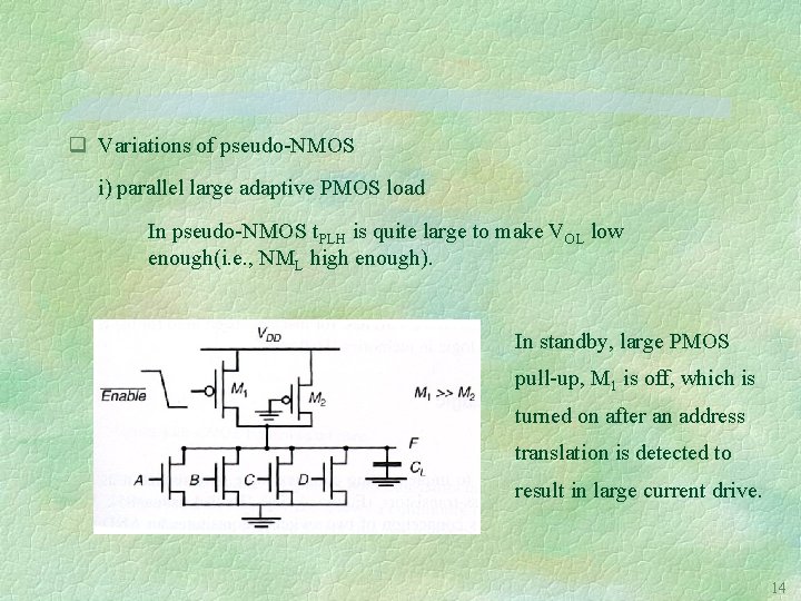
q Variations of pseudo-NMOS i) parallel large adaptive PMOS load In pseudo-NMOS t. PLH is quite large to make VOL low enough(i. e. , NML high enough). In standby, large PMOS pull-up, M 1 is off, which is turned on after an address translation is detected to result in large current drive. 14
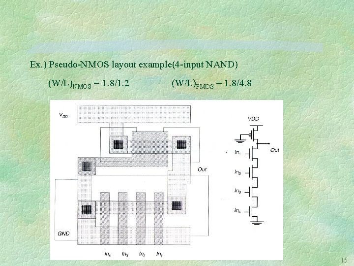
Ex. ) Pseudo-NMOS layout example(4 -input NAND) (W/L)NMOS = 1. 8/1. 2 (W/L)PMOS = 1. 8/4. 8 15
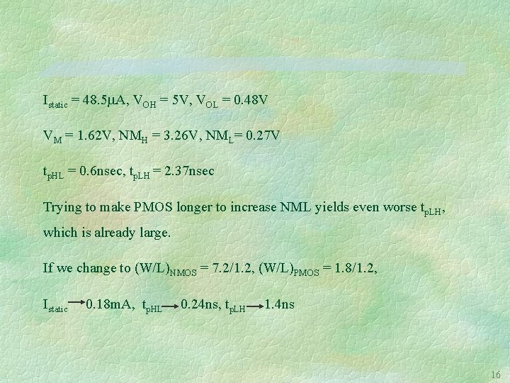
Istatic = 48. 5 A, VOH = 5 V, VOL = 0. 48 V VM = 1. 62 V, NMH = 3. 26 V, NML= 0. 27 V tp. HL = 0. 6 nsec, tp. LH = 2. 37 nsec Trying to make PMOS longer to increase NML yields even worse tp. LH, which is already large. If we change to (W/L)NMOS = 7. 2/1. 2, (W/L)PMOS = 1. 8/1. 2, Istatic 0. 18 m. A, tp. HL 0. 24 ns, tp. LH 1. 4 ns 16
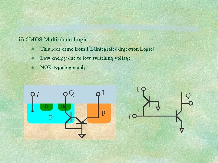
ii) CMOS Multi-drain Logic l This idea came from I 2 L(Integrated-Injection Logic). l Low energy due to low switching voltage l NOR-type logic only Q i n n p I I p Q i 17
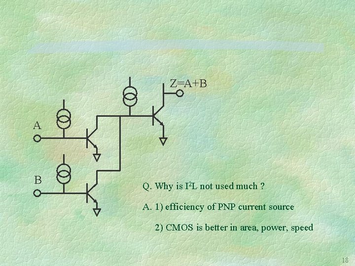
Z=A+B A B Q. Why is I 2 L not used much ? A. 1) efficiency of PNP current source 2) CMOS is better in area, power, speed 18
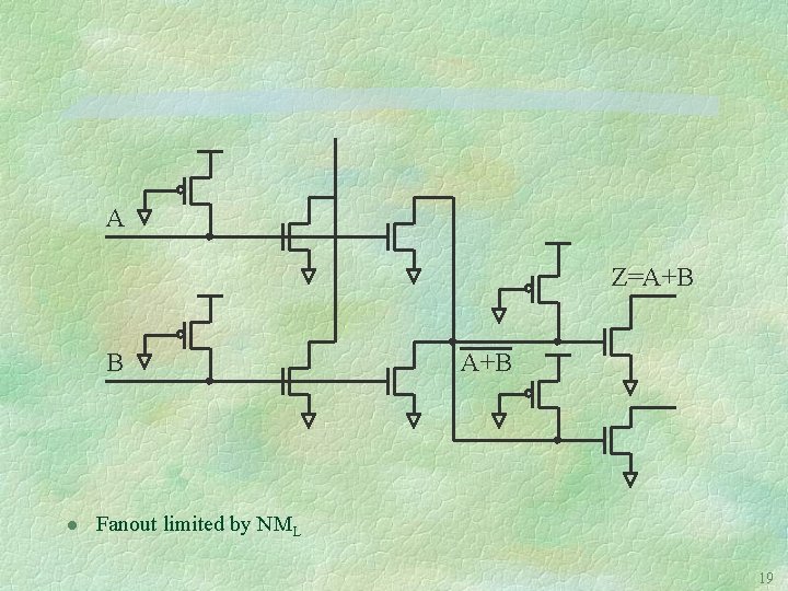
A Z=A+B B l A+B Fanout limited by NML 19
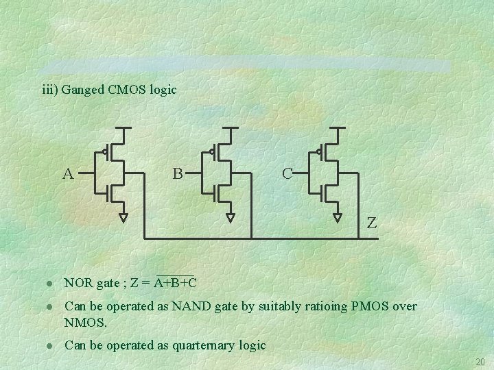
iii) Ganged CMOS logic A B C Z l NOR gate ; Z = A+B+C l Can be operated as NAND gate by suitably ratioing PMOS over NMOS. l Can be operated as quarternary logic 20
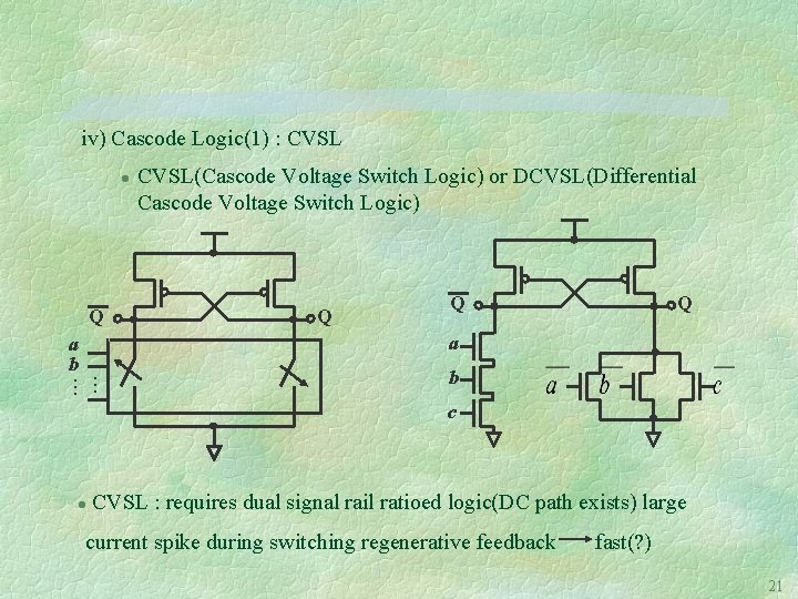
iv) Cascode Logic(1) : CVSL l Q CVSL(Cascode Voltage Switch Logic) or DCVSL(Differential Cascode Voltage Switch Logic) Q Q Q a a b . . . b c l CVSL : requires dual signal rail ratioed logic(DC path exists) large current spike during switching regenerative feedback fast(? ) 21
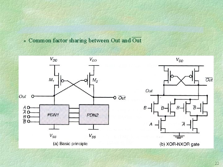
l Common factor sharing between Out and Out 22
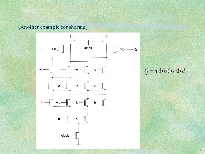
(Another example for sharing) 23
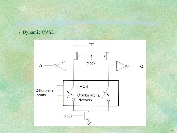
l Dynamic CVSL 24
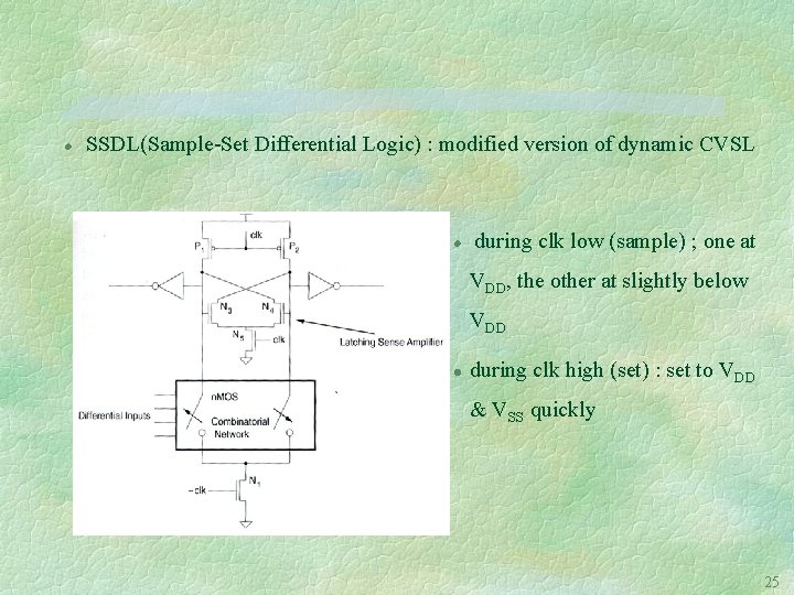
l SSDL(Sample-Set Differential Logic) : modified version of dynamic CVSL l during clk low (sample) ; one at VDD, the other at slightly below VDD l during clk high (set) : set to VDD & VSS quickly 25
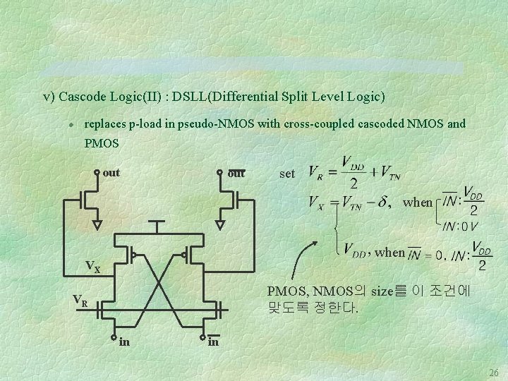
v) Cascode Logic(II) : DSLL(Differential Split Level Logic) l replaces p-load in pseudo-NMOS with cross-coupled cascoded NMOS and PMOS out set when VX PMOS, NMOS의 size를 이 조건에 맞도록 정한다. VR in in 26
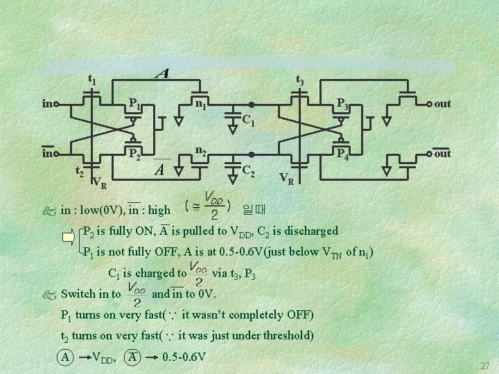
t 1 t 3 P 1 in n 1 P 3 out P 4 out C 1 in n 2 P 2 t 2 C 2 VR k in : low(0 V), in : high VR 일때 P 2 is fully ON, A is pulled to VDD, C 2 is discharged P 1 is not fully OFF, A is at 0. 5 -0. 6 V(just below VTN of n 1) C 1 is charged to k Switch in to via t 3, P 3 and in to 0 V. P 1 turns on very fast( it wasn’t completely OFF) t 2 turns on very fast( it was just under threshold) A VDD, A 0. 5 -0. 6 V 27
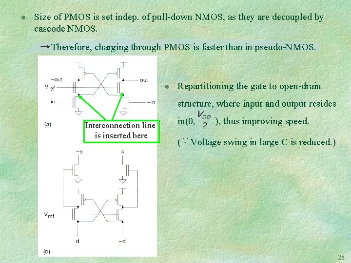
Size of PMOS is set indep. of pull-down NMOS, as they are decoupled by cascode NMOS. Therefore, charging through PMOS is faster than in pseudo-NMOS. l Repartitioning the gate to open-drain structure, where input and output resides Interconnection line is inserted here in(0, ), thus improving speed. l ( Voltage swing in large C is reduced. ) 28
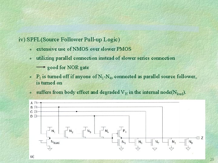
iv) SPFL(Source Follower Pull-up Logic) l extensive use of NMOS over slower PMOS l utilizing parallel connection instead of slower series connection good for NOR gate l l P 1 is turned off if anyone of N 1 -N 4, connected as parallel source follower, is turned on suffers from body effect and degraded VH in the internal node(Nload). 29
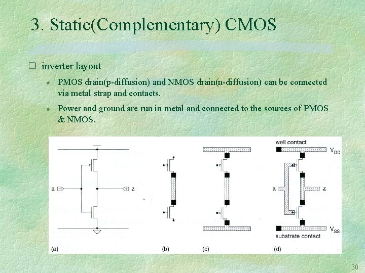
3. Static(Complementary) CMOS q inverter layout l l PMOS drain(p-diffusion) and NMOS drain(n-diffusion) can be connected via metal strap and contacts. Power and ground are run in metal and connected to the sources of PMOS & NMOS. 30
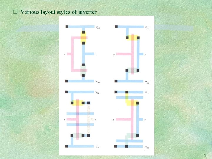
q Various layout styles of inverter 31
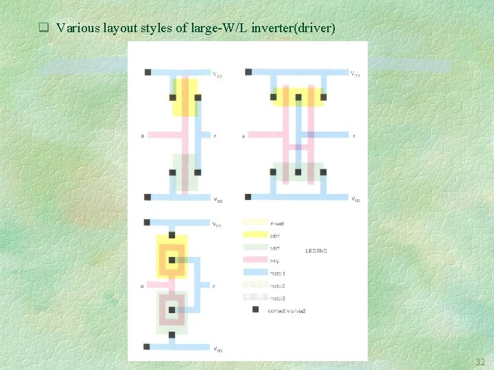
q Various layout styles of large-W/L inverter(driver) 32
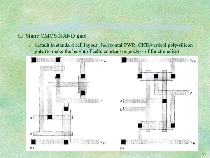
q Static CMOS NAND gate l default in standard cell layout : horizontal PWR, GND/vertical poly-silicon gate (to make the height of cells constant regardless of functionality) 33
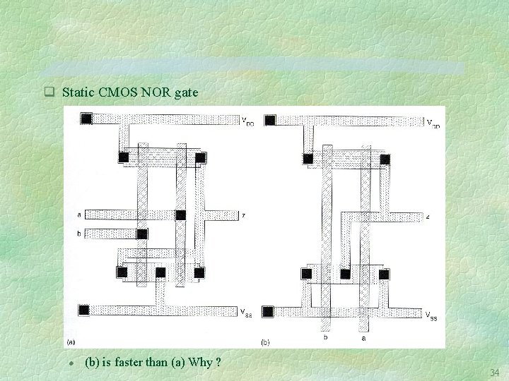
q Static CMOS NOR gate l (b) is faster than (a) Why ? 34
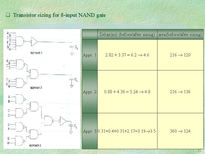
q Transistor sizing for 8 -input NAND gate Delay(ns) (before/after sizing) area(before/after sizing) Appr. 1 2. 82 + 3. 37 = 6. 2 4. 6 216 120 Appr. 2 0. 88 + 4. 36 = 5. 24 4. 8 216 136 Appr. 3 0. 31+0. 4+0. 31+2. 17=3. 19 3. 5 360 124 35
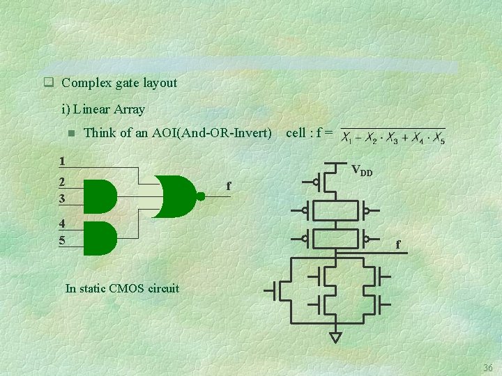
q Complex gate layout i) Linear Array n Think of an AOI(And-OR-Invert) 1 cell : f = VDD 2 3 f 4 5 f In static CMOS circuit 36
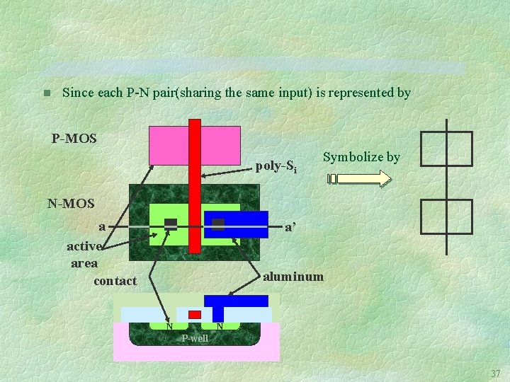
n Since each P-N pair(sharing the same input) is represented by P-MOS poly-Si Symbolize by N-MOS a active area contact a’ aluminum N N P-well 37
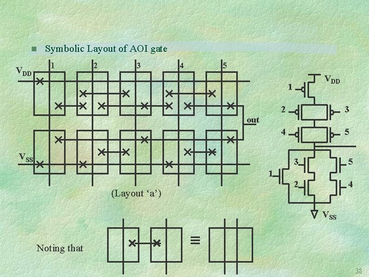
n VDD Symbolic Layout of AOI gate 1 2 3 4 5 VDD 1 2 3 4 5 out VSS 3 5 2 4 1 (Layout ‘a’) VSS Noting that 38
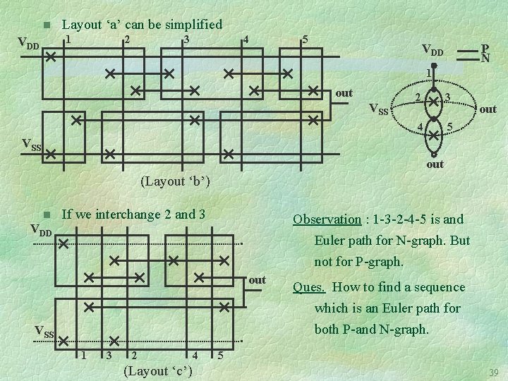
n Layout ‘a’ can be simplified 1 VDD 2 3 4 5 VDD P N 1 out VSS 2 3 4 5 out VSS out (Layout ‘b’) n If we interchange 2 and 3 Observation : 1 -3 -2 -4 -5 is and Euler path for N-graph. But not for P-graph. VDD out VSS 1 3 2 (Layout ‘c’) 4 Ques. How to find a sequence which is an Euler path for both P-and N-graph. 5 39
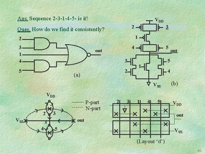
Ans. Sequence 2 -3 -1 -4 -5 - is it! VDD 2 Ques. How do we find it consistently? 3 1 2 3 1 4 4 out 3 5 2 (a) 5 out 5 1 4 VSS (b) VDD 2 VSS 3 2 3 1 4 5 VDD out 1 4 P-part N-part 5 VSS (Layout ‘d’) 40
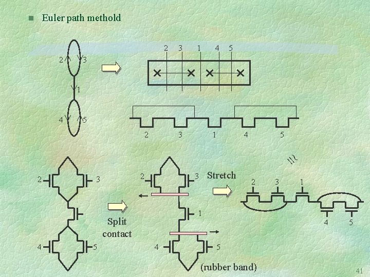
Euler path methold n 2 2 3 1 4 5 2 2 3 5 2 3 1 1 Split contact 4 Stretch 3 4 4 5 5 (rubber band) 41
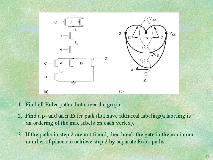
1. Find all Euler paths that cover the graph. 2. Find a p- and an n-Euler path that have identical labeling(a labeling is an ordering of the gate labels on each vertex). 3. If the paths in step 2 are not found, then break the gate in the minimum number of places to achieve step 2 by separate Euler paths. 42
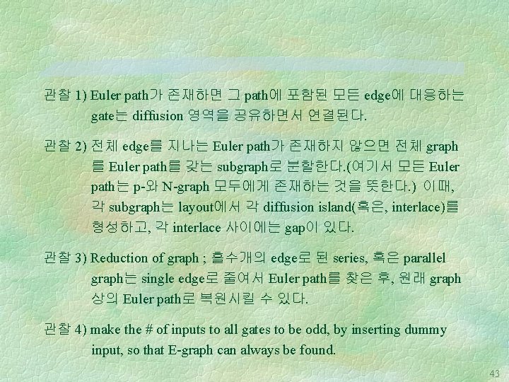
관찰 1) Euler path가 존재하면 그 path에 포함된 모든 edge에 대응하는 gate는 diffusion 영역을 공유하면서 연결된다. 관찰 2) 전체 edge를 지나는 Euler path가 존재하지 않으면 전체 graph 를 Euler path를 갖는 subgraph로 분할한다. (여기서 모든 Euler path는 p-와 N-graph 모두에게 존재하는 것을 뜻한다. ) 이때, 각 subgraph는 layout에서 각 diffusion island(혹은, interlace)를 형성하고, 각 interlace 사이에는 gap이 있다. 관찰 3) Reduction of graph ; 홀수개의 edge로 된 series, 혹은 parallel graph는 single edge로 줄여서 Euler path를 찾은 후, 원래 graph 상의 Euler path로 복원시킬 수 있다. 관찰 4) make the # of inputs to all gates to be odd, by inserting dummy input, so that E-graph can always be found. 43
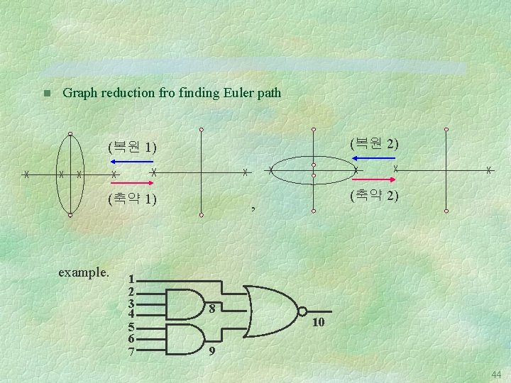
n Graph reduction fro finding Euler path (복원 2) (복원 1) (축약 1) example. 1 2 3 4 5 6 7 (축약 2) , 8 10 9 44
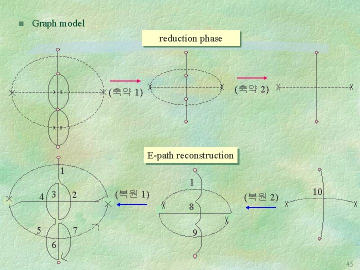
n Graph model reduction phase (축약 2) (축약 1) E-path reconstruction 1 1 4 3 2 5 7 (복원 1) 8 (복원 2) 10 9 6 45
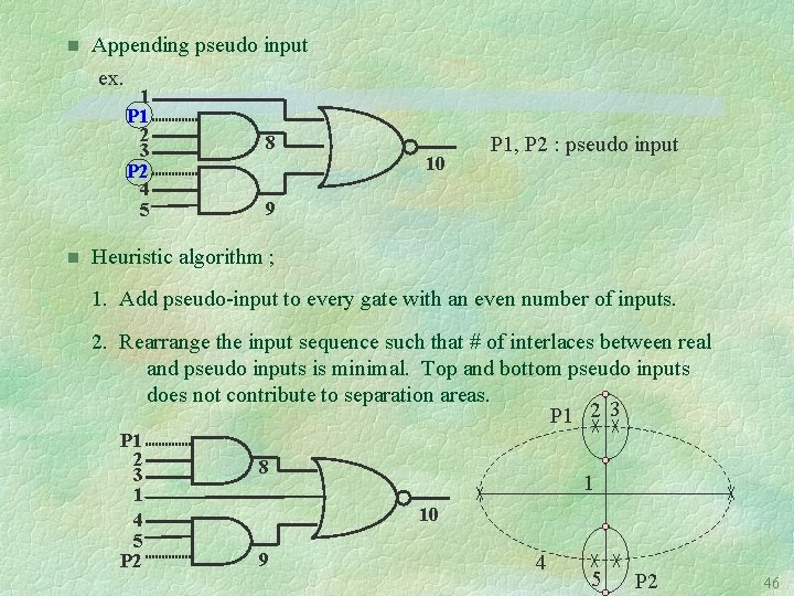
n Appending pseudo input ex. 1 P 1 2 3 P 2 4 5 n 8 10 P 1, P 2 : pseudo input 9 Heuristic algorithm ; 1. Add pseudo-input to every gate with an even number of inputs. 2. Rearrange the input sequence such that # of interlaces between real and pseudo inputs is minimal. Top and bottom pseudo inputs does not contribute to separation areas. P 1 2 3 1 4 5 P 2 8 1 10 9 4 5 P 2 46
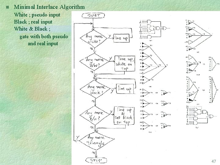
n Minimal Interlace Algorithm White ; pseudo input Black ; real input White & Black ; gate with both pseudo and real input 47
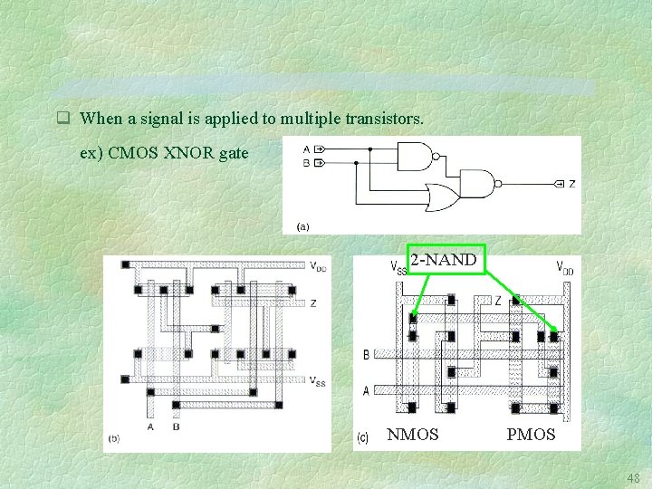
q When a signal is applied to multiple transistors. ex) CMOS XNOR gate 2 -NAND NMOS PMOS 48
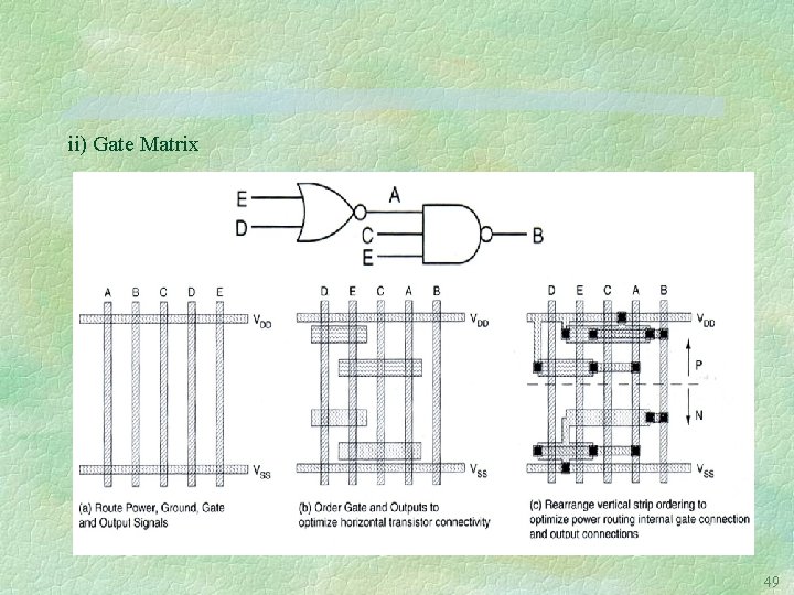
ii) Gate Matrix 49
q Gate Matrix layout algorithm l Transistors are grouped in strips to allow maximum source/drain connection by abutment. To achieve better grouping, polysilicon columns are allowed to interchange to increase abutment. l The resultant groups are then placed in rows with groups maximally connected to the VSS and VDD rails placed toward these signals. Row placement is then based on the density of other connections. l Routing is achieved by vertical diffusion or Manhattan(horizontal and vertical) metal routing. This normally would require a maze router. 50
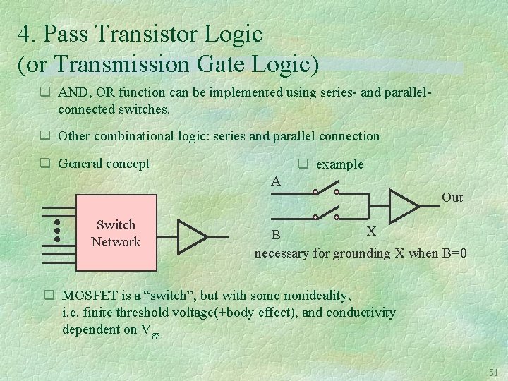
4. Pass Transistor Logic (or Transmission Gate Logic) q AND, OR function can be implemented using series- and parallelconnected switches. q Other combinational logic: series and parallel connection q General concept q example A Out Switch Network X B necessary for grounding X when B=0 q MOSFET is a “switch”, but with some nonideality, i. e. finite threshold voltage(+body effect), and conductivity dependent on Vgs 51
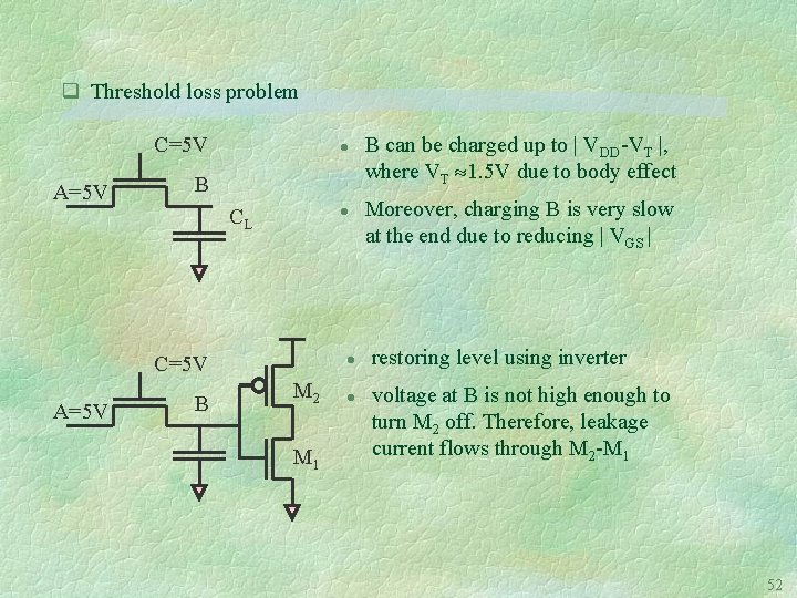
q Threshold loss problem C=5 V A=5 V l B CL l C=5 V A=5 V B l M 2 M 1 l B can be charged up to | VDD-VT |, where VT 1. 5 V due to body effect Moreover, charging B is very slow at the end due to reducing | VGS | restoring level using inverter voltage at B is not high enough to turn M 2 off. Therefore, leakage current flows through M 2 -M 1 52
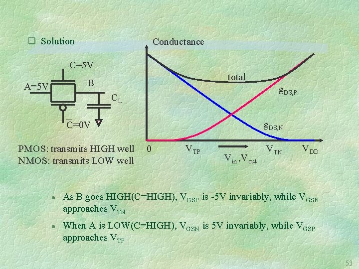
q Solution Conductance C=5 V total B A=5 V g. DS, P CL g. DS, N C=0 V PMOS: transmits HIGH well NMOS: transmits LOW well l l 0 VTP Vin , Vout VTN VDD As B goes HIGH(C=HIGH), VGSP is -5 V invariably, while VGSN approaches VTN When A is LOW(C=HIGH), VGSN is 5 V invariably, while VGSP approaches VTP 53
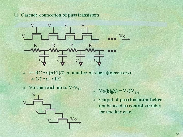
q Cascade connection of pass transistors V V Vo V R R C l l R C C = RC • n(n+1)/2, n: number of stages(transistors) 1/2 • n 2 • RC Vo can reach up to V-VTN V l l V Vo(high) = V-3 VTN Output of pass transistor better not be used as control variable for another gate. Vo 54
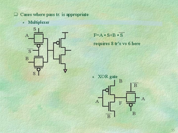
q Cases where pass tr. is appropriate l Multiplexer S F=A • S+B • S A requires 8 tr’s vs 6 here S B S l XOR gate A B B A F B B 55
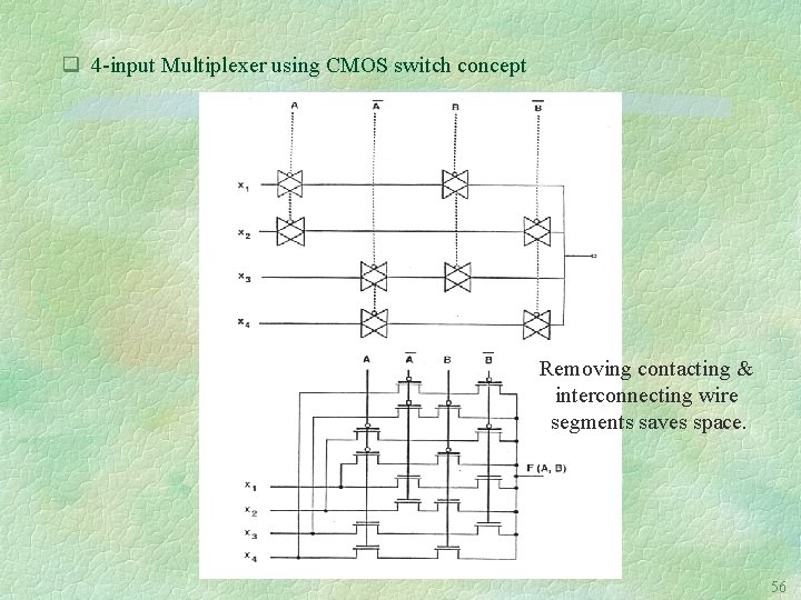
q 4 -input Multiplexer using CMOS switch concept Removing contacting & interconnecting wire segments saves space. 56
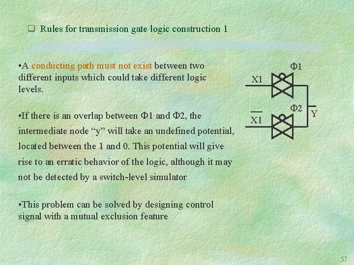
q Rules for transmission gate logic construction 1 • A conducting path must not exist between two different inputs which could take different logic levels. • If there is an overlap between 1 and 2, the 1 X 1 2 X 1 Y intermediate node “y” will take an undefined potential, located between the 1 and 0. This potential will give rise to an erratic behavior of the logic, although it may not be detected by a switch-level simulator • This problem can be solved by designing control signal with a mutual exclusion feature 57
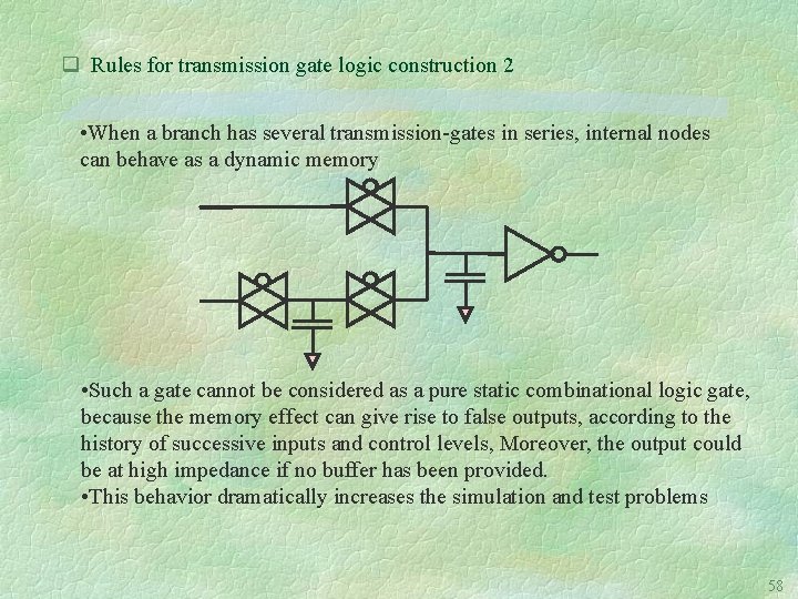
q Rules for transmission gate logic construction 2 • When a branch has several transmission-gates in series, internal nodes can behave as a dynamic memory • Such a gate cannot be considered as a pure static combinational logic gate, because the memory effect can give rise to false outputs, according to the history of successive inputs and control levels, Moreover, the output could be at high impedance if no buffer has been provided. • This behavior dramatically increases the simulation and test problems 58
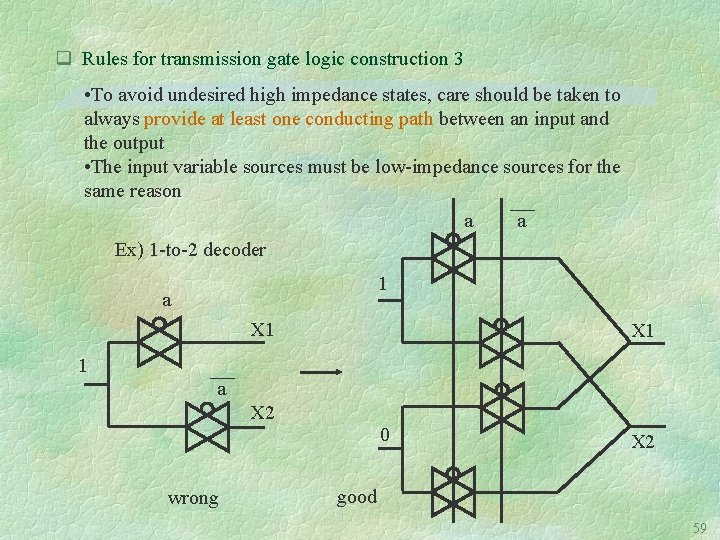
q Rules for transmission gate logic construction 3 • To avoid undesired high impedance states, care should be taken to always provide at least one conducting path between an input and the output • The input variable sources must be low-impedance sources for the same reason a a Ex) 1 -to-2 decoder 1 a X 1 1 a X 2 wrong 0 X 2 good 59
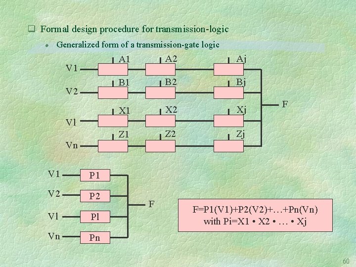
q Formal design procedure for transmission-logic l Generalized form of a transmission-gate logic V 1 V 2 A 1 A 2 Aj B 1 B 2 Bj X 1 X 2 Xj Z 1 Z 2 Zj F Vl Vn V 1 P 1 V 2 P 2 Vl Pl Vn Pn F F=P 1(V 1)+P 2(V 2)+…+Pn(Vn) with Pi=X 1 • X 2 • … • Xj 60
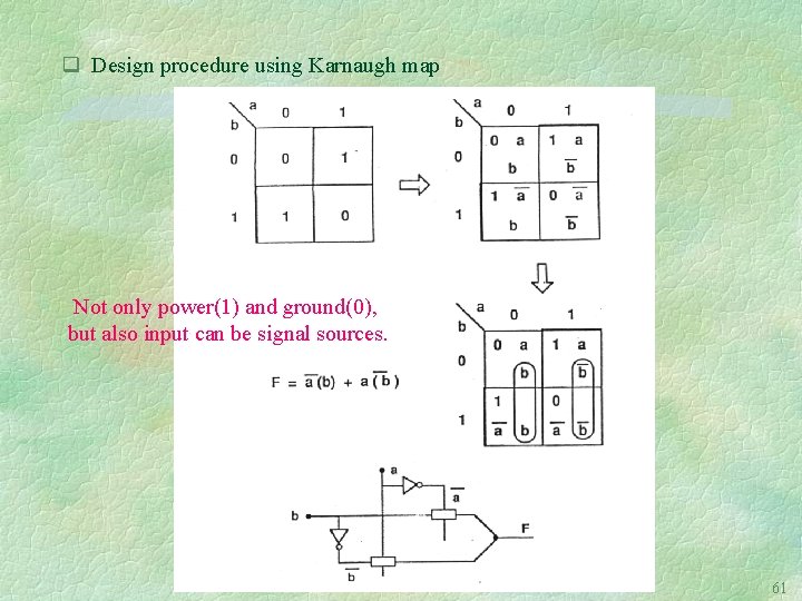
q Design procedure using Karnaugh map Not only power(1) and ground(0), but also input can be signal sources. 61
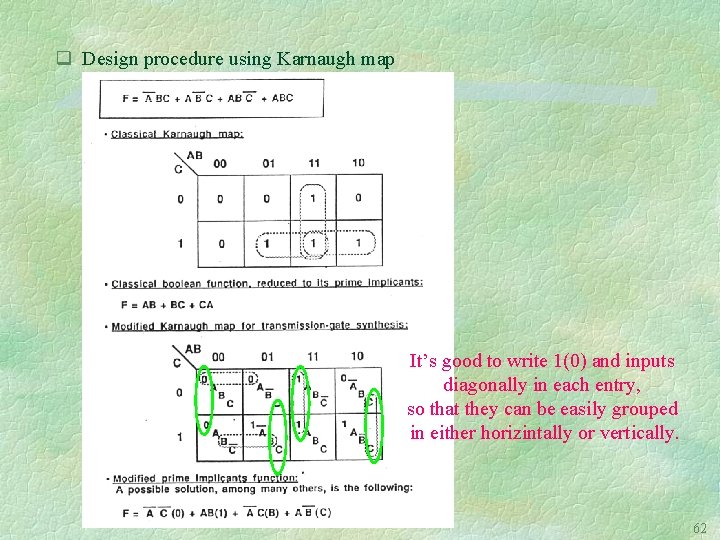
q Design procedure using Karnaugh map It’s good to write 1(0) and inputs diagonally in each entry, so that they can be easily grouped in either horizintally or vertically. 62
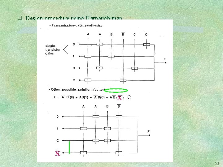
q Design procedure using Karnaugh map x c x 63
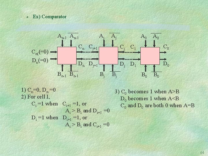
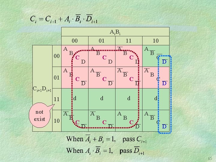
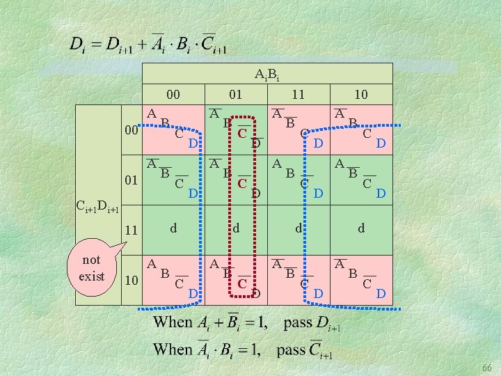
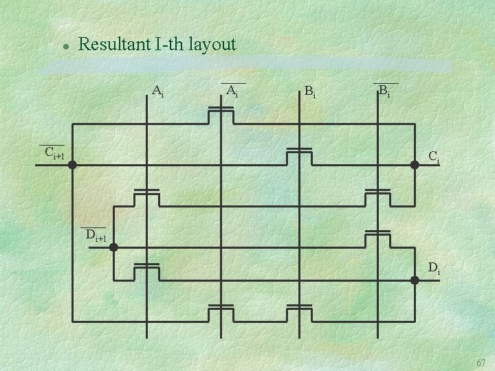
l Ex) Comparator An-1 Cn((=0) Dn(=0) Aj Aj A 0 Cn Cj+1 Cj C 1 C 0 Dn Dj+1 Dj D 1 D 0 Bn-1 Bj Bj B 0 1) Cn=0, Dn =0 3) C 0 becomes 1 when A>B 2) For cell I, D 0 becomes 1 when A<B Ci =1 when Ci+1 =1, or C 0 and D 0 are both 0 when A=B Ai > Bi and Di+1 =0 Di =1 when Di+1 =1, or Ai > Bi and Ci+1 =0 64
Ai. Bi 00 A 01 B B A C C A 10 B 11 A C D B B D 10 A C D B B D C C D D d A C B D d 11 B D A Ci+1 Di+1 not exist 01 D B C D 65
Ai. Bi 00 A 01 B B A C C A 10 B 11 A C D B B D 10 A C D B B D C C D D d A C B D d 11 B D A Ci+1 Di+1 not exist 01 D B C D 66
l Resultant I-th layout Ai Ci+1 Ai Bi Bi Ci Di+1 Di 67
5. Bi. CMOS logic q Comparison of CMOS vs. Bipolar ECL (Emitter-Coupled Logic) CMOS ECL Adv. high, symm noise margin high input impedance high gain in transition region high packing density low power consumption high current drive per unit area high switching speed low I/O noise Low speed(esp. for large C) High power consumption large area low input impedance smaller noise margin Disad. 68
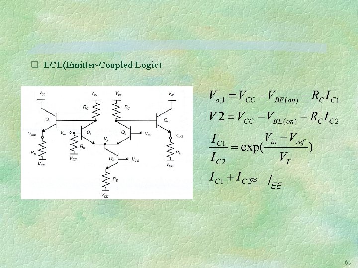
q ECL(Emitter-Coupled Logic) 69
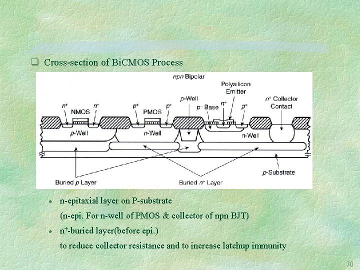
q Cross-section of Bi. CMOS Process l n-epitaxial layer on P-substrate (n-epi. For n-well of PMOS & collector of npn BJT) l n+-buried layer(before epi. ) to reduce collector resistance and to increase latchup immunity 70
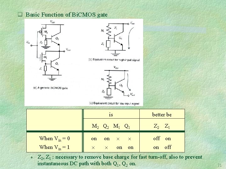
q Basic Function of Bi. CMOS gate is better be M 2 Q 2 M 1 Q 1 l Z 2 Z 1 When Vin = 0 on on off on When Vin = 1 on on on off Z 2, Z 1 : necessary to remove base charge for fast turn-off, also to prevent instantaneous DC path with both Q 1, Q 2 on. 71
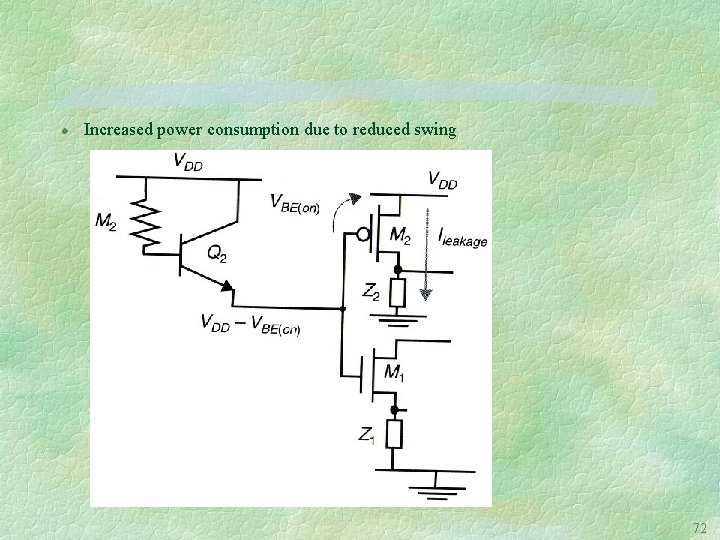
l Increased power consumption due to reduced swing 72
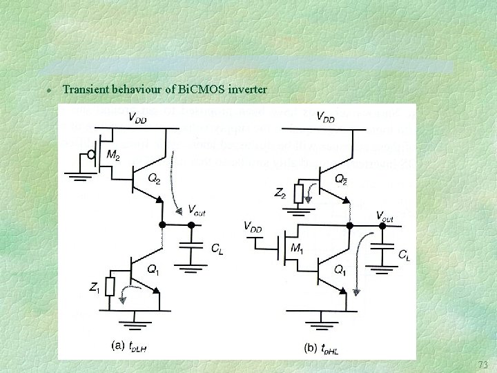
l Transient behaviour of Bi. CMOS inverter 73
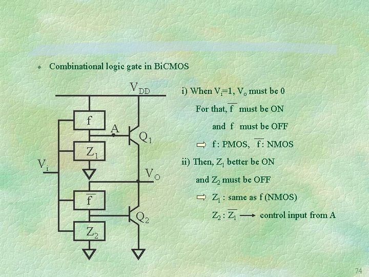
l Combinational logic gate in Bi. CMOS VDD f Vi Z 1 For that, f must be ON A Q 1 VO and f must be OFF f : PMOS, f : NMOS ii) Then, Z 1 better be ON and Z 2 must be OFF Z 1 : same as f (NMOS) f Z 2 i) When Vi=1, Vo must be 0 Q 2 Z 2 : Z 1 control input from A 74
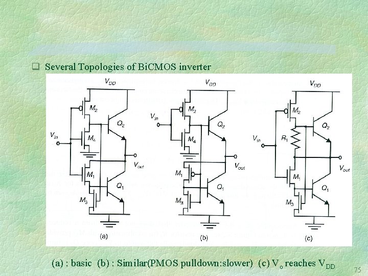
q Several Topologies of Bi. CMOS inverter (a) : basic (b) : Similar(PMOS pulldown: slower) (c) Vo reaches VDD 75
![(d) Feed Z 1 into the Q 2 base ] Utilize charge removed from](http://slidetodoc.com/presentation_image_h2/7e2825e03741e36bb42e660180c521d3/image-76.jpg "(d) Feed Z 1 into the Q 2 base ] Utilize charge removed from")
(d) Feed Z 1 into the Q 2 base ] Utilize charge removed from Q 1 -base to turn on Q 2. 76
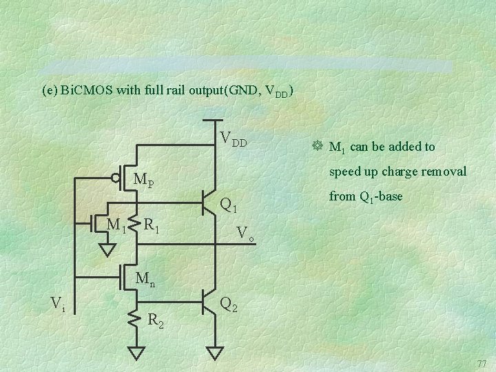
(e) Bi. CMOS with full rail output(GND, VDD) VDD speed up charge removal MP M 1 R 1 ] M 1 can be added to Q 1 from Q 1 -base Vo Mn Vi R 2 Q 2 77
![q NAND 2 Bi. CMOS gate ] For large fan-in, discharging Q 1 -base](http://slidetodoc.com/presentation_image_h2/7e2825e03741e36bb42e660180c521d3/image-78.jpg "q NAND 2 Bi. CMOS gate ] For large fan-in, discharging Q 1 -base")
q NAND 2 Bi. CMOS gate ] For large fan-in, discharging Q 1 -base is slow due to many parallel PMOSFET’S. 78
![q NOR 2 Bi. CMOS gate ] NAND is preferred over NOR in Bi.](http://slidetodoc.com/presentation_image_h2/7e2825e03741e36bb42e660180c521d3/image-79.jpg "q NOR 2 Bi. CMOS gate ] NAND is preferred over NOR in Bi.")
q NOR 2 Bi. CMOS gate ] NAND is preferred over NOR in Bi. CMOS logic, because charging through series PMOSFET’S is very slow 79
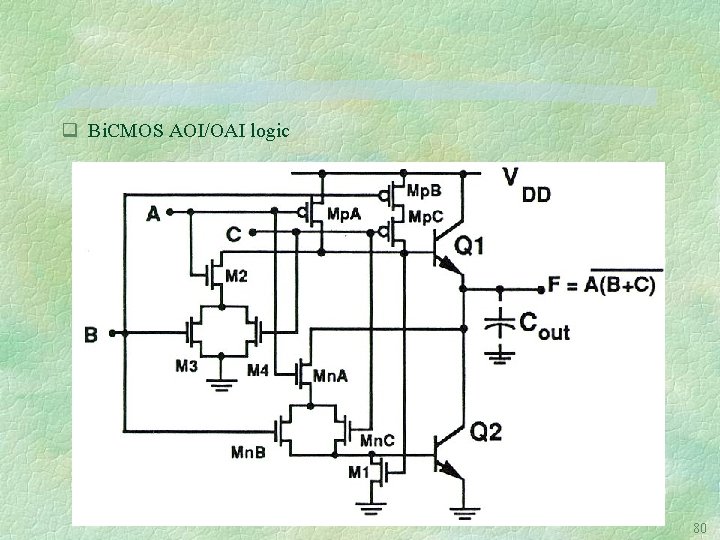
q Bi. CMOS AOI/OAI logic 80
![q Bi. CMOS to CMOS interface circuit ] One can connect PMOS output and](http://slidetodoc.com/presentation_image_h2/7e2825e03741e36bb42e660180c521d3/image-81.jpg "q Bi. CMOS to CMOS interface circuit ] One can connect PMOS output and")
q Bi. CMOS to CMOS interface circuit ] One can connect PMOS output and VDD. ] Connecting from Q 1 -base to feedback inverter is faster than connecting from Q 1 -emitter 81
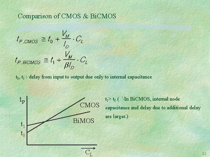
Comparison of CMOS & Bi. CMOS t 0, t 1 : delay from input to output due only to internal capacitance t 1 t 0 CMOS Bi. MOS CL t. P t 1> t 0 ( In Bi. CMOS, internal node capacitance and delay due to additional delay are larger. ) 82
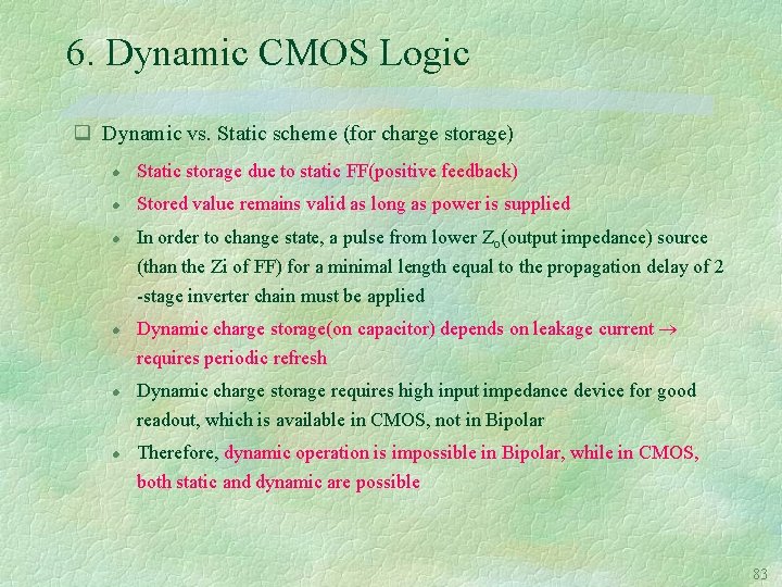
6. Dynamic CMOS Logic q Dynamic vs. Static scheme (for charge storage) l Static storage due to static FF(positive feedback) l Stored value remains valid as long as power is supplied l l In order to change state, a pulse from lower Zo(output impedance) source (than the Zi of FF) for a minimal length equal to the propagation delay of 2 -stage inverter chain must be applied Dynamic charge storage(on capacitor) depends on leakage current requires periodic refresh Dynamic charge storage requires high input impedance device for good readout, which is available in CMOS, not in Bipolar Therefore, dynamic operation is impossible in Bipolar, while in CMOS, both static and dynamic are possible 83
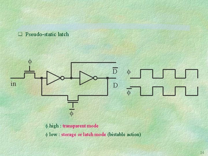
q Pseudo-static latch D in D high : transparent mode low : storage or latch mode (bistable action) 84
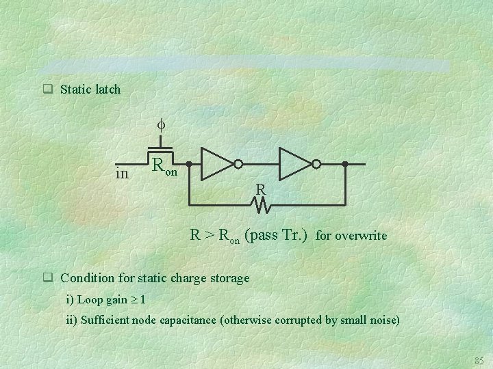
q Static latch in Ron R R > Ron (pass Tr. ) for overwrite q Condition for static charge storage i) Loop gain 1 ii) Sufficient node capacitance (otherwise corrupted by small noise) 85
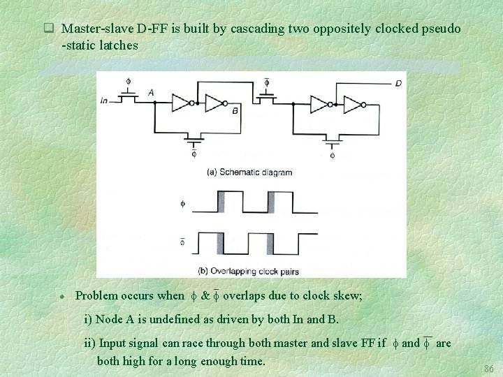
q Master-slave D-FF is built by cascading two oppositely clocked pseudo -static latches l Problem occurs when & overlaps due to clock skew; i) Node A is undefined as driven by both In and B. ii) Input signal can race through both master and slave FF if and are both high for a long enough time. 86
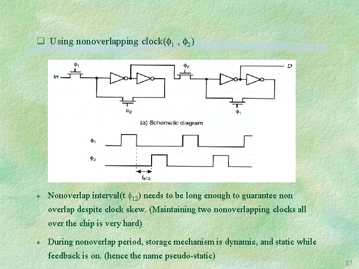
q Using nonoverlapping clock( 1 , 2) l Nonoverlap interval(t 12) needs to be long enough to guarantee non overlap despite clock skew. (Maintaining two nonoverlapping clocks all over the chip is very hard) l During nonoverlap period, storage mechanism is dynamic, and static while feedback is on. (hence the name pseudo-static) 87
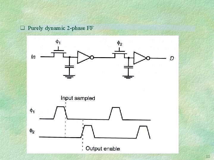
q Purely dynamic 2 -phase FF 88
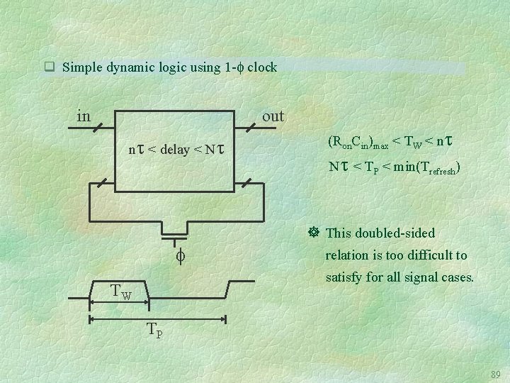
q Simple dynamic logic using 1 - clock in out n < delay < N (Ron. Cin)max < TW < n N < TP < min(Trefresh) ] This doubled-sided relation is too difficult to satisfy for all signal cases. TW TP 89
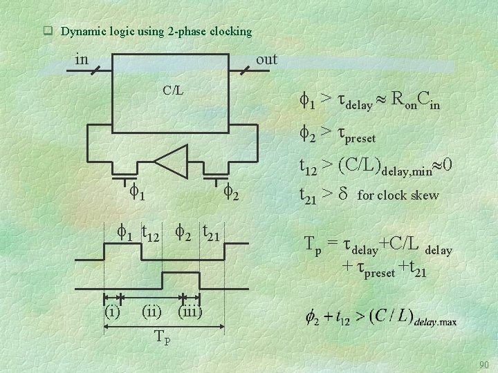
q Dynamic logic using 2 -phase clocking in out C/L 1 > delay Ron. Cin 2 > preset 1 1 t 12 2 t 21 (i) 2 t 12 > (C/L)delay, min 0 t 21 > for clock skew Tp = delay+C/L delay + preset +t 21 (ii) (iii) TP 90
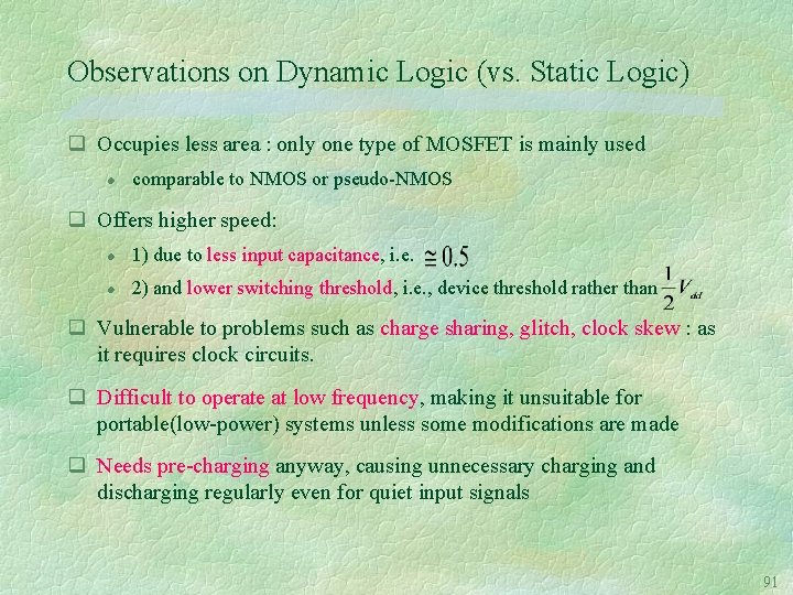
Observations on Dynamic Logic (vs. Static Logic) q Occupies less area : only one type of MOSFET is mainly used l comparable to NMOS or pseudo-NMOS q Offers higher speed: l 1) due to less input capacitance, i. e. l 2) and lower switching threshold, i. e. , device threshold rather than q Vulnerable to problems such as charge sharing, glitch, clock skew : as it requires clock circuits. q Difficult to operate at low frequency, making it unsuitable for portable(low-power) systems unless some modifications are made q Needs pre-charging anyway, causing unnecessary charging and discharging regularly even for quiet input signals 91
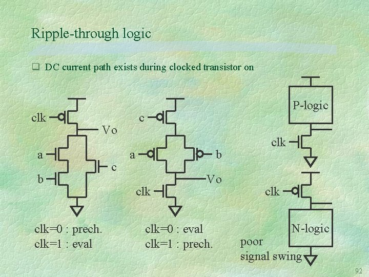
Ripple-through logic q DC current path exists during clocked transistor on clk c Vo a b clk=0 : prech. clk=1 : eval c P-logic a b clk Vo clk=0 : eval clk=1 : prech. clk N-logic poor signal swing 92
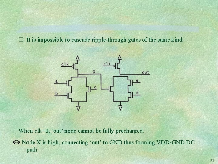
q It is impossible to cascade ripple-through gates of the same kind. When clk=0, ‘out’ node cannot be fully precharged. Node X is high, connecting ‘out’ to GND thus forming VDD-GND DC path 93
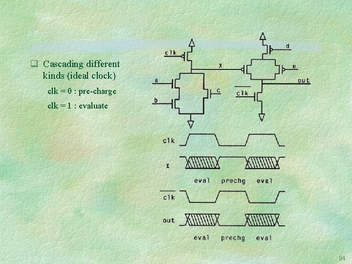
q Cascading different kinds (ideal clock) clk = 0 : pre-charge clk = 1 : evaluate 94
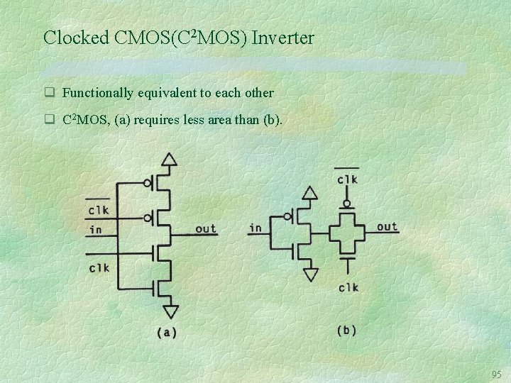
Clocked CMOS(C 2 MOS) Inverter q Functionally equivalent to each other q C 2 MOS, (a) requires less area than (b). 95
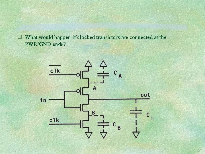
q What would happen if clocked transistors are connected at the PWR/GND ends? 96
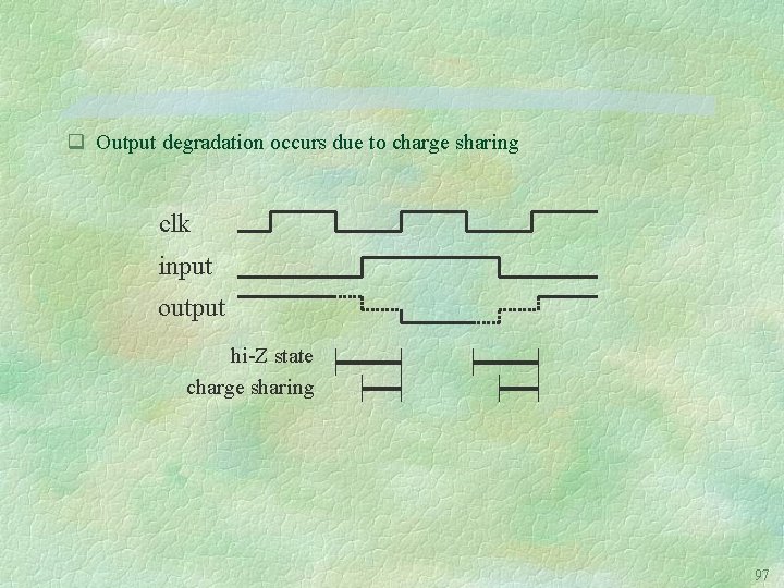
q Output degradation occurs due to charge sharing clk input output hi-Z state charge sharing 97
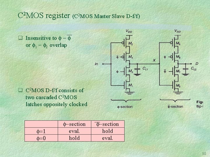
C 2 MOS register (C 2 MOS Master Slave D-f/f) q Insensitive to or 1 2 overlap q C 2 MOS D-f/f consists of two cascaded C 2 MOS latches oppositely clocked =1 =0 section eval. hold section hold eval. 98
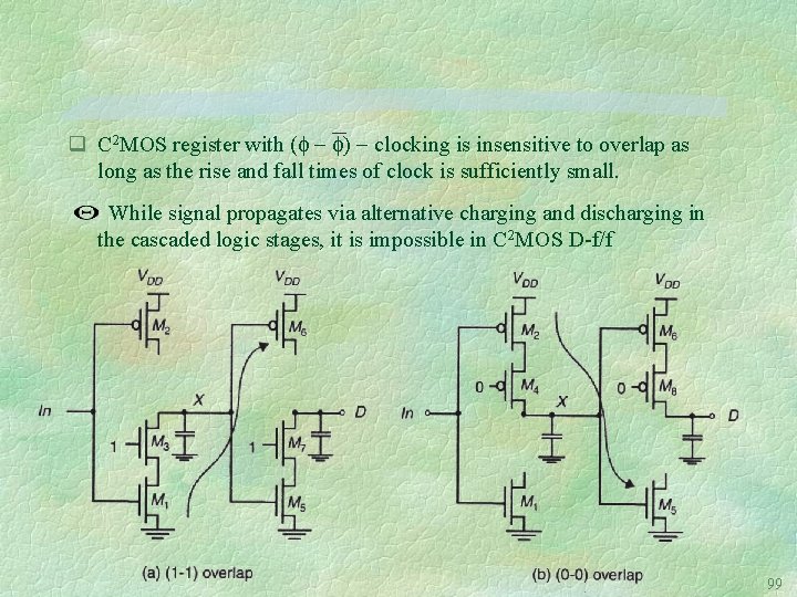
q C 2 MOS register with ( ) clocking is insensitive to overlap as long as the rise and fall times of clock is sufficiently small. While signal propagates via alternative charging and discharging in the cascaded logic stages, it is impossible in C 2 MOS D-f/f 99
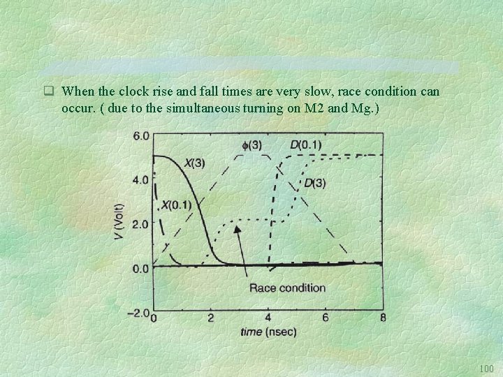
q When the clock rise and fall times are very slow, race condition can occur. ( due to the simultaneous turning on M 2 and Mg. ) 100
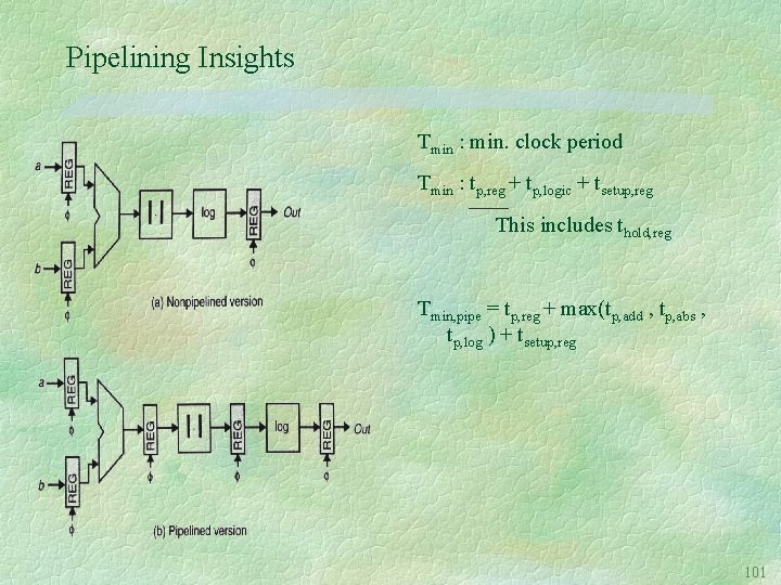
Pipelining Insights Tmin : min. clock period Tmin : tp, reg + tp, logic + tsetup, reg This includes thold, reg Tmin, pipe = tp, reg + max(tp, add , tp, abs , tp, log ) + tsetup, reg 101
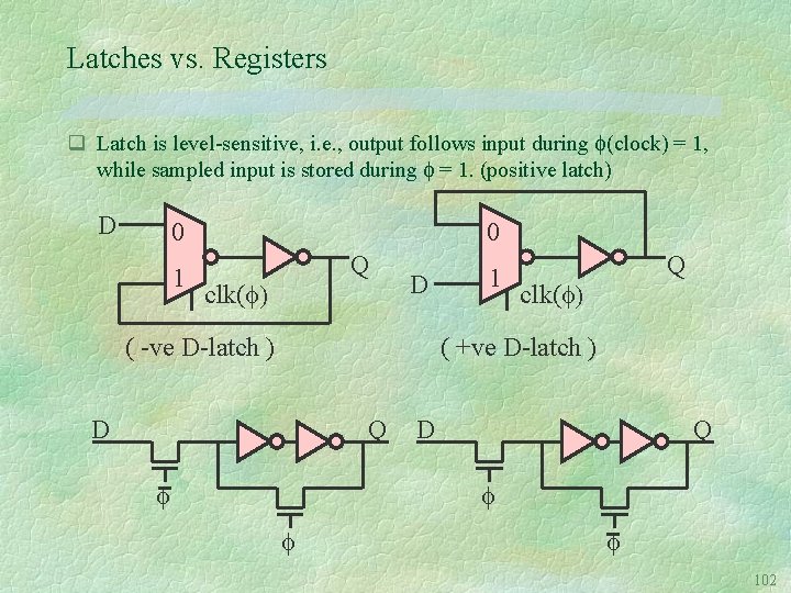
Latches vs. Registers q Latch is level-sensitive, i. e. , output follows input during (clock) = 1, while sampled input is stored during = 1. (positive latch) D 0 1 0 Q clk( ) D ( -ve D-latch ) 1 Q clk( ) ( +ve D-latch ) D Q 102
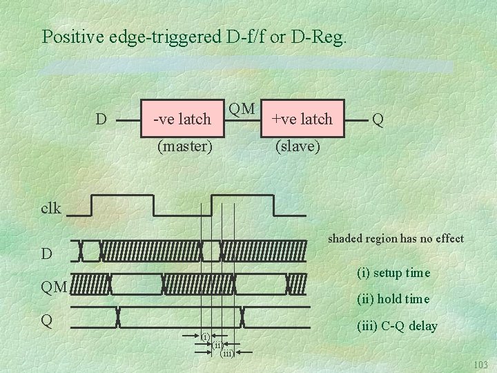
Positive edge-triggered D-f/f or D-Reg. D QM -ve latch (master) +ve latch Q (slave) clk shaded region has no effect D (i) setup time QM (ii) hold time Q (i) (iii) C-Q delay (ii) (iii) 103
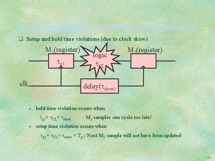
q Setup and hold time violations (due to clock skew) M 1(register) g 1 clk logic CL M 2(register) delay( skew) l hold time violation occurs when g 1+ CL< skew l : M 2 samples one cycle too late! setup time violation occurs when g 1+ CL> skew + Tp : Next M 2 sample will not have been updated 104
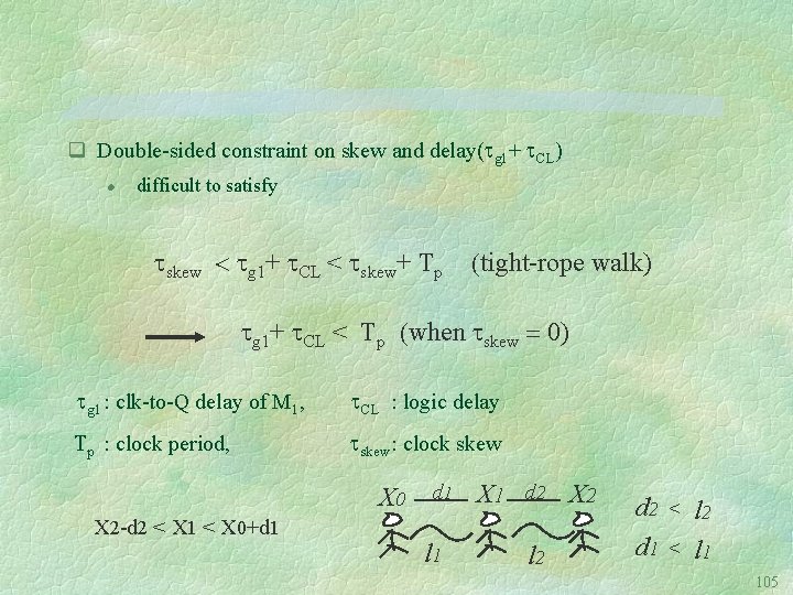
q Double-sided constraint on skew and delay( g 1+ CL) l difficult to satisfy skew < g 1+ CL < skew+ Tp (tight-rope walk) g 1+ CL < Tp (when skew = 0) g 1 : clk-to-Q delay of M 1, CL : logic delay Tp : clock period, skew : clock skew X 0 X 2 -d 2 < X 1 < X 0+d 1 l 1 X 1 d 2 X 2 l 2 d 1 < l 2 < l 1 105
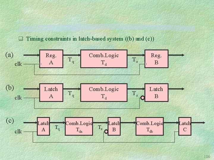
q Timing constraints in latch-based system ((b) and (c)) (a) clk Reg. A clk Latch A (b) (c) clk Latch Tq A Tq Comb. Logic Td Comb. Logic Ts Tda Latch B Ts Reg. B Ts Latch B Comb. Logic Tdb Latch C 106
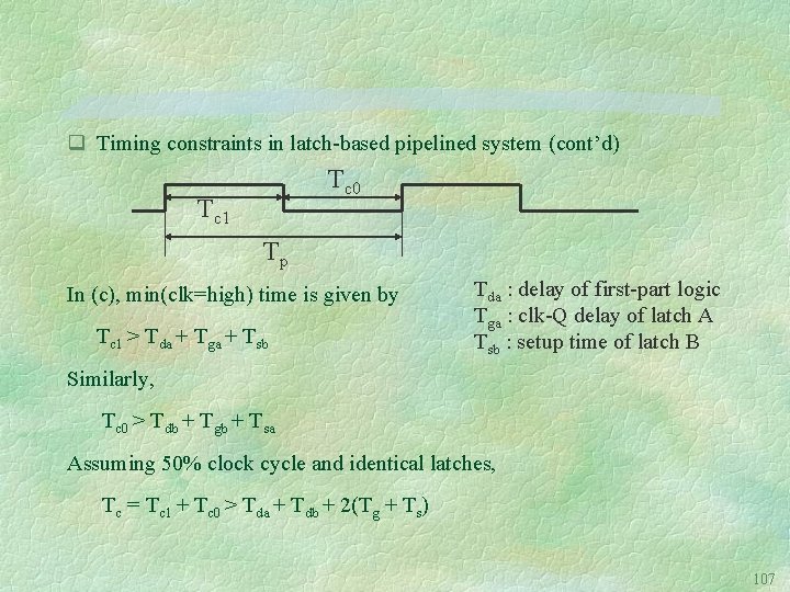
q Timing constraints in latch-based pipelined system (cont’d) Tc 0 Tc 1 Tp In (c), min(clk=high) time is given by Tc 1 > Tda + Tga + Tsb Tda : delay of first-part logic Tga : clk-Q delay of latch A Tsb : setup time of latch B Similarly, Tc 0 > Tdb + Tgb + Tsa Assuming 50% clock cycle and identical latches, Tc = Tc 1 + Tc 0 > Tda + Tdb + 2(Tg + Ts) 107
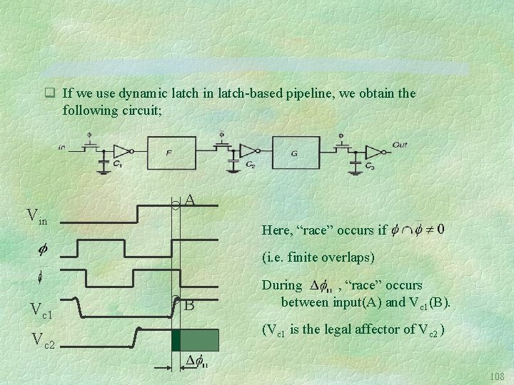
q If we use dynamic latch in latch-based pipeline, we obtain the following circuit; Vin A Here, “race” occurs if (i. e. finite overlaps) Vc 1 Vc 2 B During , “race” occurs between input(A) and Vc 1(B). (Vc 1 is the legal affector of Vc 2 ) 108
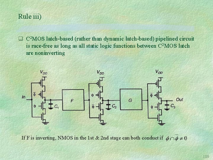
Rule iii) q C 2 MOS latch-based (rather than dynamic latch-based) pipelined circuit is race-free as long as all static logic functions between C 2 MOS latch are noninverting If F is inverting, NMOS in the 1 st & 2 nd stage can both conduct if 109
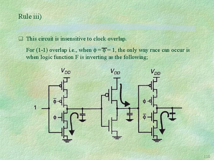
Rule iii) q This circuit is insensitive to clock overlap. For (1 -1) overlap i. e. , when = = 1, the only way race can occur is when logic function F is inverting as the following; 110
q NORA(NO-RAce) CMOS and rules to prevent RACE i) consists of i) C 2 MOS pipeline registers, and ii) NP-CMOS dynamic functional block modules. ii) Each block module is a combinational logic followed by a C 2 MOS latch. (Generalization) Each combinational logic is a cascade of an appropriate number(being limited by clock period) of either static or dynamic logic stages. iii) Number of static inversions between C 2 MOS latches should be even iv) Same(opposite) type of two dynamic logic stages need an odd (even) number of static inversions between them. v) Number of static inversions between the last dynamic and the C 2 MOS latch must be even for race-free. 111
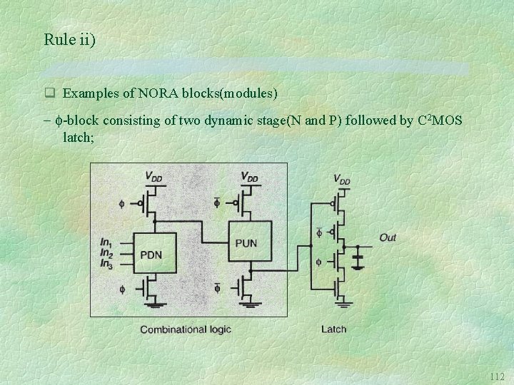
Rule ii) q Examples of NORA blocks(modules) -block consisting of two dynamic stage(N and P) followed by C 2 MOS latch; 112
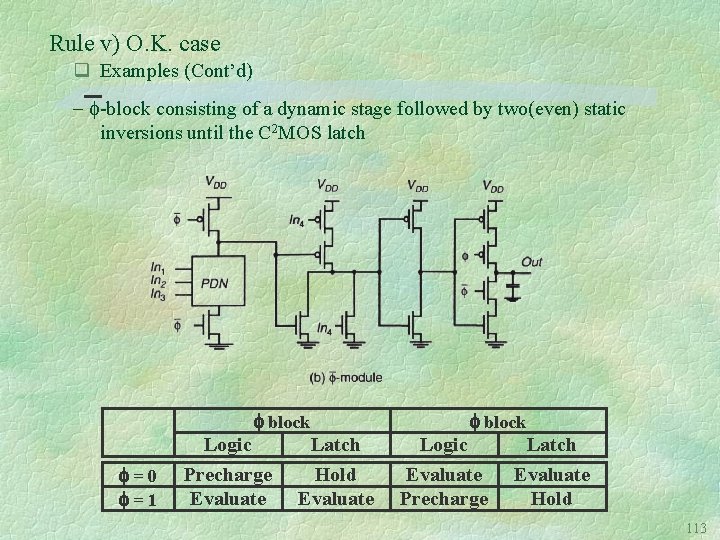
Rule v) O. K. case q Examples (Cont’d) -block consisting of a dynamic stage followed by two(even) static inversions until the C 2 MOS latch block =0 =1 Logic Precharge Evaluate Latch Hold Evaluate block Logic Evaluate Precharge Latch Evaluate Hold 113
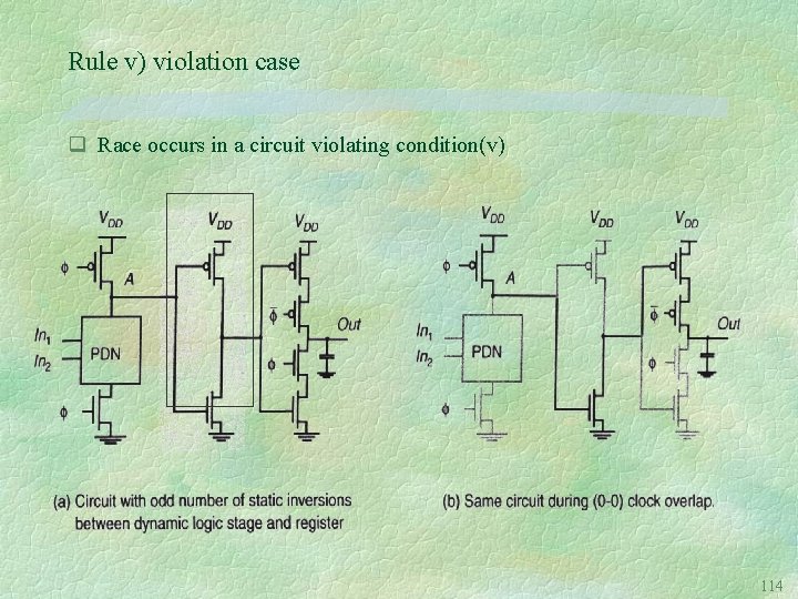
Rule v) violation case q Race occurs in a circuit violating condition(v) 114
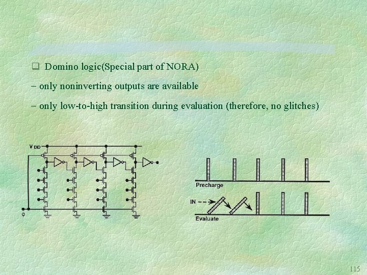
q Domino logic(Special part of NORA) only noninverting outputs are available only low-to-high transition during evaluation (therefore, no glitches) 115
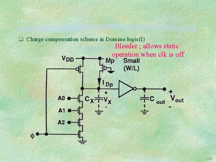
q Charge compensation scheme in Domino logic(I) Bleeder ; allows static operation when clk is off 116
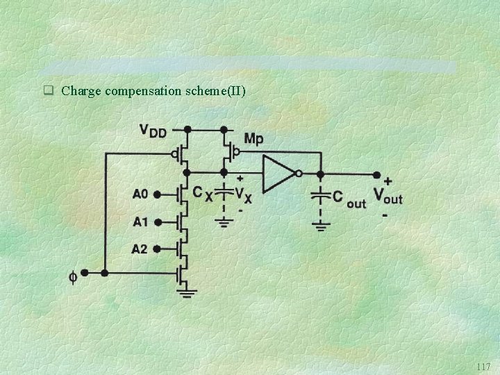
q Charge compensation scheme(II) 117
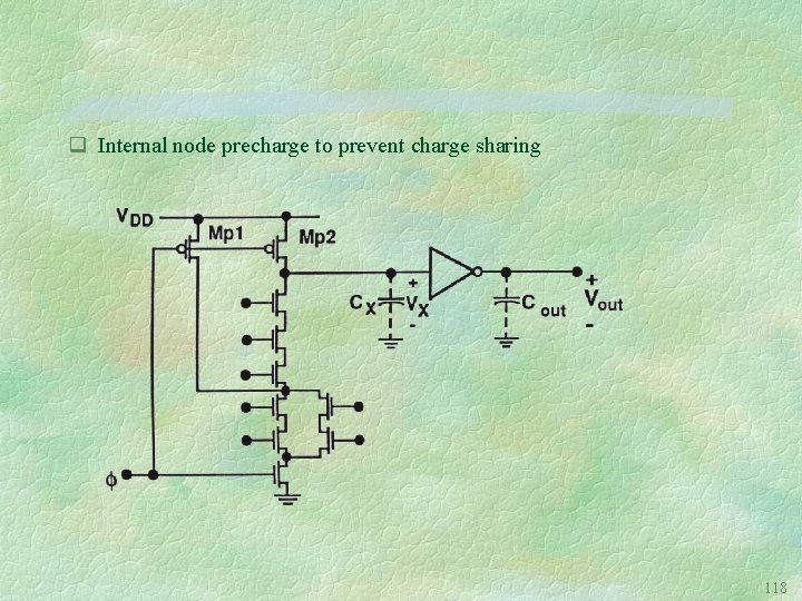
q Internal node precharge to prevent charge sharing 118
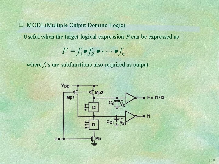
q MODL(Multiple Output Domino Logic) Useful when the target logical expression F can be expressed as F = f 1 f 2 f n where fi’s are subfunctions also required as output 119
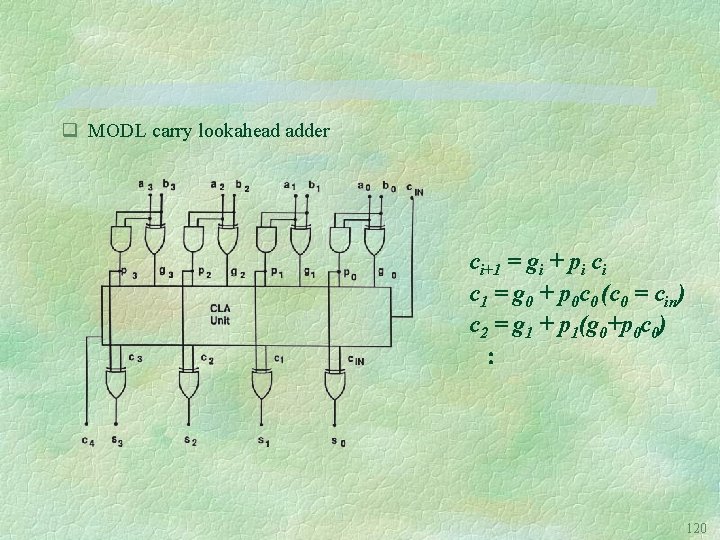
q MODL carry lookahead adder ci+1 = gi + pi ci c 1 = g 0 + p 0 c 0 (c 0 = cin) c 2 = g 1 + p 1(g 0+p 0 c 0) 120
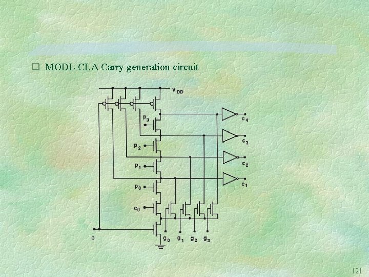
q MODL CLA Carry generation circuit 121
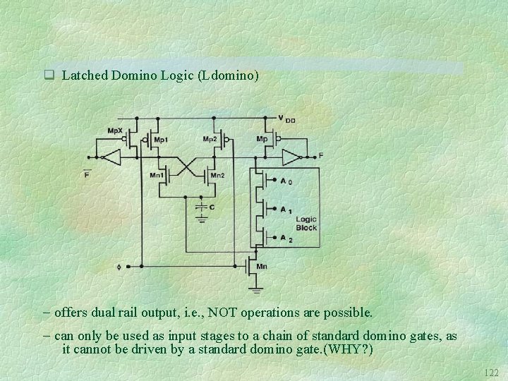
q Latched Domino Logic (Ldomino) offers dual rail output, i. e. , NOT operations are possible. can only be used as input stages to a chain of standard domino gates, as it cannot be driven by a standard domino gate. (WHY? ) 122
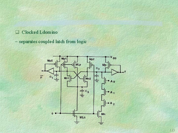
q Clocked Ldomino separates coupled latch from logic 123
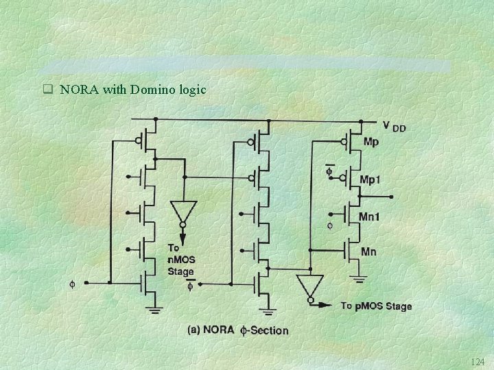
q NORA with Domino logic 124
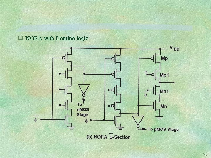
q NORA with Domino logic 125
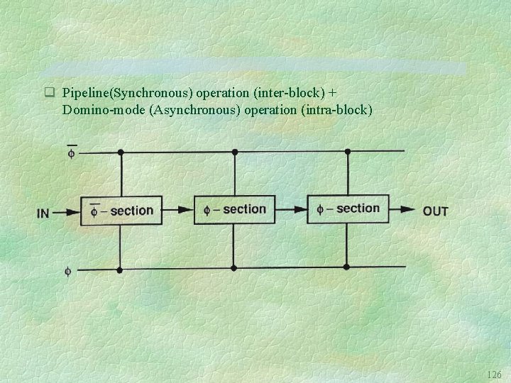
q Pipeline(Synchronous) operation (inter-block) + Domino-mode (Asynchronous) operation (intra-block) 126
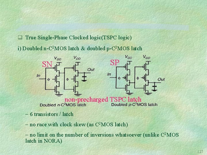
q True Single-Phase Clocked logic(TSPC logic) i) Doubled n-C 2 MOS latch & doubled p-C 2 MOS latch SP SN non-precharged TSPC latch 6 transistors / latch no race with clock skew (as C 2 MOS latch) no limit on the number of inversions whatsoever (unlike C 2 MOS latch in NORA) 127
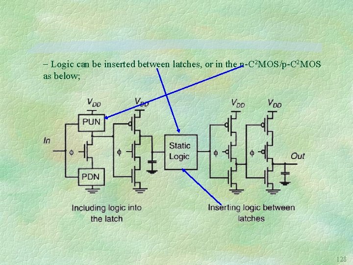
Logic can be inserted between latches, or in the n-C 2 MOS/p-C 2 MOS as below; 128
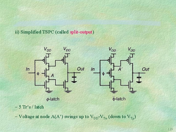
ii) Simplified TSPC (called split-output) 5 Tr’s / latch Voltage at node A(A’) swings up to VDD-VTn (down to VTp) 129
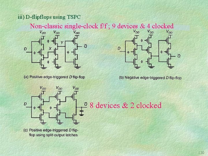
iii) D-flipflops using TSPC Non-classic single-clock f/f ; 9 devices & 4 clocked 8 devices & 2 clocked 130
iv) Some remarks on TSPC; Successfully used for very high-speed CMOS circuits such as Alpha chip (200 MHz in 0. 75 m technology) Clock slope should be sufficiently steep to prevent both PMOS and NMOS on, resulting in undefined outputs and race conditions. TSPC is vulnerable to noise, as TSPC register is dynamic and the impedance of the storage node is high. Often a feedback transistor is added to make it possible 131
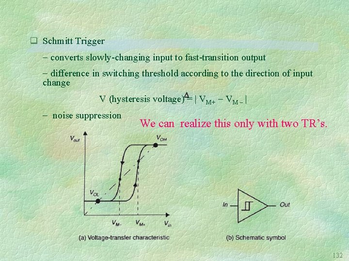
q Schmitt Trigger converts slowly-changing input to fast-transition output difference in switching threshold according to the direction of input change V (hysteresis voltage) = | VM+ VM | noise suppression We can realize this only with two TR’s. 132
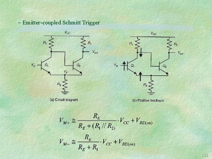
Emitter-coupled Schmitt Trigger 133
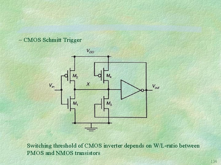
CMOS Schmitt Trigger Switching threshold of CMOS inverter depends on W/L-ratio between PMOS and NMOS transistors 134
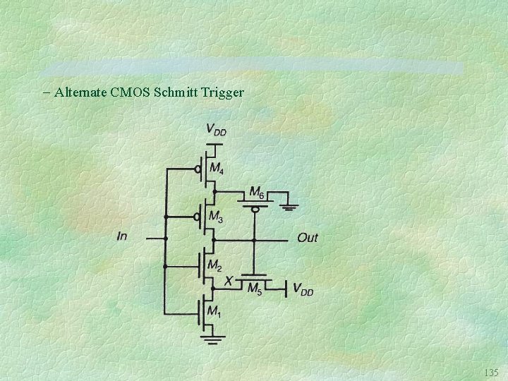
Alternate CMOS Schmitt Trigger 135
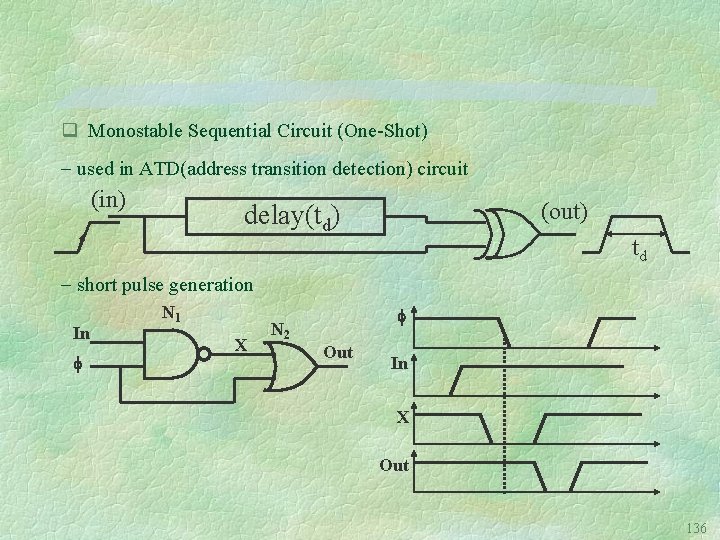
q Monostable Sequential Circuit (One-Shot) used in ATD(address transition detection) circuit (in) (out) delay(td) td short pulse generation In N 1 X N 2 Out In X Out 136
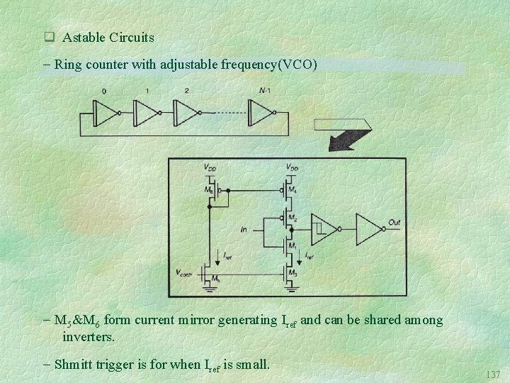
q Astable Circuits Ring counter with adjustable frequency(VCO) M 5&M 6 form current mirror generating Iref and can be shared among inverters. Shmitt trigger is for when Iref is small. 137



- Slides: 140