CMOS Digital Integrated Circuits Lec 6 CMOS Inverters
- Slides: 18

CMOS Digital Integrated Circuits Lec 6 CMOS Inverters: Static Characteristics 1 CMOS Digital Integrated Circuits

CMOS Inverters – Static Design n Goals • Understand the basic definition of basic circuit-level parameters. • Understand the VTC of a CMOS inverter. • Understand in detail static analysis of the CMOS inverter including circuit parameters, VOL, VOH, VIL, VIH, NML, and Vth 2 CMOS Digital Integrated Circuits

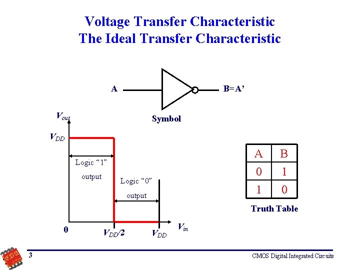
Voltage Transfer Characteristic The Ideal Transfer Characteristic A B=A’ Vout Symbol VDD A 0 1 Logic “ 1” output Logic “ 0” output B 1 0 Truth Table 0 3 VDD/2 VDD Vin CMOS Digital Integrated Circuits

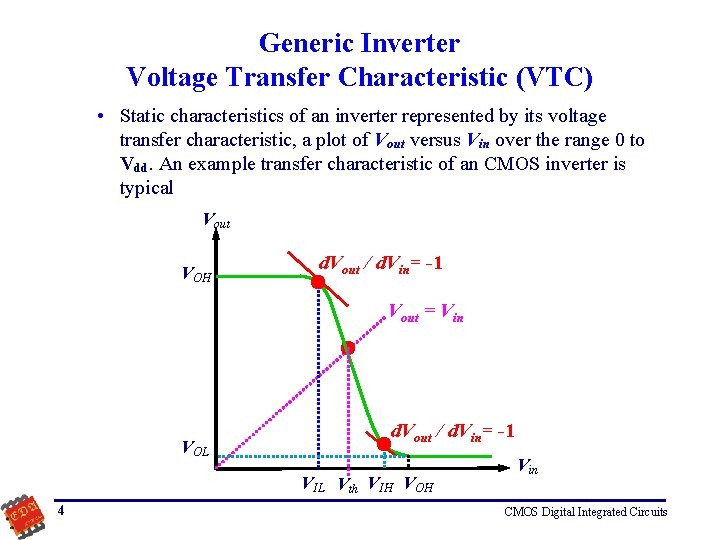
Generic Inverter Voltage Transfer Characteristic (VTC) • Static characteristics of an inverter represented by its voltage transfer characteristic, a plot of Vout versus Vin over the range 0 to Vdd. An example transfer characteristic of an CMOS inverter is typical Vout VOH d. Vout / d. Vin= -1 Vout = Vin VOL d. Vout / d. Vin= -1 VIL Vth VIH VOH 4 Vin CMOS Digital Integrated Circuits

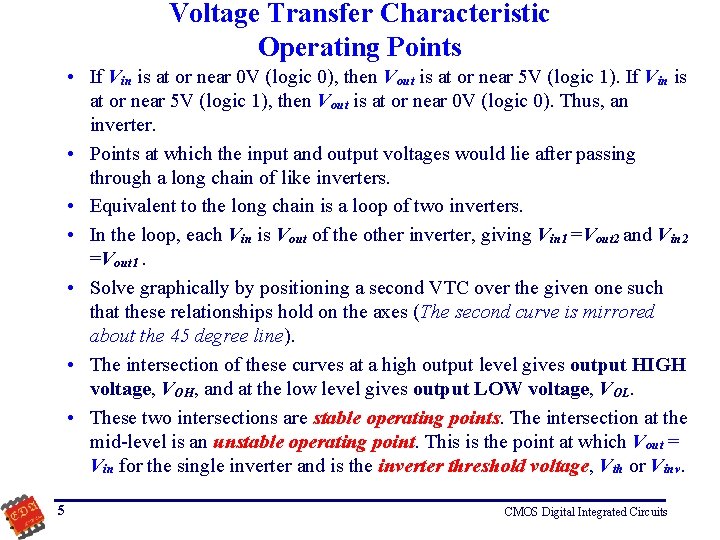
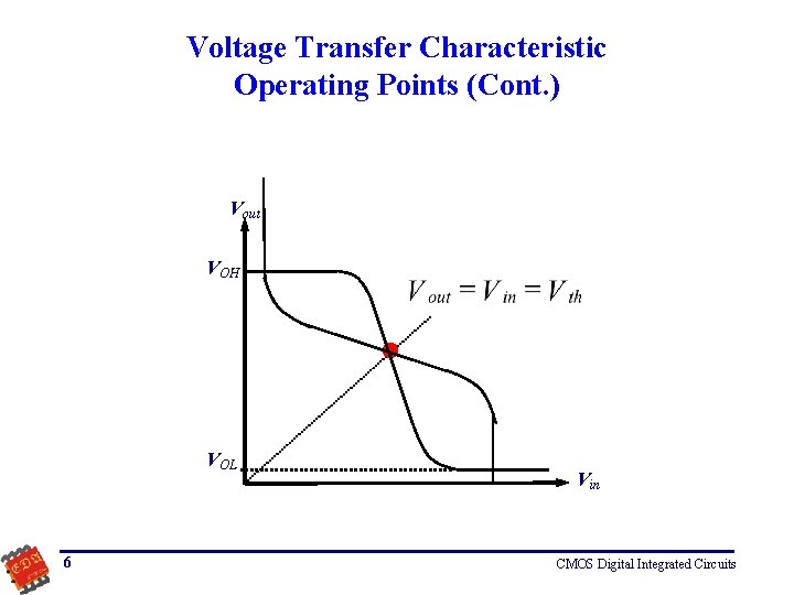
Voltage Transfer Characteristic Operating Points • If Vin is at or near 0 V (logic 0), then Vout is at or near 5 V (logic 1). If Vin is at or near 5 V (logic 1), then Vout is at or near 0 V (logic 0). Thus, an inverter. • Points at which the input and output voltages would lie after passing through a long chain of like inverters. • Equivalent to the long chain is a loop of two inverters. • In the loop, each Vin is Vout of the other inverter, giving Vin 1 =Vout 2 and Vin 2 =Vout 1. • Solve graphically by positioning a second VTC over the given one such that these relationships hold on the axes (The second curve is mirrored about the 45 degree line). • The intersection of these curves at a high output level gives output HIGH voltage, VOH, and at the low level gives output LOW voltage, VOL. • These two intersections are stable operating points. The intersection at the mid-level is an unstable operating point. This is the point at which Vout = Vin for the single inverter and is the inverter threshold voltage, Vth or Vinv. 5 CMOS Digital Integrated Circuits

Voltage Transfer Characteristic Operating Points (Cont. ) Vout VOH VOL 6 Vin CMOS Digital Integrated Circuits

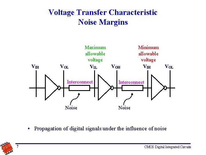
Voltage Transfer Characteristic Noise Margins VIH VOL Maximum allowable voltage VIL Interconnect Noise VOH Minimum allowable voltage VIH VOL Interconnect Noise • Propagation of digital signals under the influence of noise 7 CMOS Digital Integrated Circuits

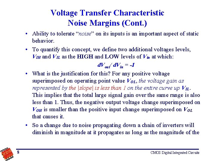
Voltage Transfer Characteristic Noise Margins (Cont. ) • Ability to tolerate “noise” on its inputs is an important aspect of static behavior. • To quantify this concept, we define two additional voltages levels, VIH and VIL as the HIGH and LOW levels of Vin at which: d. Vout/ d. Vin = -1 • What is the justification for this? For any positive voltage superimposed on operating point value VOL, the voltage gain as represented by the |slope| is less than 1 on the entire curve up VIL. This implies that the total large signal gain over the same range is also less than 1. Thus, the negative output voltage change superimposed on VOH is smaller than the positive input change superimposed on VOL that causes it. • So a change due to noise propagating down a chain of inverters will diminish in magnitude at it propagates as long as the magnitude of the 8 CMOS Digital Integrated Circuits

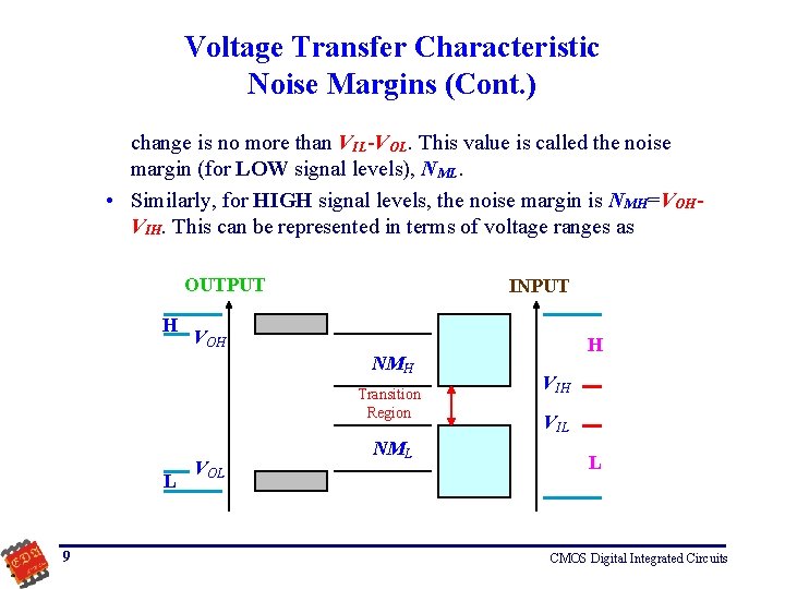
Voltage Transfer Characteristic Noise Margins (Cont. ) change is no more than VIL-VOL. This value is called the noise margin (for LOW signal levels), NML. • Similarly, for HIGH signal levels, the noise margin is NMH=VOHVIH. This can be represented in terms of voltage ranges as OUTPUT H INPUT VOH NMH Transition Region L 9 VOL NML H VIL L CMOS Digital Integrated Circuits

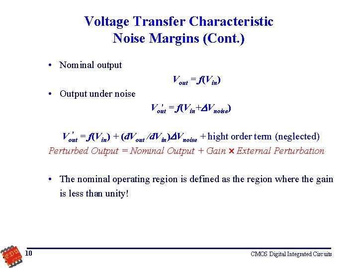
Voltage Transfer Characteristic Noise Margins (Cont. ) • Nominal output Vout = f(Vin) • Output under noise Vout = ׳ f(Vin+ Vnoise) = ׳ f(V ) + (d. V /d. V ) V Vout in noise + hight order term (neglected) Perturbed Output = Nominal Output + Gain External Perturbation • The nominal operating region is defined as the region where the gain is less than unity! 10 CMOS Digital Integrated Circuits

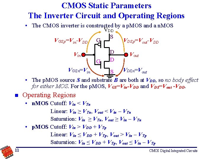
CMOS Static Parameters The Inverter Circuit and Operating Regions • The CMOS inverter is constructed by a p. MOS and a n. MOS VDD S VGS, p=Vin-VDD G VDS, p=Vout-VDD Vin G D D Vout VGS, n=Vin VDS, n=Vout S • The p. MOS source S and substrate B are both at VDD, so no body effect for either MOS. For the p. MOS, VGS=Vin-VDD and VDS=Vout -VDD. n Operating Regions • n. MOS Cutoff: Vin < VTn Linear: Vin ≥ VTn, Vout < Vin – VTn Saturation: Vin ≥ VTn, Vout ≥ Vin – VTn • p. MOS Cutoff: Vin > VDD + VTp Linear: Vin ≤ VDD + VTp, Vout > Vin – VTp Saturation: Vin ≤ VDD + VTp, Vout ≤ Vin – VTp 11 CMOS Digital Integrated Circuits

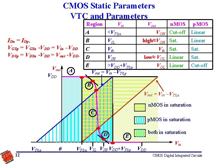
CMOS Static Parameters VTC and Parameters Region Vin A <VT 0, n IDn = IDp, B VGSp = VGSn -VDD = Vin –VDD C VDSp = VDSn -VDD = Vout -VDD. D Vout VDD A E Vout n. MOS VOH Cut-off VIL high≈VOH Sat. Vth Sat. VIH low≈ VOL Linear >VDD+VT 0, p Vout = Vin –VT 0, p VOL Linear p. MOS Linear Sat. Cut-off B Vout = Vin –VT 0, n n. MOS in saturation C p. MOS in saturation D VT 0, p 12 0 both in saturation E VT 0, n VIL VIH VDD+VT 0, p VDD Vin CMOS Digital Integrated Circuits

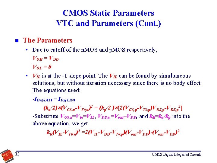
CMOS Static Parameters VTC and Parameters (Cont. ) n The Parameters • Due to cutoff of the n. MOS and p. MOS respectively, VOH = VDD VOL = 0 • VIL is at the -1 slope point. The VIL can be found by simultaneous solutions, but without iteration necessary since there is no body effect. The equations used: -IDn(SAT) = IDp(LIN) (kn/2) (VGS, n-VT 0, n)2 = (kp/2 ) [2(VGS, p-VT 0, p)VDS, p-VDS, p 2] -Substitute VGS, n=Vin=VIL, VDS, n =Vout–VDD, and k. R=kn/kp into the above equation, we get k. R(VIL-VT 0, n)2 =2(VIL-VDD-VT 0, p)(Vout-VDD)-(Vout-VDD)2 13 CMOS Digital Integrated Circuits

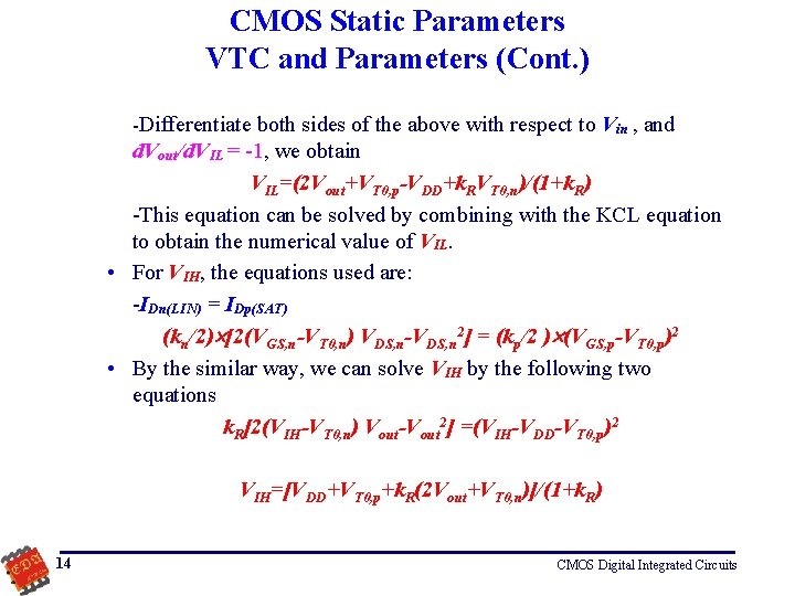
CMOS Static Parameters VTC and Parameters (Cont. ) -Differentiate both sides of the above with respect to Vin , and d. Vout/d. VIL = -1, we obtain VIL=(2 Vout+VT 0, p-VDD+k. RVT 0, n)/(1+k. R) -This equation can be solved by combining with the KCL equation to obtain the numerical value of VIL. • For VIH, the equations used are: -IDn(LIN) = IDp(SAT) (kn/2) [2(VGS, n-VT 0, n) VDS, n-VDS, n 2] = (kp/2 ) (VGS, p-VT 0, p)2 • By the similar way, we can solve VIH by the following two equations k. R[2(VIH-VT 0, n) Vout-Vout 2] =(VIH-VDD-VT 0, p)2 VIH=[VDD+VT 0, p+k. R(2 Vout+VT 0, n)]/(1+k. R) 14 CMOS Digital Integrated Circuits

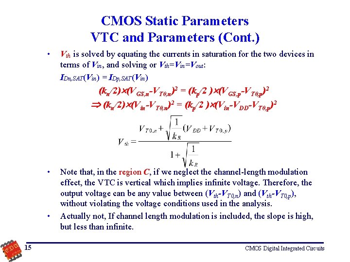
CMOS Static Parameters VTC and Parameters (Cont. ) • Vth is solved by equating the currents in saturation for the two devices in terms of Vin, and solving or Vth=Vin=Vout: IDn, SAT(Vin) = IDp, SAT(Vin) (kn/2) (VGS, n-VT 0, n)2 = (kp/2 ) (VGS, p-VT 0, p)2 (kn/2) (Vin-VT 0, n)2 = (kp/2 ) (Vin-VDD-VT 0, p)2 • • 15 Note that, in the region C, if we neglect the channel-length modulation effect, the VTC is vertical which implies infinite voltage. Therefore, the output voltage can be any value between (Vth-VT 0, n) and (Vth-VT 0, p), without violating the voltage conditions used in the analysis. Actually not, If channel length modulation is included, the slope is high, but less than infinite. CMOS Digital Integrated Circuits

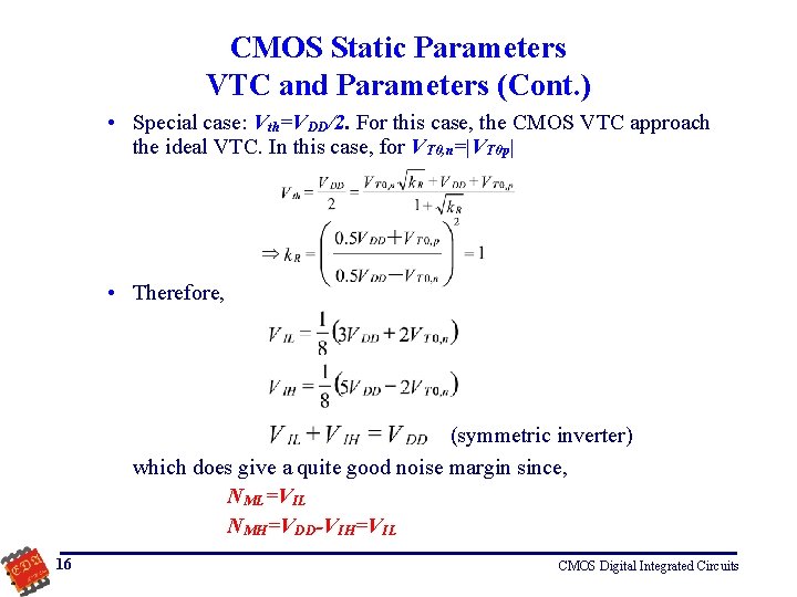
CMOS Static Parameters VTC and Parameters (Cont. ) • Special case: Vth=VDD/2. For this case, the CMOS VTC approach the ideal VTC. In this case, for VT 0, n=|VT 0 p| • Therefore, (symmetric inverter) which does give a quite good noise margin since, NML=VIL NMH=VDD-VIH=VIL 16 CMOS Digital Integrated Circuits

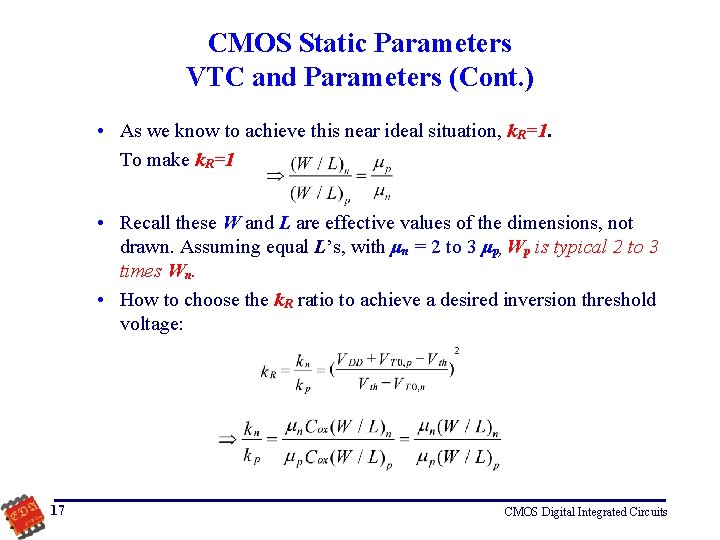
CMOS Static Parameters VTC and Parameters (Cont. ) • As we know to achieve this near ideal situation, k. R=1. To make k. R=1 • Recall these W and L are effective values of the dimensions, not drawn. Assuming equal L’s, with μn = 2 to 3 μp, Wp is typical 2 to 3 times Wn. • How to choose the k. R ratio to achieve a desired inversion threshold voltage: 17 CMOS Digital Integrated Circuits

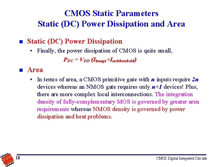
CMOS Static Parameters Static (DC) Power Dissipation and Area n Static (DC) Power Dissipation • Finally, the power dissipation of CMOS is quite small, PDC = VDD (Ileaage+Isubthreshold) n Area • In terms of area, a CMOS primitive gate with n inputs require 2 n devices whereas an NMOS gate requires only n+1 devices! Plus, there are more complex local interconnections. The integration density of fully-complementary MOS is governed by greater area requirements whereas NMOS density is governed by power dissipation and heat problems. 18 CMOS Digital Integrated Circuits