CMOS Digital Integrated Circuits Lec 14 LowPower CMOS
![Evolution in Power Density [W/cm²] 10000 Rocket Nozzle Sun‘s Surface? 1000 Nuclear Reactor 100 Evolution in Power Density [W/cm²] 10000 Rocket Nozzle Sun‘s Surface? 1000 Nuclear Reactor 100](https://slidetodoc.com/presentation_image_h/dbd503cee205a2aff5b87a22efe1fb64/image-3.jpg)
- Slides: 38

CMOS Digital Integrated Circuits Lec 14 Low-Power CMOS Logic Circuits 1 CMOS Digital Integrated Circuits

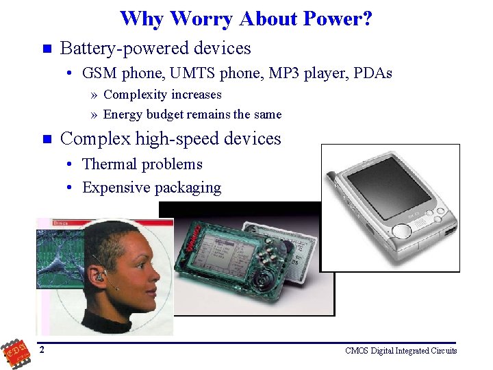
Why Worry About Power? n Battery-powered devices • GSM phone, UMTS phone, MP 3 player, PDAs » Complexity increases » Energy budget remains the same n Complex high-speed devices • Thermal problems • Expensive packaging 2 CMOS Digital Integrated Circuits
![Evolution in Power Density Wcm² 10000 Rocket Nozzle Suns Surface 1000 Nuclear Reactor 100 Evolution in Power Density [W/cm²] 10000 Rocket Nozzle Sun‘s Surface? 1000 Nuclear Reactor 100](https://slidetodoc.com/presentation_image_h/dbd503cee205a2aff5b87a22efe1fb64/image-3.jpg)
Evolution in Power Density [W/cm²] 10000 Rocket Nozzle Sun‘s Surface? 1000 Nuclear Reactor 100 Hot Plate 10 8086 4004 1 8080 8008 1970 286 P 6 386 Pentium® proc 486 8085 1980 1990 2000 2010 Source: adapted from Intel 3 CMOS Digital Integrated Circuits

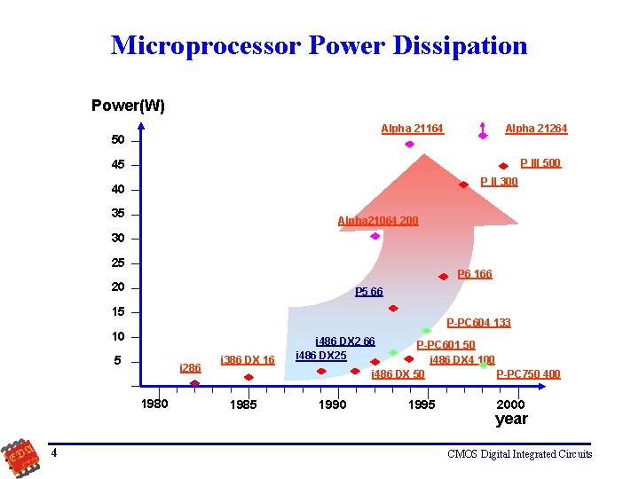
Microprocessor Power Dissipation Power(W) Alpha 21164 50 Alpha 21264 P III 500 45 P II 300 40 35 Alpha 21064 200 30 25 P 6 166 20 P 5 66 15 P-PC 604 133 10 5 i 286 1980 4 i 386 DX 16 1985 i 486 DX 2 66 i 486 DX 25 P-PC 601 50 i 486 DX 4 100 i 486 DX 50 P-PC 750 400 1995 2000 year CMOS Digital Integrated Circuits

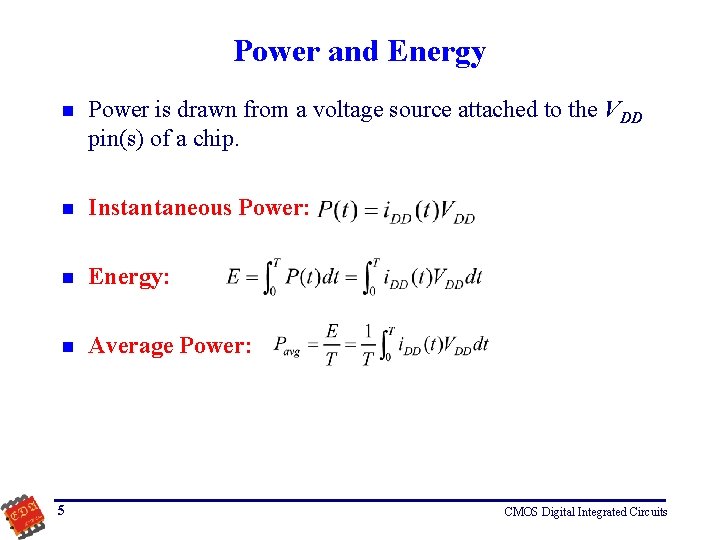
Power and Energy n Power is drawn from a voltage source attached to the VDD pin(s) of a chip. n Instantaneous Power: n Energy: n Average Power: 5 CMOS Digital Integrated Circuits

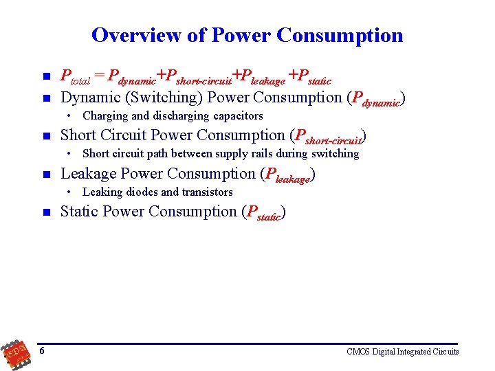
Overview of Power Consumption n n Ptotal = Pdynamic+Pshort-circuit+Pleakage +Pstatic Dynamic (Switching) Power Consumption (Pdynamic) • Charging and discharging capacitors n Short Circuit Power Consumption (Pshort-circuit) • Short circuit path between supply rails during switching n Leakage Power Consumption (Pleakage) • Leaking diodes and transistors n 6 Static Power Consumption (Pstatic) CMOS Digital Integrated Circuits

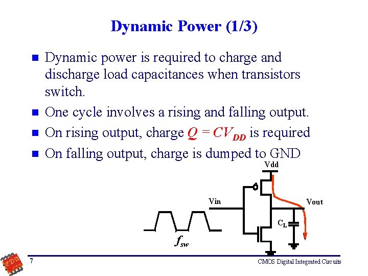
Dynamic Power (1/3) n n Dynamic power is required to charge and discharge load capacitances when transistors switch. One cycle involves a rising and falling output. On rising output, charge Q = CVDD is required On falling output, charge is dumped to GND Vdd Vin Vout CL fsw 7 CMOS Digital Integrated Circuits

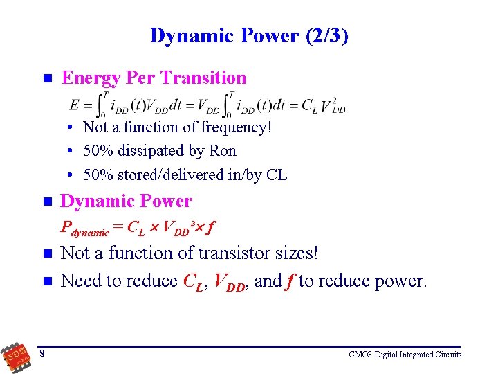
Dynamic Power (2/3) n Energy Per Transition • Not a function of frequency! • 50% dissipated by Ron • 50% stored/delivered in/by CL n Dynamic Power Pdynamic = CL VDD² f n n 8 Not a function of transistor sizes! Need to reduce CL, VDD, and f to reduce power. CMOS Digital Integrated Circuits

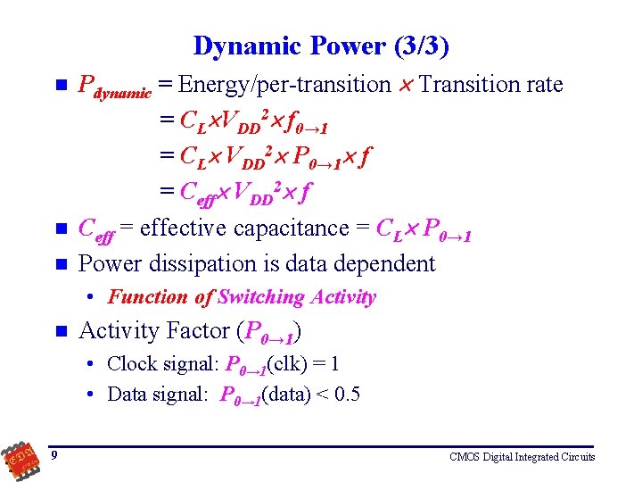
Dynamic Power (3/3) n n n Pdynamic = Energy/per-transition Transition rate = CL VDD 2 f 0→ 1 = CL VDD 2 P 0→ 1 f = Ceff VDD 2 f Ceff = effective capacitance = CL P 0→ 1 Power dissipation is data dependent • Function of Switching Activity n Activity Factor (P 0→ 1) • Clock signal: P 0→ 1(clk) = 1 • Data signal: P 0→ 1(data) < 0. 5 9 CMOS Digital Integrated Circuits

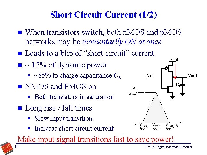
Short Circuit Current (1/2) n n n When transistors switch, both n. MOS and p. MOS networks may be momentarily ON at once Leads to a blip of “short circuit” current. Vdd ~ 15% of dynamic power • ~85% to charge capacitance CL n Vin NMOS and PMOS on Vout CL • Both transistors in saturation n Long rise / fall times • Slow input transition • Increase short circuit current Make input signal transitions fast to save power! 10 CMOS Digital Integrated Circuits

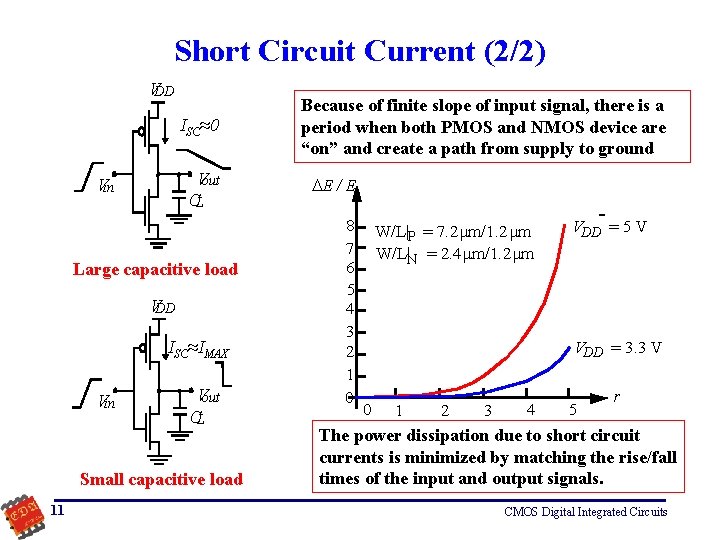
Short Circuit Current (2/2) VDD ISC≈0 Vout CL Vin Large capacitive load VDD ISC≈IMAX Vin Vout CL Small capacitive load 11 Because of finite slope of input signal, there is a period when both PMOS and NMOS device are “on” and create a path from supply to ground DE / E 8 7 6 5 4 3 2 1 0 W/L|P = 7. 2 mm/1. 2 mm W/L|N = 2. 4 mm/1. 2 mm VDD = 5 V VDD = 3. 3 V 0 1 2 3 4 5 r The power dissipation due to short circuit currents is minimized by matching the rise/fall times of the input and output signals. CMOS Digital Integrated Circuits

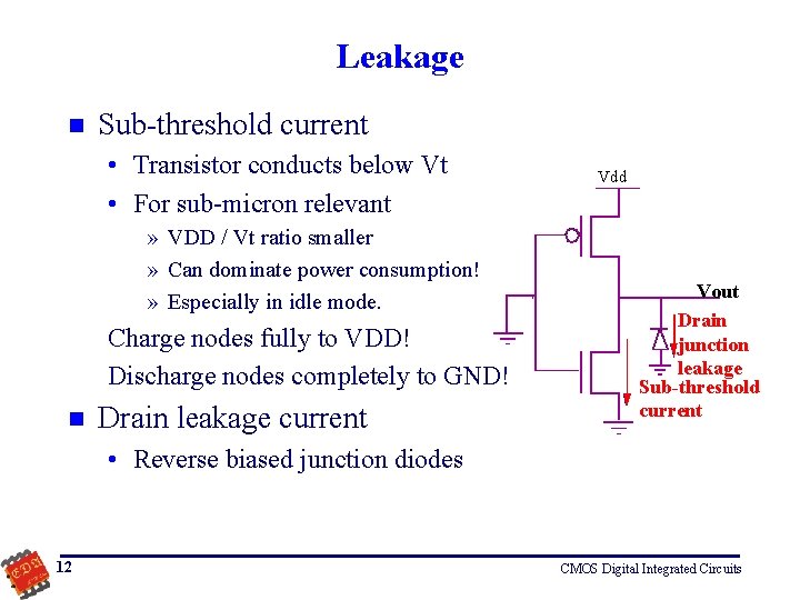
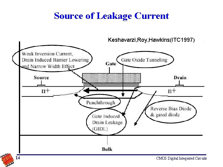
Leakage n Sub-threshold current • Transistor conducts below Vt • For sub-micron relevant » VDD / Vt ratio smaller » Can dominate power consumption! » Especially in idle mode. Charge nodes fully to VDD! Discharge nodes completely to GND! n Drain leakage current Vdd Vout Drain junction leakage Sub-threshold current • Reverse biased junction diodes 12 CMOS Digital Integrated Circuits

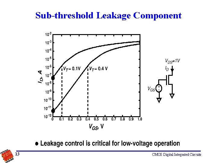
Sub-threshold Leakage Component 13 CMOS Digital Integrated Circuits

Source of Leakage Current Keshavarzi, Roy, Hawkins(ITC 1997) 14 CMOS Digital Integrated Circuits

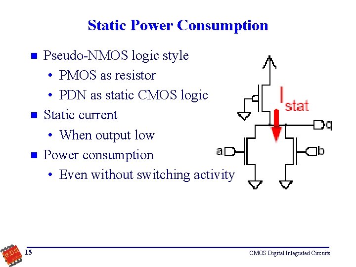
Static Power Consumption n 15 Pseudo-NMOS logic style • PMOS as resistor • PDN as static CMOS logic Static current • When output low Power consumption • Even without switching activity CMOS Digital Integrated Circuits

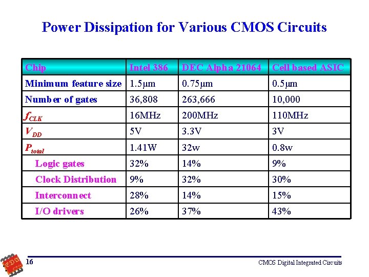
Power Dissipation for Various CMOS Circuits Chip DEC Alpha 21064 Cell based ASIC Minimum feature size 1. 5μm 0. 75μm 0. 5μm Number of gates 36, 808 263, 666 10, 000 f. CLK 16 MHz 200 MHz 110 MHz VDD 5 V 3. 3 V 3 V Ptotal 1. 41 W 32 w 0. 8 w Logic gates 32% 14% 9% Clock Distribution 9% 32% 30% Interconnect 28% 14% 15% I/O drivers 26% 37% 43% 16 Intel 386 CMOS Digital Integrated Circuits

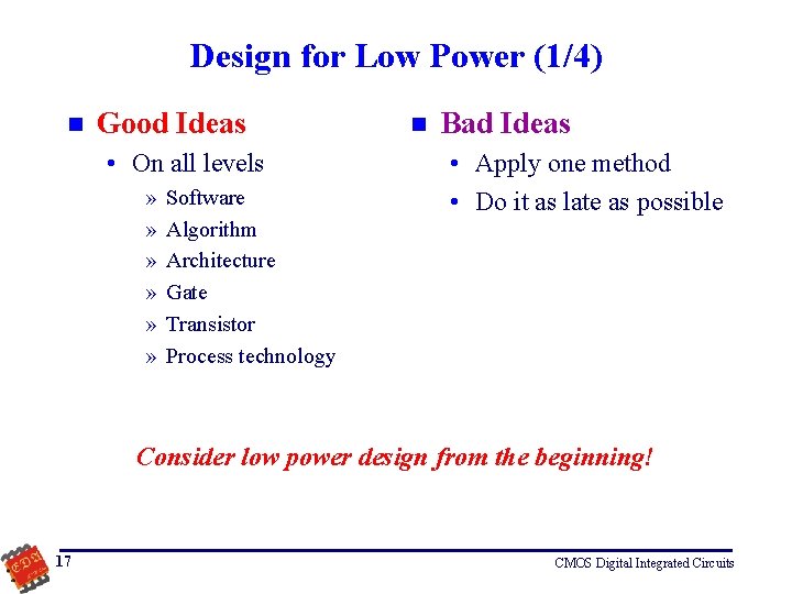
Design for Low Power (1/4) n Good Ideas • On all levels » » » Software Algorithm Architecture Gate Transistor Process technology n Bad Ideas • Apply one method • Do it as late as possible Consider low power design from the beginning! 17 CMOS Digital Integrated Circuits

Design for Low Power (2/4) n System Level • Power management » Power-down mode » Global clock gating » Dynamic voltage scaling • Hardware/software co-design » Early (simplified) power estimation » Partitioning of functionality » Minimum instructions for execution not code size 18 CMOS Digital Integrated Circuits

Design for Low Power (3/4) n Algorithm • Arithmetic » Choice of number representation » Pre-computation • Concurrency » Parallelism - Trade area for power » To reduce frequency 19 CMOS Digital Integrated Circuits

Design for Low Power (4/4) n Architecture • Pipelining » Allows voltage scaling: Increased throughput because frequency could be increased => lower supply voltage instead • Redundancy » Minimize shared resources to lower signal activity (buses) • Data encoding » Energy efficient state encoding » Example: Gray code, One hot encoding • Clocking » Gated clocks » Self-timed circuits 20 CMOS Digital Integrated Circuits

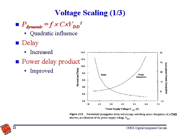
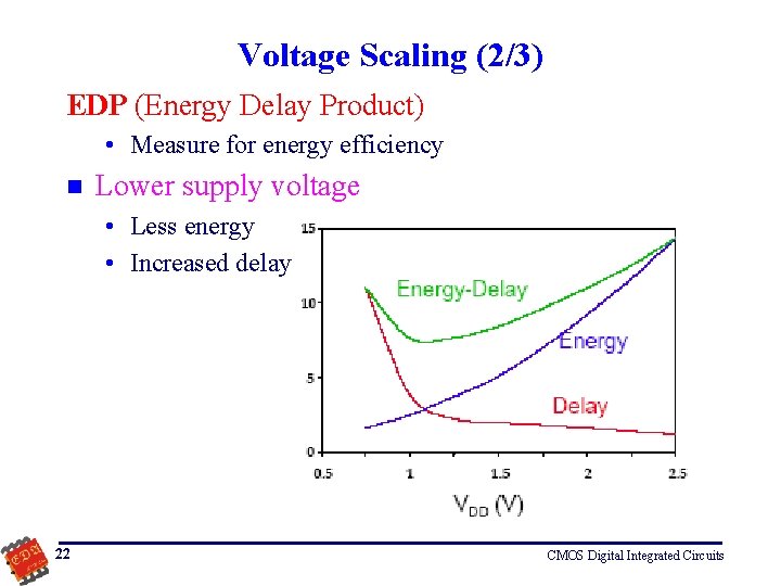
Voltage Scaling (1/3) n Pdynamic = f C VDD² • Quadratic influence n Delay • Increased n Power delay product • Improved 21 CMOS Digital Integrated Circuits

Voltage Scaling (2/3) EDP (Energy Delay Product) • Measure for energy efficiency n Lower supply voltage • Less energy • Increased delay 22 CMOS Digital Integrated Circuits

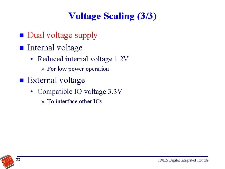
Voltage Scaling (3/3) n n Dual voltage supply Internal voltage • Reduced internal voltage 1. 2 V » For low power operation n External voltage • Compatible IO voltage 3. 3 V » To interface other ICs 23 CMOS Digital Integrated Circuits

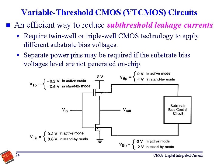
n Variable-Threshold CMOS (VTCMOS) Circuits An efficient way to reduce subthreshold leakage currents • Require twin-well or triple-well CMOS technology to apply different substrate bias voltages. • Separate power pins may be required if the substrate bias voltages level are not generated on-chip. 24 CMOS Digital Integrated Circuits

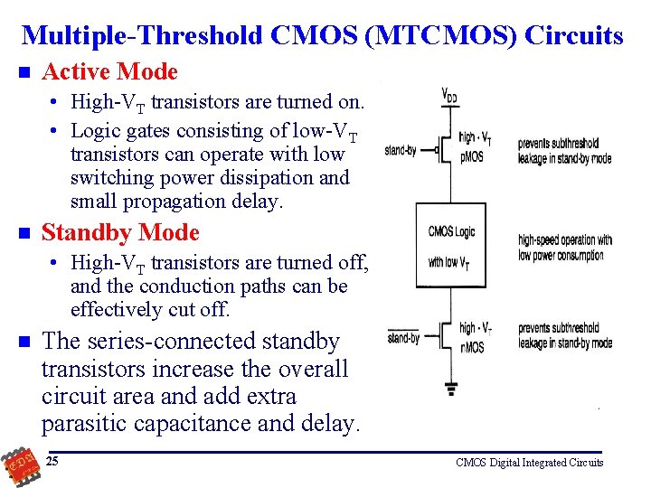
Multiple-Threshold CMOS (MTCMOS) Circuits n Active Mode • High-VT transistors are turned on. • Logic gates consisting of low-VT transistors can operate with low switching power dissipation and small propagation delay. n Standby Mode • High-VT transistors are turned off, and the conduction paths can be effectively cut off. n The series-connected standby transistors increase the overall circuit area and add extra parasitic capacitance and delay. 25 CMOS Digital Integrated Circuits

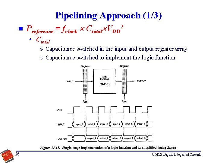
Pipelining Approach (1/3) n Preference = fclock Ctotal VDD² • Ctotal » Capacitance switched in the input and output register array » Capacitance switched to implement the logic function 26 CMOS Digital Integrated Circuits

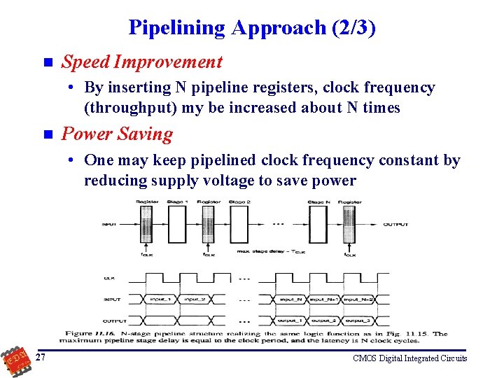
Pipelining Approach (2/3) n Speed Improvement • By inserting N pipeline registers, clock frequency (throughput) my be increased about N times n Power Saving • One may keep pipelined clock frequency constant by reducing supply voltage to save power 27 CMOS Digital Integrated Circuits

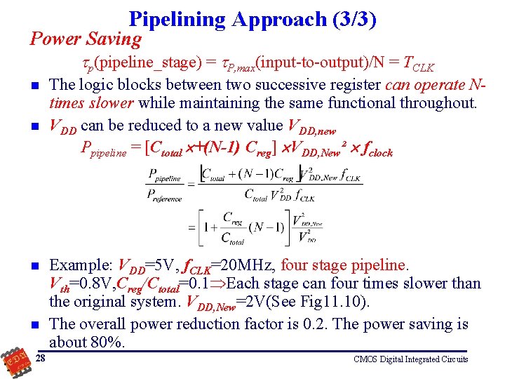
Pipelining Approach (3/3) Power Saving p(pipeline_stage) = P, max(input-to-output)/N = TCLK n n 28 The logic blocks between two successive register can operate Ntimes slower while maintaining the same functional throughout. VDD can be reduced to a new value VDD, new Ppipeline = [Ctotal +(N-1) Creg] VDD, New² fclock Example: VDD=5 V, f. CLK=20 MHz, four stage pipeline. Vth=0. 8 V, Creg/Ctotal=0. 1 Each stage can four times slower than the original system. VDD, New=2 V(See Fig 11. 10). The overall power reduction factor is 0. 2. The power saving is about 80%. CMOS Digital Integrated Circuits

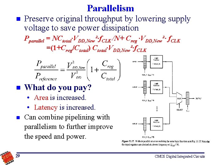
Parallelism n Preserve original throughput by lowering supply voltage to save power dissipation Pparallel = NCtotal·VDD, New²·f. CLK /N+ Creg ·VDD, New²· f. CLK =(1+Creg/Ctotal) Ctotal·VDD, New²·f. CLK n What do you pay? n • Area is increased. • Latency is increased. Can combine pipelining with parallelism to further improve the speed and power. 29 CMOS Digital Integrated Circuits

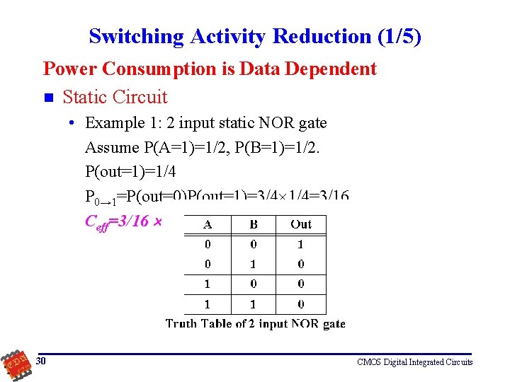
Switching Activity Reduction (1/5) Power Consumption is Data Dependent n Static Circuit • Example 1: 2 input static NOR gate Assume P(A=1)=1/2, P(B=1)=1/2. P(out=1)=1/4 P 0→ 1=P(out=0)P(out=1)=3/4 1/4=3/16 Ceff=3/16 CL 30 CMOS Digital Integrated Circuits

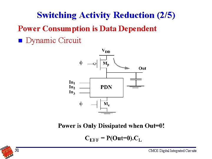
Switching Activity Reduction (2/5) Power Consumption is Data Dependent n Dynamic Circuit 31 CMOS Digital Integrated Circuits

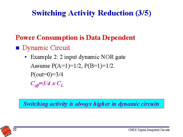
Switching Activity Reduction (3/5) Power Consumption is Data Dependent n Dynamic Circuit • Example 2: 2 input dynamic NOR gate Assume P(A=1)=1/2, P(B=1)=1/2. P(out=0)=3/4 Ceff=3/4 CL Switching activity is always higher in dynamic circuits 32 CMOS Digital Integrated Circuits

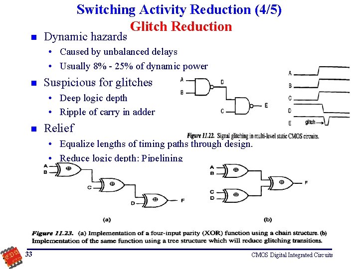
n Switching Activity Reduction (4/5) Glitch Reduction Dynamic hazards • Caused by unbalanced delays • Usually 8% - 25% of dynamic power n Suspicious for glitches • Deep logic depth • Ripple of carry in adder n Relief • Equalize lengths of timing paths through design. • Reduce logic depth: Pipelining 33 CMOS Digital Integrated Circuits

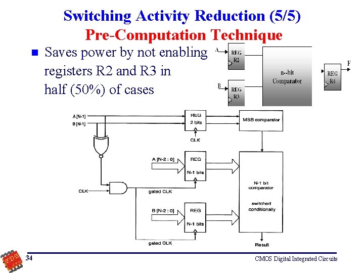
Switching Activity Reduction (5/5) Pre-Computation Technique n 34 Saves power by not enabling registers R 2 and R 3 in half (50%) of cases CMOS Digital Integrated Circuits

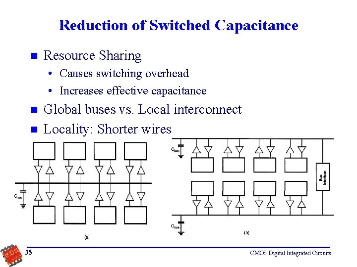
Reduction of Switched Capacitance n Resource Sharing • Causes switching overhead • Increases effective capacitance n n 35 Global buses vs. Local interconnect Locality: Shorter wires CMOS Digital Integrated Circuits

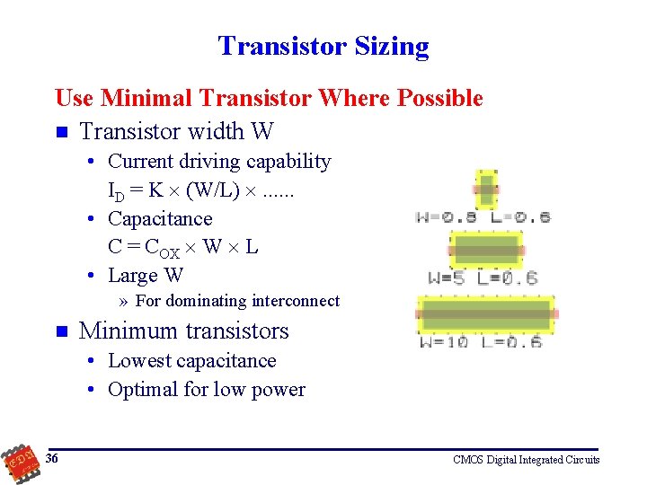
Transistor Sizing Use Minimal Transistor Where Possible n Transistor width W • Current driving capability ID = K (W/L) . . . • Capacitance C = COX W L • Large W » For dominating interconnect n Minimum transistors • Lowest capacitance • Optimal for low power 36 CMOS Digital Integrated Circuits

Design for Low Power (Cont. ) n Process Technology • VDD reduction • Threshold voltage » High threshold voltage » Double-threshold devices • Low threshold for high speed • High threshold for low power • Silicon on insulator (SOI) 37 CMOS Digital Integrated Circuits

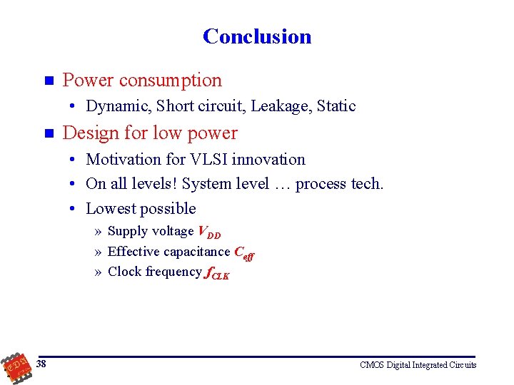
Conclusion n Power consumption • Dynamic, Short circuit, Leakage, Static n Design for low power • Motivation for VLSI innovation • On all levels! System level … process tech. • Lowest possible » Supply voltage VDD » Effective capacitance Ceff » Clock frequency f. CLK 38 CMOS Digital Integrated Circuits