Common mode feedback for fully differential amplifiers Differential

Common mode feedback for fully differential amplifiers

Differential amplifiers • Cancellation of common mode signals including clock feed-through • Cancellation of even-order harmonics • Double differential signal swing, SNR↑ 3 d. B Symbol:

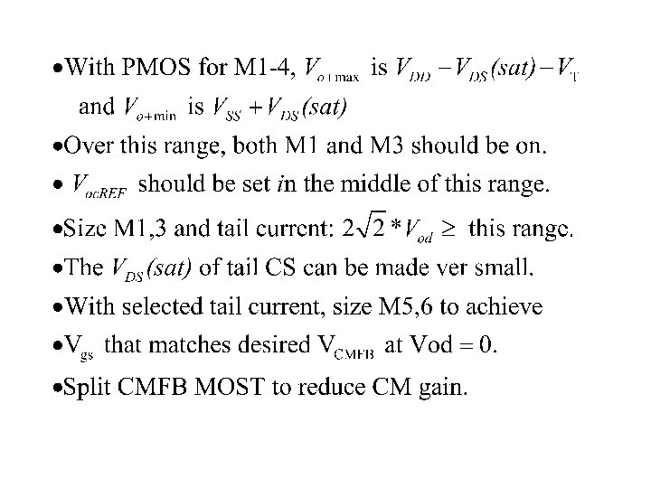
Two-Stage, Miller, Differential-In, Differential-Out Op Amp peak-to-peak output voltage 2·OCMR Output common mode range (OCMR) = VDD-VSS - VSDPsat - VDSNsat

Common Mode Output Voltage Stabilization Common mode drift at output causes differential signals move into triode region

Common Mode feedback • All fully differential amplifier needs CMFB • Common mode output, if uncontrolled, moves to either high or low end, causing triode operation • Ways of common mode stabilization: – external CMFB – internal CMFB

Common mode equivalent VBP Vo 1 cm Vicm VBN I 2 Vocm I 1

VBP I 1 I 2 Vo 1 cm Vicm Vo Vicm VBN What about single ended? Does it have the same problem? Does it require feedback stabilization?

VBP I 3 Yes, to all three questions I 4 Vo 1 cm Vi- I 1 VBN I 2 I 6 Vo Vi+ I 7 To match I 1 and I 3, the diode connection provides the single stage negative feedback to automatically generate Vg 3. The match between I 2 and I 4, and I 6 and I 7 is a two stage problem and requires negative feedback: needs feedback from Vo to Vi-.

All op amps must be used in feedback configuration! VBP I 3 I 4 Vo 1 cm Vi- I 1 I 2 I 3 I 4 Vo 1 cm Vi. I 1 VBN Vo I 7 VBN VBP Vi+ I 6 I 2 Vi+ I 6 Vo I 7 Buffer connection or resistive feedback provides the needed negative feedback

Fully differential amplifiers are also used in feedback configuration. Vi+ Vi- Vp Vn Hence, differential signal is well defined. Vo. Vo+

But when you add the first two equations Vi+ You get: Vi- Vp Vn Vo. Vo+ Since Vp+Vn is undefined, Vo++Vo- is undefined.

Basic concept of CMFB: Since diff feedback and diff input uses Vin+ and Vin-, CMFB has to be applied to somewhere else: like a bias current Vo+ +Vo- Vo+ CM Vo- Dvb 2 measurement CMFB Voc e Voc. Ref + desired common mode voltage

Basic concept of CMFB: Vo+ +Vo- Vo+ CM Vo- Dvb 2 measurement CMFB e Voc e Vo. CRef + Find transfer function from e to Voc: ACMF(s) Find transfer function from an error source to Voc: Aerr(s) Voc error due to error source: err*Aerr(0)/ACMF(0)

example HW: When Vb 2 changes by D, how much does Voc change? Vb 2 M 3 M 4 M 8 M 6 CC Vi+ M 1 VCMFB M 2 CC Vi- Vo+ M 5 Vo- Vb 1 VCMFB M 7 Voc ACMFB + M 9 - Vo+ 1/2 Vo- When Vic changes by D, how much does Voc change? What circuit design tricks can be used to reduce Voc change?

Example Voc ? ? Voc. Ref Need to make sure to have negative feedback

Resistive C. M. detectors: Vo+ R 1 R 2 Vo-

Resistive C. M. detectors: Vo. c. Vo+ Vi+ R 1 Vo- Vi- Not recommended. The resistive loading kills gain.

Buffer Vo+, Vo- before connecting to R 1. Voc Vo+ Vo. R 1 Simplementation: source follower Vo+ Vo. c. Vo- * Gate capacitance is added to your amp load.

Why not: Vo+ Voc Vo- Voc node is floating!! Solution: add leakage to drain Voc node. Vo+ Voc Vo-

Practical: Combine resistor, capacitor, and buffering VDD M 7 A 75/3 150/3 M 2 A 150/3 M 2 B BIAS 4 75/3 300/2. 25 BIAS 2 BIAS 1 M 3 A OUT+ M 1 A 20 K Source M 12 B M 12 A 1000/2. 25 follower M 1 B 200/2. 25 M 10 CL=4 p. F 200/2. 25 20 K 300/2. 25 IN+ M 11 150/2. 25 M 8 150/2. 25 M 13 B 300/2. 25 INM 6 AB 75/2. 25 M 13 A averager. OUT- M 3 B BIAS 3 75/2. 25 300/3 1. 5 p. F M 7 B M 6 C 300/3 4 p. F M 5 M 9 A 50/2. 25 M 9 B 50/2. 25 M 4 A 50/2. 25 M 4 B 50/2. 25 VSS Folded cascode amplifier

To increase or decrease the C. M. loop gain: e. g. Voc. Ref VCMFB
 simultaneously. M 1,")
Another implementation • Use triode transistors to provide isolation & z(s) simultaneously. M 1, M 2 in deep triode. VGS 1, VGS 2>>VT In that case, circuit above M 1, M 2 needs to ensure that M 1, M 2 are in triode. Voc Vo+ Vo. M 1 can be a c. s. M 2 I 1 = b((Vo+ – VT)Vx – 0. 5 Vx^2) I 2 = b((Vo- – VT)Vx – 0. 5 Vx^2) I = 2 b((Vo+ + Vo-)/2 – VT)Vx – 0. 5 Vx^2) =2 b((Voc – VT)Vx – 0. 5 Vx^2) Vx = Voc–VT – ((Voc–VT)^2 -I/b)^0. 5 d. Vx/d. Voc – Vx/(Voc – VT)

Example: Input stage Vo- Vb M 1 M 2 e. g. Vo+, Vo-≈2 V at Q & Vb ≈1 V , Then M 1&2 will be in deep triode. Vo+

Vo- Vo+ Vb 1 Vb 2 VX M 1 M 2

Two-Stage, Miller, Differential-In, Differential -Out Op Amp M 10 and M 11 are in deep triode

Vo++ Vo 2 Voc. REF. VCMFB Vo+ Vo- Note the difference from the book accommodates much larger Voc range

Small signal analysis of CMFB Example: IB M 3 Vout+ M 1 -Δi M 4 IB M 2 -Δi Vout- +Δi +Δi Voc. REF M 5 +Δi VCMFB Δi=0 2Δi VCMFB Differential signal Common mode signal -Δi

M 3 Voc. REF M 1 M 2 M 5 M 6 M 4

• Differential Vo: Vo+↓ by ΔVo, Vo-↑ by ΔVo • Common mode Vo: Vo+↑ by ΔVo, Vo-↑ by ΔVo

Switched cap CMFB supports full Vo swing: VSS to VDD Vo+ Φ 1 VCMFB Vo- Φ 2 Φ 1 Vo. CRef Vb-repl Vo. CRef During phi_1, the left cap are charged by the op amp output, and the right caps are charged by the reference and nominal bias voltage. During phi_2, the charges are averaged.

One simplified implementation VCM: desired Voc VGS 14: desired bias Split for gain reduction C 1=C 2

Points to consider • If supply is high: – S 2 can be NMOS – S 1 and S 3 can be either NMOS or PMOS or transmission gates – S 4 an S 5 must be transmission gates • If supply is very low: – May need to use charge pump to boost the switch gate voltages • Error due to charge injection from switches – Intentionally offset VCM and VGS 14 – Use simulation to determine the right values

Bandwidth of CMFB loop • Ideally, if CM and DM are fully decoupled, CM only needs to stabilize operating points. CM bandwidth only needs to be wide enough to handle disturbances affecting operating points. • Practically, there is CM DM conversion. CM loop needs to handle disturbances of bandwidth comparable to DM BW • But CM loop shares most of DM poles and have additional poles, difficult to achieve similar bandwidth, make CM loop bandwidth a few times lower than DM Here Bandwidth = unity loop gain frequency

Example VBP I 1 I 2 Vo 1 Vo Vi++Vicm VBN Vi-+Vicm VCMFB VBN

CM and DM equivalent circuit Comparison VBP CM Vo 1 cm Vocm VCMFB ro 1=rdsp||rcascode≈rdsp gm = ½gm 5 ½Vo 1 d I 2 Vid ½ M 5 DM VBN I 1 I 2 -½Vid ½Vod AC GND VBN I 1 ro 1=rdsp||rdsn≈ ½rdsp gm = gm 1 ØLow frequency pole p 1 is about 2 X lower in CM; ØDC gain is change by 2*½gm 5/gm 1, Øunity gain frequency gm/CC is changed by ½gm 5/gm 1, Øhigh frequency poles and zeros of DM remain in CM, ØCM has one additional node at D 5 similar or worse PM at unity gain fre

To ensure sufficient CMFB loop stability • CMFB loop gain = CM gain from VCMFB to Voc * gain of CMFB circuit • To ensure sufficient PM for CMFB loop – Make the DC gain of CMFB circuit to be a few time less than one – That makes the CMFB loop UGF to be a few times lower than DM gain’s UGF – Make sure the additional pole in the CM gain and any additional poles from the CMFB circuit to be at higher frequency than DM UGF

CM gain’s additional pole at D 5 is given by: ~ -gm 1/(Cgs 1+½Cdb 5) This is close to f. T of M 1. So at very high fre. If the CMFB circuit below is to be used, then the following needs to be true: 1. IB and M 5 sized to give desired VCMFB when Vo+=Vo-=desired 2. CMFB circuit DC gain ACMFB=2 gm 1 f/gm 5 f is small. 3. Pole of CMFB – gm 5 f/(Cgs 5+Cgs 5 f+Cdb 1, 2 f) >> ACMFB*(UGF of DM) VBP Vo+ M 1 f VCMRef IB M 3 f VBP M 4 f IB M 2 f Vo- Also, W/L of M 1 -4 f should be small, so that their VEB is large to accommodate Vo+, Vo- swing. This is consistent with (1. ) above VCMFB M 5 f

Also, W/L of M 1 -4 f should be small, so that their VEB is large to accommodate Vo+, Vo- swing. At Q-pt, Vo+, Vo- and VCMRef are all equal, and VS 1 f = VCMRef + VTP + VEB When Vo+ is at Vomax, M 1 f turns off and all current goes to M 3 f, M 3 f has 20. 5 VEB, M 1 f has 0 VEB. Hence, VS 1 f = VCMRef + VTP + 20. 5 VEB, and VS 1 f = Vomax = VCMRef + 20. 5 VEB. Similarly, VS 2 f = Vomin = VCMRef – 20. 5 VEB. Hence, Voswing = 2*20. 5*VEB >= Voswing /2*20. 5 But, IB need to be in saturation, hence VS 1 fmax = VCMRef + VTP + VEB <= VBP+VTP VCMRef <= VBP – Voswing /2*20. 5
 70 d. B")
Example DC gains 85 d. B 80 d. B Av. CM(w) 70 d. B But does not mean CM Q point can be maintained with 70 d. B accuracy! Av. DM(w) Av. CMFBLoop(w) w -15 d. B Av(w) of CMFB circuit

Why?

Because op amp is always used in feedback configuration. DM feedback also kills CM gain, since DM and CM share the same path from vo 1 to vo. VBP I 1 Vo 1 - I 2 Vi+ VBN Vo+ VCMFB Ri Rf VBN Rf Ri Vin+

VBP CM Vo 1 cm I 2 Vicm = -b. Vocm Vicm Vocm gm=gm 1/(1+2 gm 1 ro 5) VCMFB ½ M 5 VBN I 1 -1
 70 d. B")
Example DC gains 85 d. B 80 d. B Av. CM(w) 70 d. B New Av. CM(w) Av. DM(w) gm 5 ro 5/b 40 d. B 25 d. B Av. CMFBLoop(w) New Av. CMFBLoop(w) -15 d. B Av(w) of CMFB circuit w

Is it good enough to stabilize the CM Q points to -25 d. B accuracy level? If not, what can be done? Increase the effective gm 5 ro 5! That is: use cascode tail current source. This will improve the CMFB loop gain under DM feedback by about 30 to 35 d. B. Or, increase the gain of CMFB circuit. In doing so, avoid introducing high impedance node, avoid introducing poles near or lower than DM GB.

Voc variation range • Voc variation comes from two sources – Input common mode – Common mode PVT variations • Vicm induced Voc variation – Find closed-loop Vicm range – Find closed-loop gain from Vicm to Voc – Find contribution to Voc variation • PVT induced Voc variation – Refer all PVT variations to VBP variation – Find gain closed-loop from VBP to Voc – Find contribution to Voc variation

VBP CM Vo 1 cm I 2 Vicm V’icm Vocm -1 gm=gm 1/(1+2 gm 1 ro 5) VCMFB ½ M 5 VBN CMFB circuit I 1 Vocm-Des
- Slides: 47