Course Analog Circuit Design Time schedule Mo 11


 is Energetic State Density function in the material.")


")


")
 POLYSILICON RESISTORS • Lower coupling with substrate •")


")
")
")


=3. 8 COX ~")


Δx = A – P")

")
![INTEGRATED CAPACITORS: LAYOUT 3 Matching: capacitors with not-integer ratio [C 2/C 1] -1 squared](https://slidetodoc.com/presentation_image_h/e816f4d35cc4f15242518d00c087c5a0/image-52.jpg "INTEGRATED CAPACITORS: LAYOUT 3 Matching: capacitors with not-integer ratio [C 2/C 1] -1 squared")

- Slides: 53
Course: Analog Circuit Design Time schedule: Mo 11. 00 -13. 00 We 11. 00 -13. 00 Th 14. 00 -16. 00 Office hours: Mo 16. 00 -18. 00 Exams: Feb. (2), Jun. -Jul. (2), Sep. (2) Oral examination Additional course material: ftp: //ftp. dii. unisi. it/pub/users/vignoli/Analog_Circuit_Design Please, register at the following link: goo. gl/k. JXGzy
Course: Analog Circuit Design Time schedule: Mo 11. 00 -13. 00 11. 30 -13. 00 We 11. 00 -13. 00 11. 30 -13. 00 Th 14. 00 -16. 00 14. 30 -16. 00 Office hours: Mo 16. 00 -18. 00 Exams: Feb. (2), Jun. -Jul. (2), Sep. (2) Oral examination Additional course material: ftp: //ftp. dii. unisi. it/pub/users/vignoli/Analog_Circuit_Design Please, register at the following link: goo. gl/k. JXGzy
References: F. Maloberti Analog Design for CMOS VLSI Systems Kluwer 2001 J. Millman, C. Halkias Integrated Electronics: Analog and Digital Circuit and Systems Mc. Graw-Hill 1972 A. Sedra, K. Smith Microelectronic Circuits (7 th edition) Oxford University Press 2014 P. Gray, R Meyer Analysis and Design of Analog Integrated Circuits (3 rd ed. ) Wiley 1993 M. S. Tyagi Introduction to Semiconductor Material and Devices Wiley 1991
MATERIALS: electric behavior semiconductor Insulator conductor
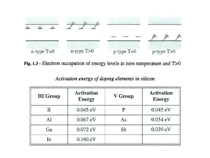
SEMICONDUCTORS: electric behavior Fermi-Dirac distribution: occupation probability for the energy level E In semiconductors EF is in the Band-Gap
Intrinsic Semiconductors: free carriers where Ne(E) is Energetic State Density function in the material. NC is the number of available states (per cm-3) in the conduction band
DOPING ACCEPTOR DONOR EF n-type The Fermi energy moves with doping T effect EF p-type
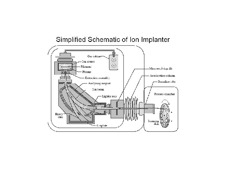
PHOTOLITOGRAPHY Photoresist spin. -coating EXPOSITION: The mask is transferred to the photoresist Thick film: 1 mm Uv - X-ray
• The photoresist chemically reacts and dissolves in the developing solution, only on the parts that were not masked during exposure (positive method). • Development is performed with an alkaline developing solution. • After the development, photoresist is left on the wafer surface in the shape of the mask pattern. Masked photoresist solvents remove exposed (unexposed) resist Etching removes material from wafer surface where resist has been removed
Dry etching Wet etching
Also PVD
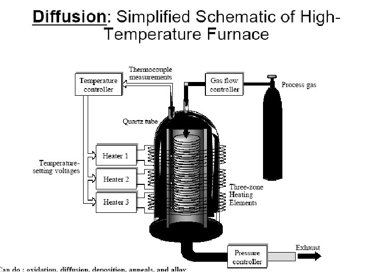
Materials: Si substrate • Monocrystalline silicon is produced from purified polycrystalline silicon by “pulling” an ingot – polysilicon is melted using radio frequency induction heaters – “seed crystal” of monocrystalline silicon is dipped into melt – silicon grows around structure of seed as seed is slowly withdrawn • Sawed into wafers about 600 microns thick – only a few microns are actually used for IC devices – then etched, polished, and cleaned – stacked in carriers
Materials • Single crystal silicon – SCS – Anisotropic crystal – Semiconductor, great heat conductor • Silicon dioxide is created by interaction between silicon and oxygen or water vapor – – Si + O 2 = Si. O 2 or Si + 2 H 2 O = Si. O 2 + 2 H 2 Excellent thermal and electrical insulator protects surface from contaminants forms insulating layer between conductors – forms barrier to dopants during diffusion or ion implantation – grows above and into silicon surface – Thermal oxide, LTO, PSG: different names for different deposition conditions and methods • Polycrystalline silicon – polysilicon – – – Mostly isotropic material Semiconductor also a conductor, but with much more resistance than metal or diffused layers created when silicon is epitaxially grown on Si. O 2 commonly used (heavily doped) for gate connections in most MOS processes • Silicon nitride – Si 3 N 4 – Excellent electrical insulator • Aluminum – Al – Metal – excellent thermal and electrical conductor
EFFECT OF FLATBAND VOLTAGE VFB (VFB < 0)
VGB = 0
SUBSTRATE P-type Si OXIDE Si. O 2 GATE Polisilicon SUBSTRATE CONTACT Polisilicon VGB VOX -VFB - - + Space charge regions -t. OX 0 x. D x Potential VGB-VFB VOX Φs(0) -t. OX x
STRONG INVERSION CONDITION
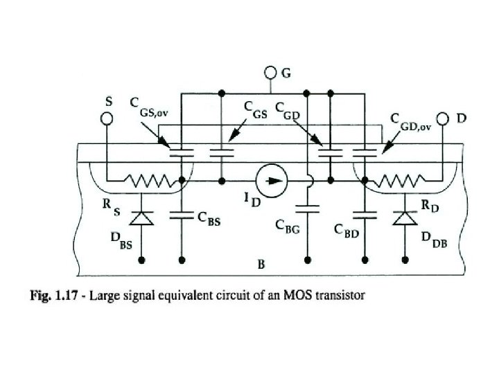
SMALL SIGNAL EQUIVALENT CIRCUIT OF A MOS TRANSISTOR
MOS TRANSISTOR LAYOUT • SOURCE AND DRAIN PARASITIC RESISTANCES • SOURCE AND DRAIN PARASITIC CAPACITANCES • MATCHING
SOURCE AND DRAIN PARASITIC RESISTANCES
SOURCE AND DRAIN PARASITIC CAPACITANCES
MATCHING You must avoid: D Use always the same MOS orientation in your layout: silicon is anisotropic S S D
MATCHING 1 2 3
MATCHING 1 2 3
MATCHING
DESIGN RULES Geometrical recommendations due to the limited accuracy of the technology (mask alignment, lateral diffusion, etching undercut, optical resolution…) Design Kit: design rules + Spice models and technology features
INTEGRATED RESISTORS 1
INTEGRATED RESISTORS 2 DIFFERENT SOLUTIONS (a)
INTEGRATED RESISTORS 3 DIFFERENT SOLUTIONS (b) POLYSILICON RESISTORS • Lower coupling with substrate • Up to two shieldings • Top shielding (from noisy metal lines, package coupling…. )
INTEGRATED RESISTORS 3
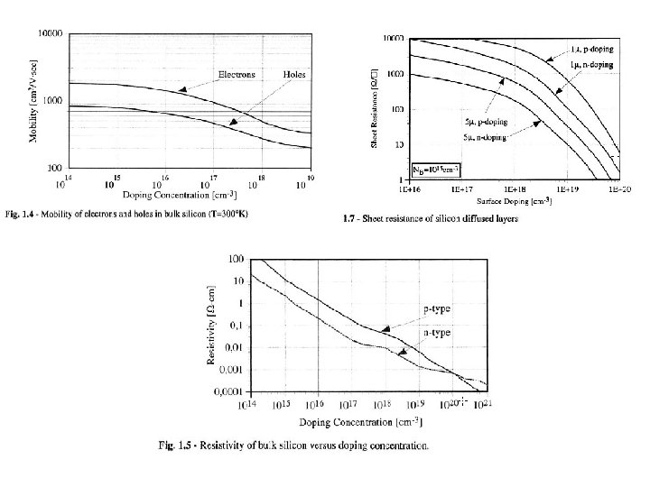
INTEGRATED RESISTORS 4 FACTORS AFFECTING ACCURACY • Poor absolute accuracy (20 -40% - large parameter drift) • Good matching (ratio) accuracy (0. 1 -0. 2% - it depends on local parameter variations)
INTEGRATED RESISTORS 5 Design Guidelines (a)
INTEGRATED RESISTORS 6 Design Guidelines (b)
INTEGRATED RESISTORS 7 Design Guidelines (c)
INTEGRATED CAPACITORS 1
INTEGRATED CAPACITORS 2
INTEGRATED CAPACITORS 3 COX tox ≤ 10 nm εr(Si. O 2)=3. 8 COX ~ 3. 36 f. F/μm 2
INTEGRATED CAPACITORS 4
INTEGRATED CAPACITORS 5
INTEGRATED CAPACITORS 6 A’ = W’L’ WL – 2 (L+W)Δx = A – P Δx = A (1 - Δx P/A) • The relative reduction of A remains constant, given Δx, if the ratio P/A is constant (matched elements) • The fringe effect reduces the capacitance at the plate boundary proportionally to tox P/A -> (L, W >> tox) • Effect of the thick oxides at the plate boundary
INTEGRATED CAPACITORS: LAYOUT 1 Layout examples for poly 1 -poly 2 capacitors
INTEGRATED CAPACITORS: LAYOUT 2 Matching: capacitors with integer ratio Shielding (well)
INTEGRATED CAPACITORS: LAYOUT 3 Matching: capacitors with not-integer ratio [C 2/C 1] -1 squared capacitors with area C 1 = L 2 1 rectangular capacitor with area [C 2/C 1] 1) C 1 Ck= Wk Lk = (C 2/C 1 - + All the capacitors with constant P/A L 2/4 L=L/4=Lk. Wk/2(Lk + Wk) Ck/C 1=Lk. Wk/L 2
PASSIVE COMPONENTS: CAPACITORS – Design Guidelines