Microelectronics Circuit Analysis and Design Donald A Neamen
- Slides: 64

Microelectronics Circuit Analysis and Design Donald A. Neamen Chapter 1 Semiconductor Materials and Devices Neamen Microelectronics, 4 e Mc. Graw-Hill Chapter 1 -1

In this chapter, we will: q Gain a basic understanding of semiconductor material properties Ø Two types of charged carriers that exist in a semiconductor Ø Two mechanisms that generate currents in a semiconductor q Determine the properties of a pn junction Ø Ideal current–voltage characteristics of a pn junction diode q Examine dc analysis techniques for diode circuits using various models to describe the nonlinear diode characteristics q Develop an equivalent circuit for a diode that is used when a small, time-varying signal is applied to a diode circuit q Gain an understanding of the properties and characteristics of a few specialized diodes q Design a simple electronic thermometer using the temperature characteristics of a diode Neamen Microelectronics, 4 e Mc. Graw-Hill Chapter 1 -2

Intrinsic Semiconductors q Ideally 100% pure material Ø Elemental semiconductors § Silicon (Si) • Most common semiconductor used today § Germanium (Ge) • First semiconductor used in p-n diodes Ø Compound semiconductors § Gallium Arsenide (Ga. As) Neamen Microelectronics, 4 e Mc. Graw-Hill Chapter 1 -3

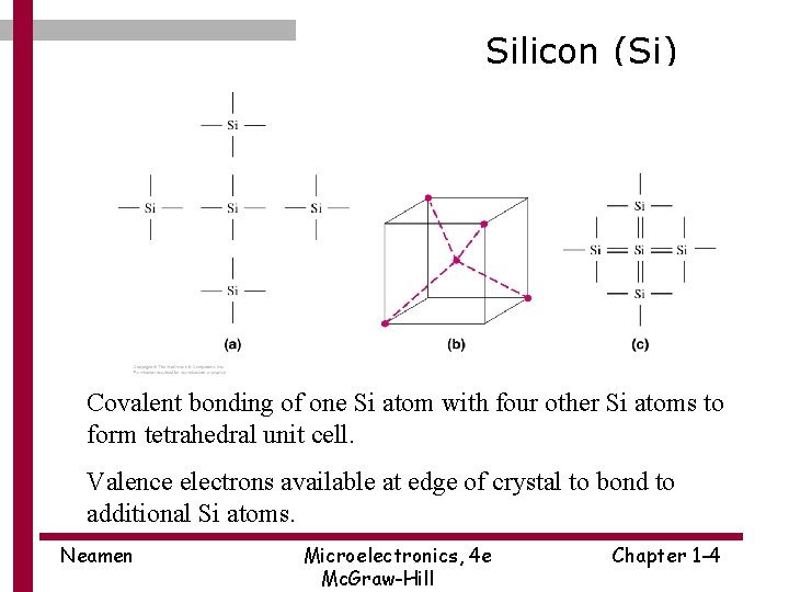
Silicon (Si) Covalent bonding of one Si atom with four other Si atoms to form tetrahedral unit cell. Valence electrons available at edge of crystal to bond to additional Si atoms. Neamen Microelectronics, 4 e Mc. Graw-Hill Chapter 1 -4

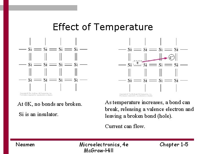
Effect of Temperature At 0 K, no bonds are broken. Si is an insulator. As temperature increases, a bond can break, releasing a valence electron and leaving a broken bond (hole). Current can flow. Neamen Microelectronics, 4 e Mc. Graw-Hill Chapter 1 -5

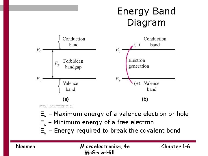
Energy Band Diagram Ev – Maximum energy of a valence electron or hole Ec – Minimum energy of a free electron Eg – Energy required to break the covalent bond Neamen Microelectronics, 4 e Mc. Graw-Hill Chapter 1 -6

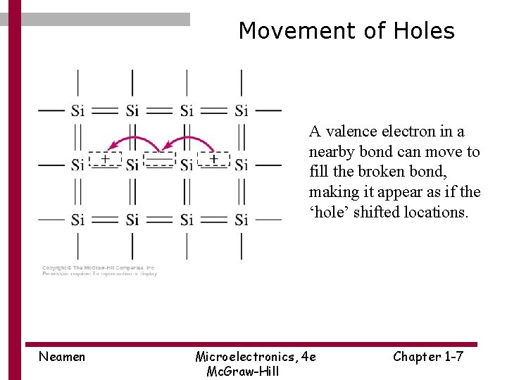
Movement of Holes A valence electron in a nearby bond can move to fill the broken bond, making it appear as if the ‘hole’ shifted locations. Neamen Microelectronics, 4 e Mc. Graw-Hill Chapter 1 -7

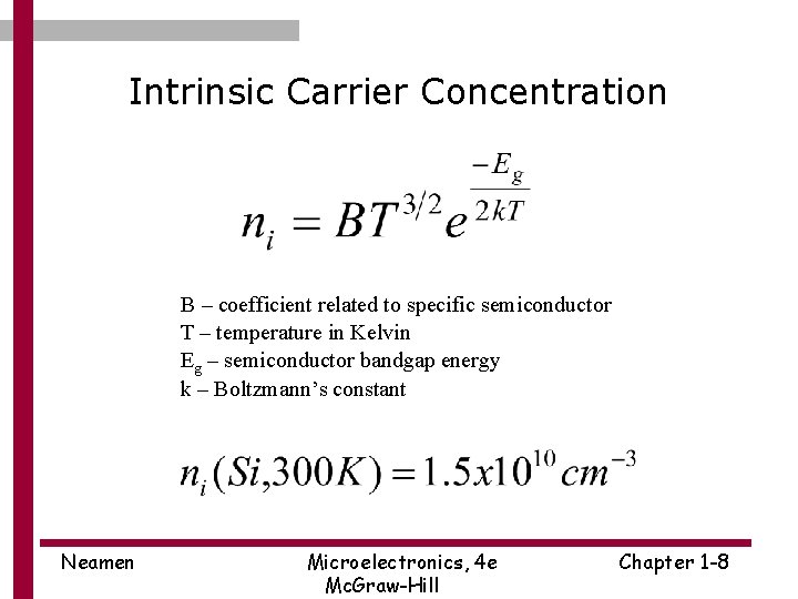
Intrinsic Carrier Concentration B – coefficient related to specific semiconductor T – temperature in Kelvin Eg – semiconductor bandgap energy k – Boltzmann’s constant Neamen Microelectronics, 4 e Mc. Graw-Hill Chapter 1 -8

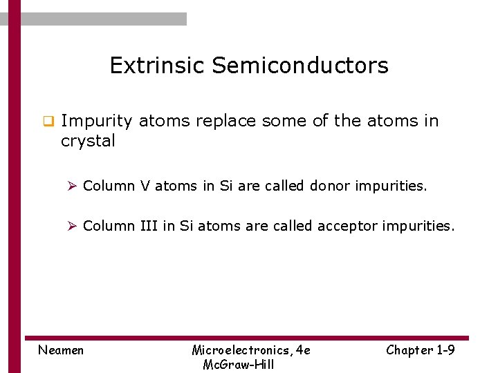
Extrinsic Semiconductors q Impurity atoms replace some of the atoms in crystal Ø Column V atoms in Si are called donor impurities. Ø Column III in Si atoms are called acceptor impurities. Neamen Microelectronics, 4 e Mc. Graw-Hill Chapter 1 -9

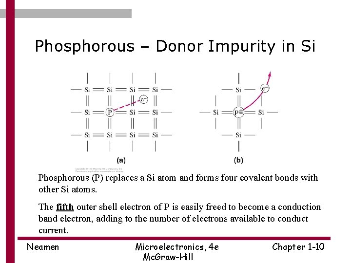
Phosphorous – Donor Impurity in Si Phosphorous (P) replaces a Si atom and forms four covalent bonds with other Si atoms. The fifth outer shell electron of P is easily freed to become a conduction band electron, adding to the number of electrons available to conduct current. Neamen Microelectronics, 4 e Mc. Graw-Hill Chapter 1 -10

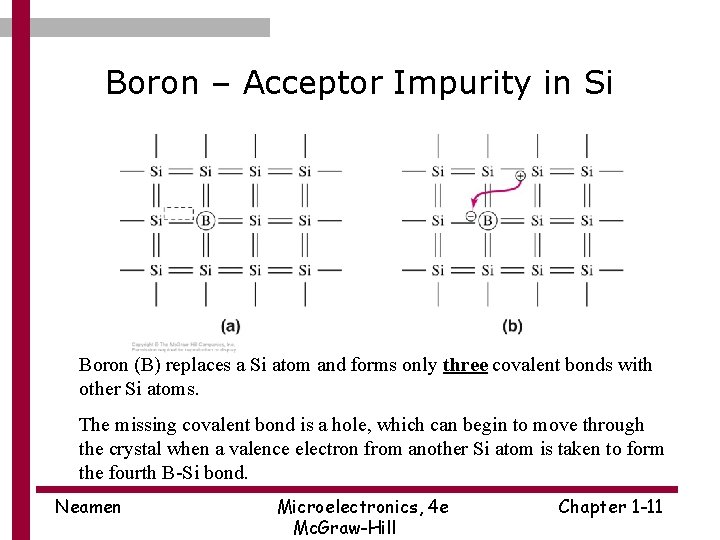
Boron – Acceptor Impurity in Si Boron (B) replaces a Si atom and forms only three covalent bonds with other Si atoms. The missing covalent bond is a hole, which can begin to move through the crystal when a valence electron from another Si atom is taken to form the fourth B-Si bond. Neamen Microelectronics, 4 e Mc. Graw-Hill Chapter 1 -11

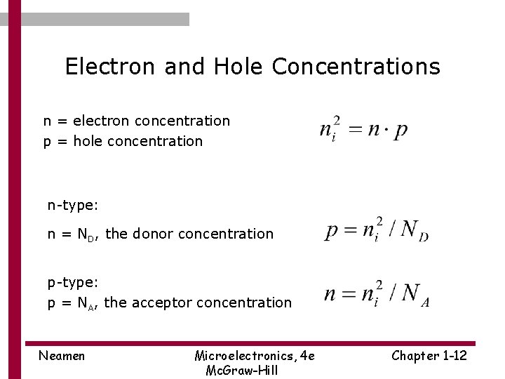
Electron and Hole Concentrations n = electron concentration p = hole concentration n-type: n = ND, the donor concentration p-type: p = NA, the acceptor concentration Neamen Microelectronics, 4 e Mc. Graw-Hill Chapter 1 -12

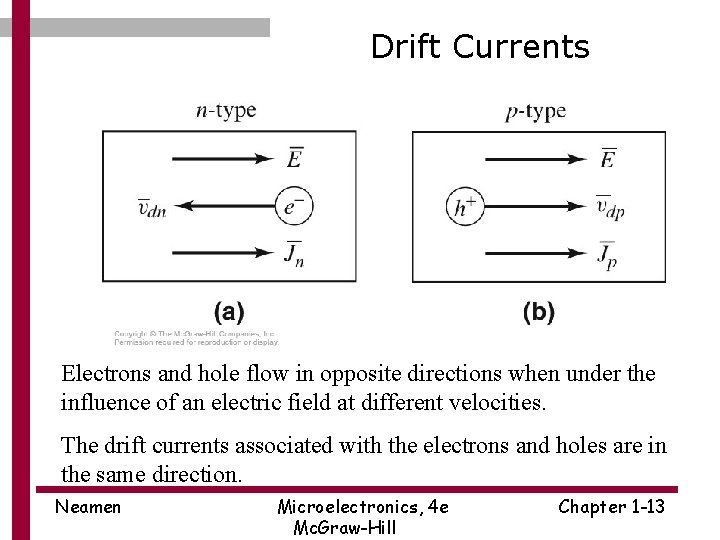
Drift Currents Electrons and hole flow in opposite directions when under the influence of an electric field at different velocities. The drift currents associated with the electrons and holes are in the same direction. Neamen Microelectronics, 4 e Mc. Graw-Hill Chapter 1 -13

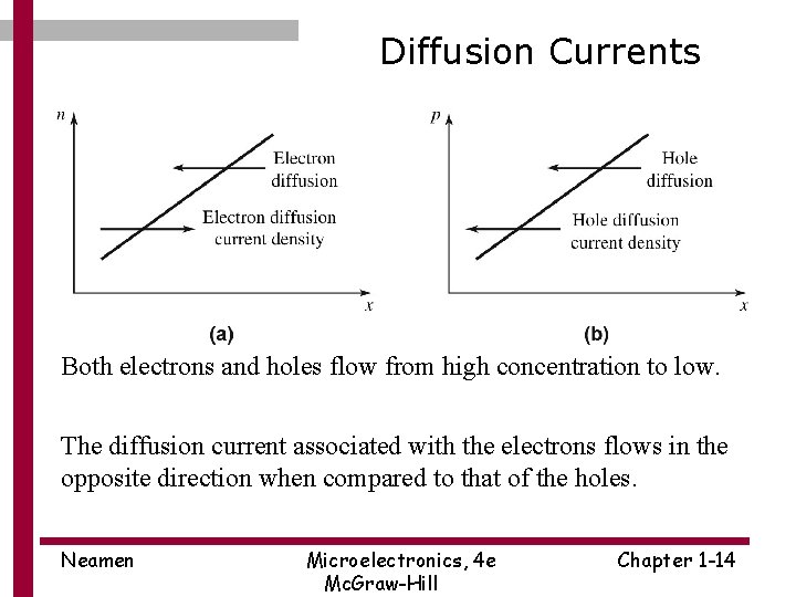
Diffusion Currents Both electrons and holes flow from high concentration to low. The diffusion current associated with the electrons flows in the opposite direction when compared to that of the holes. Neamen Microelectronics, 4 e Mc. Graw-Hill Chapter 1 -14

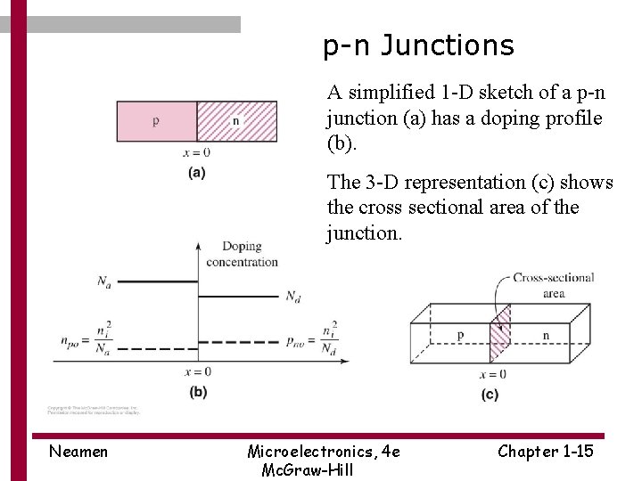
p-n Junctions A simplified 1 -D sketch of a p-n junction (a) has a doping profile (b). The 3 -D representation (c) shows the cross sectional area of the junction. Neamen Microelectronics, 4 e Mc. Graw-Hill Chapter 1 -15

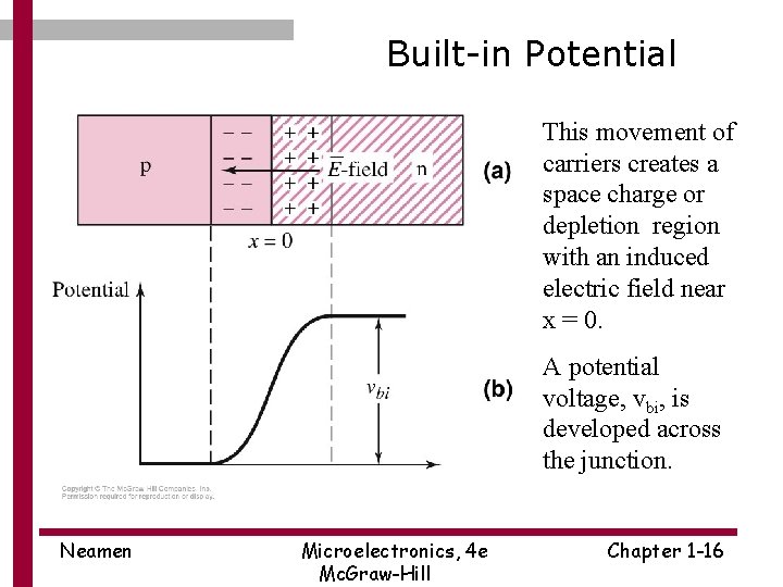
Built-in Potential This movement of carriers creates a space charge or depletion region with an induced electric field near x = 0. A potential voltage, vbi, is developed across the junction. Neamen Microelectronics, 4 e Mc. Graw-Hill Chapter 1 -16

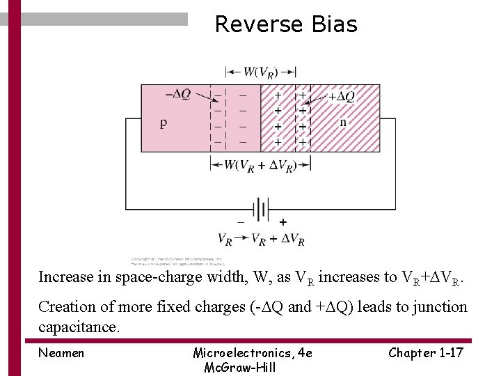
Reverse Bias Increase in space-charge width, W, as VR increases to VR+DVR. Creation of more fixed charges (-DQ and +DQ) leads to junction capacitance. Neamen Microelectronics, 4 e Mc. Graw-Hill Chapter 1 -17

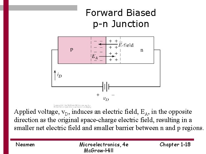
Forward Biased p-n Junction Applied voltage, v. D, induces an electric field, EA, in the opposite direction as the original space-charge electric field, resulting in a smaller net electric field and smaller barrier between n and p regions. Neamen Microelectronics, 4 e Mc. Graw-Hill Chapter 1 -18

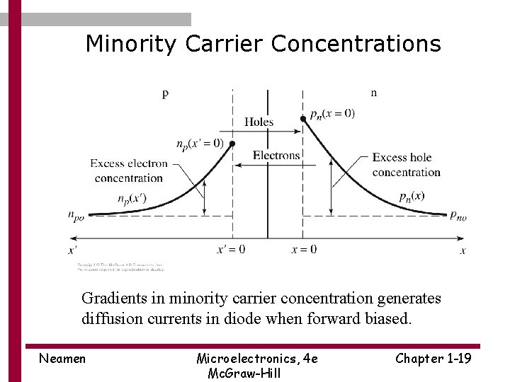
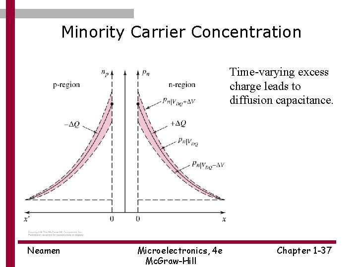
Minority Carrier Concentrations Gradients in minority carrier concentration generates diffusion currents in diode when forward biased. Neamen Microelectronics, 4 e Mc. Graw-Hill Chapter 1 -19

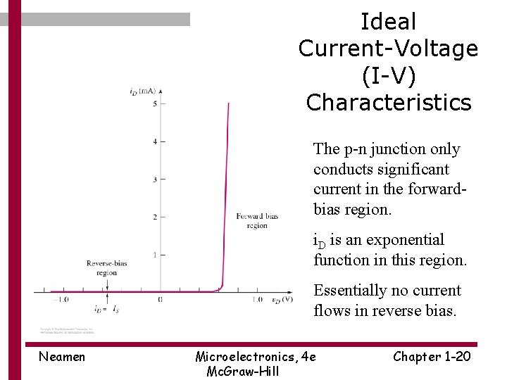
Ideal Current-Voltage (I-V) Characteristics The p-n junction only conducts significant current in the forwardbias region. i. D is an exponential function in this region. Essentially no current flows in reverse bias. Neamen Microelectronics, 4 e Mc. Graw-Hill Chapter 1 -20

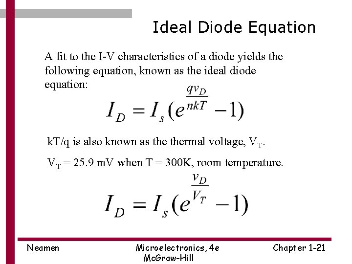
Ideal Diode Equation A fit to the I-V characteristics of a diode yields the following equation, known as the ideal diode equation: k. T/q is also known as thermal voltage, VT. VT = 25. 9 m. V when T = 300 K, room temperature. Neamen Microelectronics, 4 e Mc. Graw-Hill Chapter 1 -21

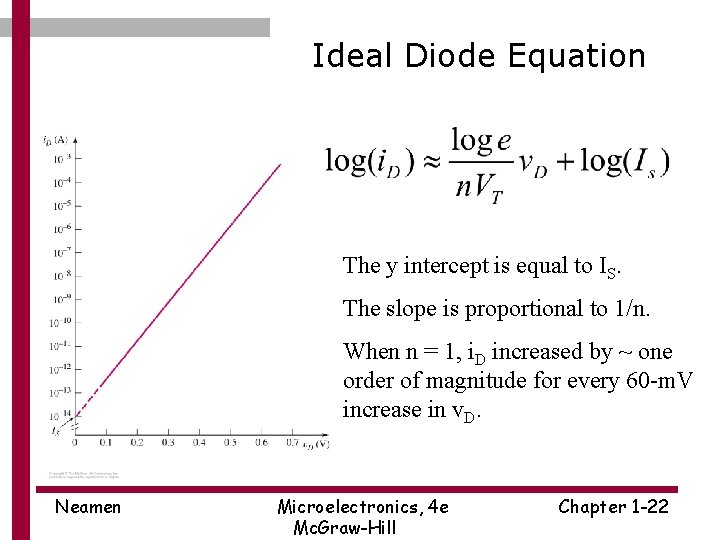
Ideal Diode Equation The y intercept is equal to IS. The slope is proportional to 1/n. When n = 1, i. D increased by ~ one order of magnitude for every 60 -m. V increase in v. D. Neamen Microelectronics, 4 e Mc. Graw-Hill Chapter 1 -22

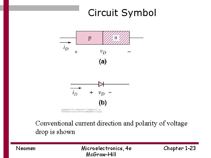
Circuit Symbol Conventional current direction and polarity of voltage drop is shown Neamen Microelectronics, 4 e Mc. Graw-Hill Chapter 1 -23

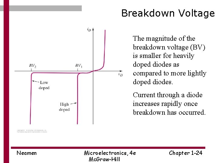
Breakdown Voltage The magnitude of the breakdown voltage (BV) is smaller for heavily doped diodes as compared to more lightly doped diodes. Current through a diode increases rapidly once breakdown has occurred. Neamen Microelectronics, 4 e Mc. Graw-Hill Chapter 1 -24

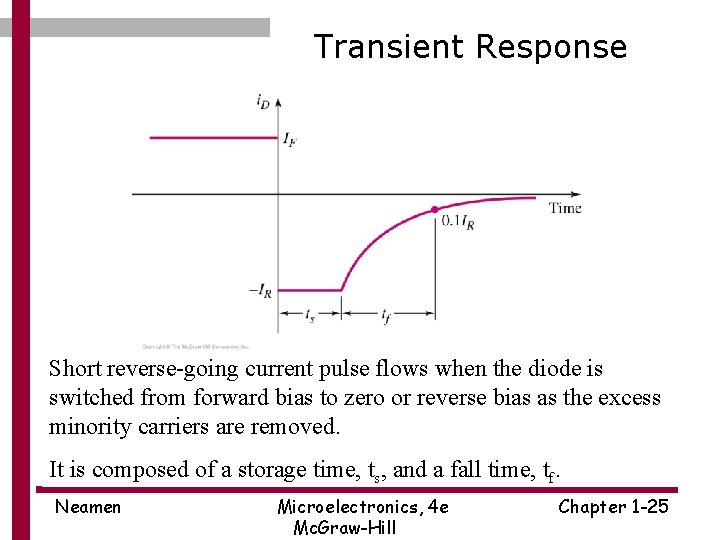
Transient Response Short reverse-going current pulse flows when the diode is switched from forward bias to zero or reverse bias as the excess minority carriers are removed. It is composed of a storage time, ts, and a fall time, tf. Neamen Microelectronics, 4 e Mc. Graw-Hill Chapter 1 -25

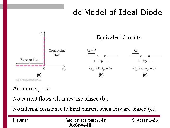
dc Model of Ideal Diode Equivalent Circuits Assumes vbi = 0. No current flows when reverse biased (b). No internal resistance to limit current when forward biased (c). Neamen Microelectronics, 4 e Mc. Graw-Hill Chapter 1 -26

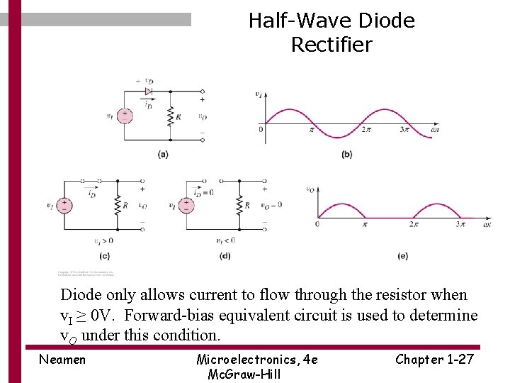
Half-Wave Diode Rectifier Diode only allows current to flow through the resistor when v. I ≥ 0 V. Forward-bias equivalent circuit is used to determine v. O under this condition. Neamen Microelectronics, 4 e Mc. Graw-Hill Chapter 1 -27

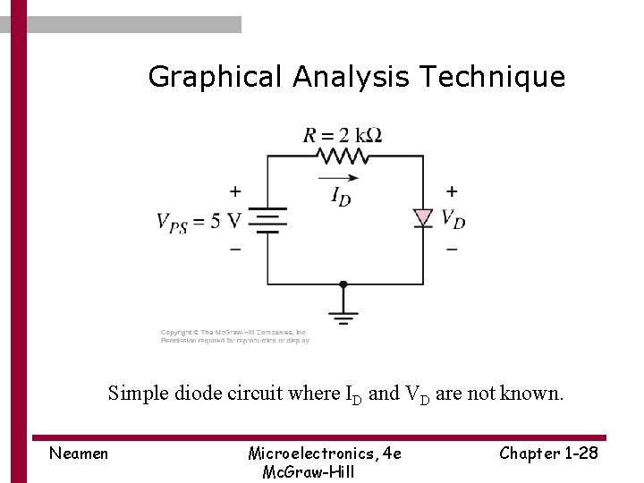
Graphical Analysis Technique Simple diode circuit where ID and VD are not known. Neamen Microelectronics, 4 e Mc. Graw-Hill Chapter 1 -28

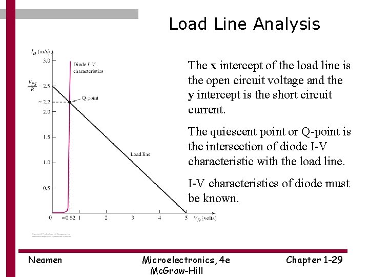
Load Line Analysis The x intercept of the load line is the open circuit voltage and the y intercept is the short circuit current. The quiescent point or Q-point is the intersection of diode I-V characteristic with the load line. I-V characteristics of diode must be known. Neamen Microelectronics, 4 e Mc. Graw-Hill Chapter 1 -29

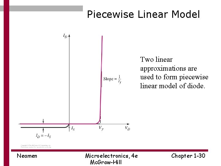
Piecewise Linear Model Two linear approximations are used to form piecewise linear model of diode. Neamen Microelectronics, 4 e Mc. Graw-Hill Chapter 1 -30

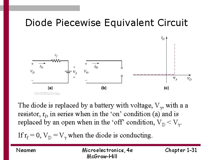
Diode Piecewise Equivalent Circuit The diode is replaced by a battery with voltage, Vg, with a a resistor, rf, in series when in the ‘on’ condition (a) and is replaced by an open when in the ‘off’ condition, VD < Vg. If rf = 0, VD = Vg when the diode is conducting. Neamen Microelectronics, 4 e Mc. Graw-Hill Chapter 1 -31

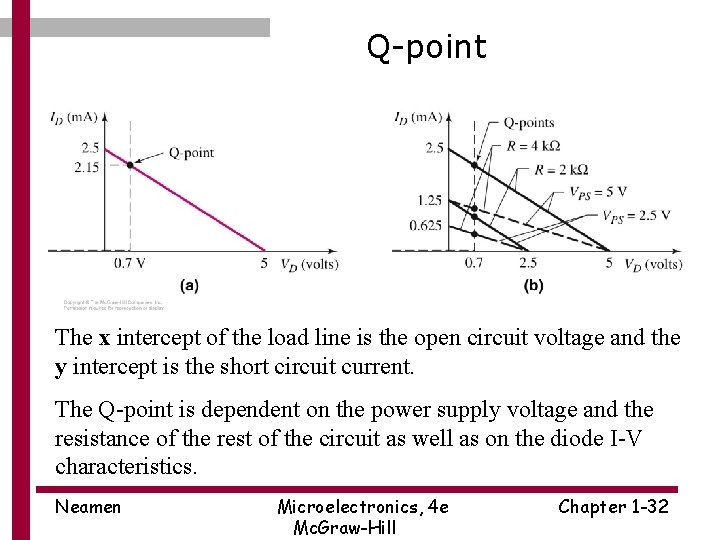
Q-point The x intercept of the load line is the open circuit voltage and the y intercept is the short circuit current. The Q-point is dependent on the power supply voltage and the resistance of the rest of the circuit as well as on the diode I-V characteristics. Neamen Microelectronics, 4 e Mc. Graw-Hill Chapter 1 -32

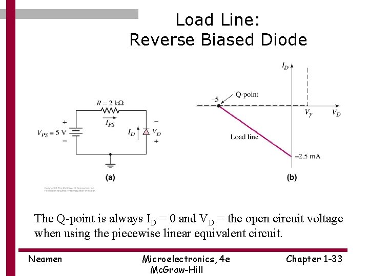
Load Line: Reverse Biased Diode The Q-point is always ID = 0 and VD = the open circuit voltage when using the piecewise linear equivalent circuit. Neamen Microelectronics, 4 e Mc. Graw-Hill Chapter 1 -33

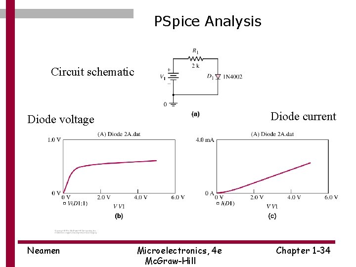
PSpice Analysis Circuit schematic Diode current Diode voltage Neamen Microelectronics, 4 e Mc. Graw-Hill Chapter 1 -34

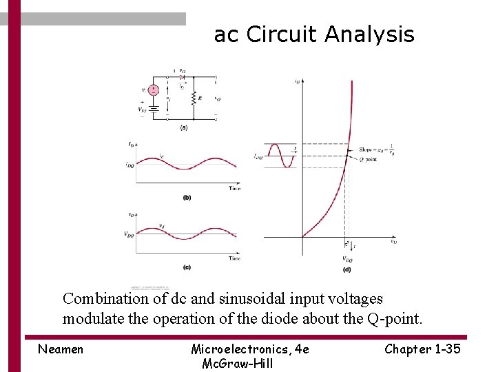
ac Circuit Analysis Combination of dc and sinusoidal input voltages modulate the operation of the diode about the Q-point. Neamen Microelectronics, 4 e Mc. Graw-Hill Chapter 1 -35

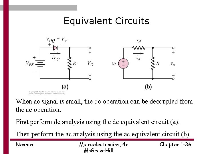
Equivalent Circuits When ac signal is small, the dc operation can be decoupled from the ac operation. First perform dc analysis using the dc equivalent circuit (a). Then perform the ac analysis using the ac equivalent circuit (b). Neamen Microelectronics, 4 e Mc. Graw-Hill Chapter 1 -36

Minority Carrier Concentration Time-varying excess charge leads to diffusion capacitance. Neamen Microelectronics, 4 e Mc. Graw-Hill Chapter 1 -37

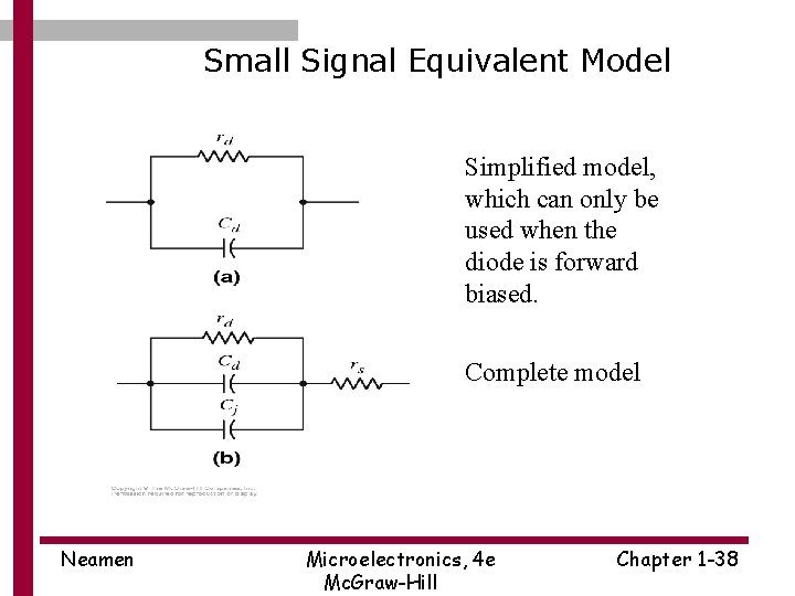
Small Signal Equivalent Model Simplified model, which can only be used when the diode is forward biased. Complete model Neamen Microelectronics, 4 e Mc. Graw-Hill Chapter 1 -38

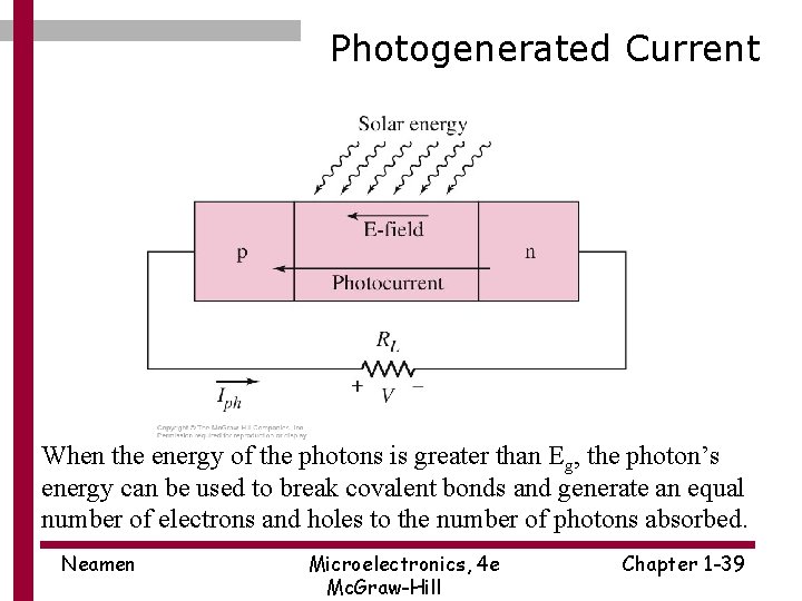
Photogenerated Current When the energy of the photons is greater than Eg, the photon’s energy can be used to break covalent bonds and generate an equal number of electrons and holes to the number of photons absorbed. Neamen Microelectronics, 4 e Mc. Graw-Hill Chapter 1 -39

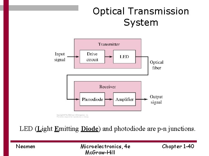
Optical Transmission System LED (Light Emitting Diode) and photodiode are p-n junctions. Neamen Microelectronics, 4 e Mc. Graw-Hill Chapter 1 -40

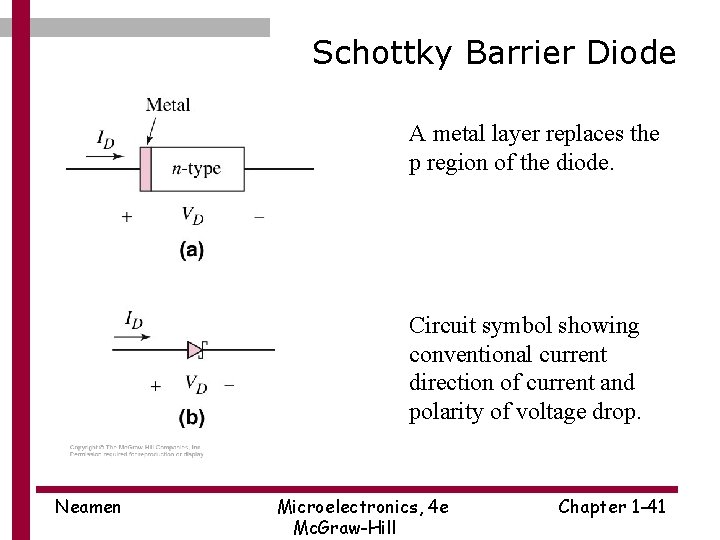
Schottky Barrier Diode A metal layer replaces the p region of the diode. Circuit symbol showing conventional current direction of current and polarity of voltage drop. Neamen Microelectronics, 4 e Mc. Graw-Hill Chapter 1 -41

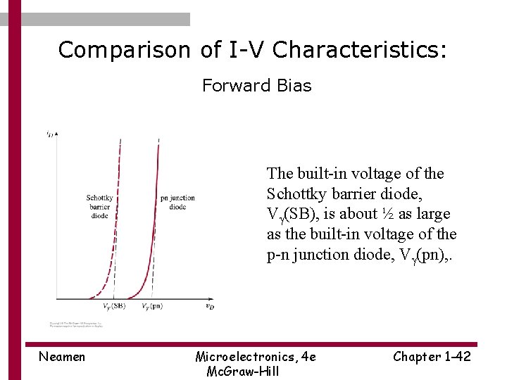
Comparison of I-V Characteristics: Forward Bias The built-in voltage of the Schottky barrier diode, Vg(SB), is about ½ as large as the built-in voltage of the p-n junction diode, Vg(pn), . Neamen Microelectronics, 4 e Mc. Graw-Hill Chapter 1 -42

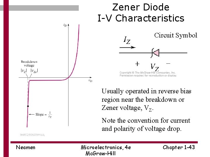
Zener Diode I-V Characteristics Circuit Symbol Usually operated in reverse bias region near the breakdown or Zener voltage, VZ. Note the convention for current and polarity of voltage drop. Neamen Microelectronics, 4 e Mc. Graw-Hill Chapter 1 -43

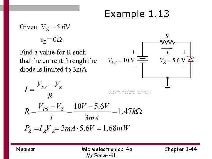
Example 1. 13 Given VZ = 5. 6 V r. Z = 0 W Find a value for R such that the current through the diode is limited to 3 m. A Neamen Microelectronics, 4 e Mc. Graw-Hill Chapter 1 -44

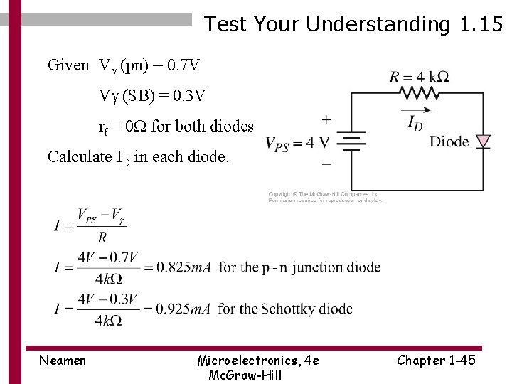
Test Your Understanding 1. 15 Given Vg (pn) = 0. 7 V Vg (SB) = 0. 3 V rf = 0 W for both diodes Calculate ID in each diode. Neamen Microelectronics, 4 e Mc. Graw-Hill Chapter 1 -45

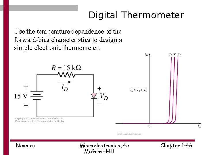
Digital Thermometer Use the temperature dependence of the forward-bias characteristics to design a simple electronic thermometer. Neamen Microelectronics, 4 e Mc. Graw-Hill Chapter 1 -46

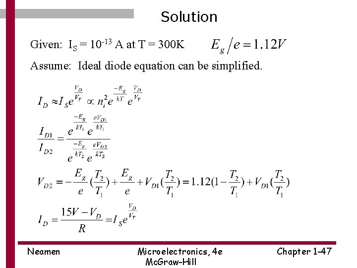
Solution Given: IS = 10 -13 A at T = 300 K Assume: Ideal diode equation can be simplified. Neamen Microelectronics, 4 e Mc. Graw-Hill Chapter 1 -47

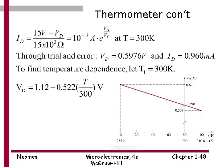
Thermometer con’t Neamen Microelectronics, 4 e Mc. Graw-Hill Chapter 1 -48

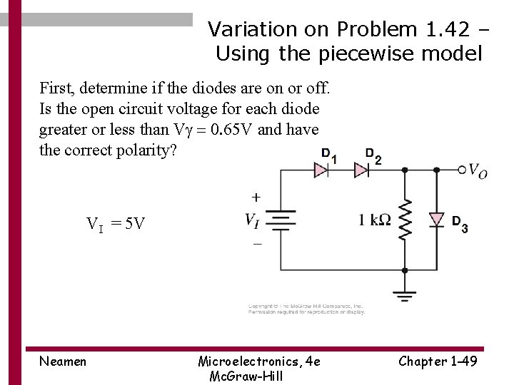
Variation on Problem 1. 42 – Using the piecewise model First, determine if the diodes are on or off. Is the open circuit voltage for each diode greater or less than Vg = 0. 65 V and have the correct polarity? VI = 5 V Neamen Microelectronics, 4 e Mc. Graw-Hill Chapter 1 -49

Variation con’t a) Test what would happen if D 3 was not conducting: If there enough voltage available to turn on D 1 and D 2? The power supply is +5 V and is attached on the p side of D 1. The n side of D 1 is attached to the p side of D 2. So, there is sufficient voltage and with the correct polarity from the power supply to turn on both diodes. A check to verify that both diodes are conducting – the open circuit voltage for each diode is equal to 5 V, which means that the load line will intersect the conducting section of the diode’s piecewise model Neamen Microelectronics, 4 e Mc. Graw-Hill Chapter 1 -50

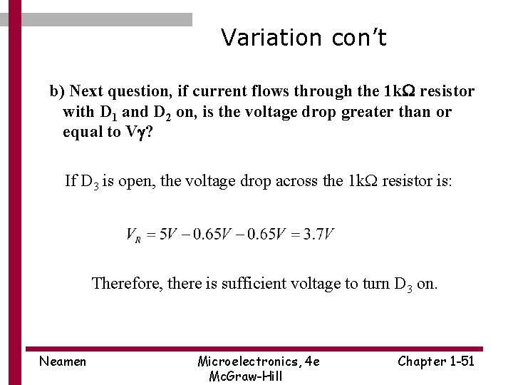
Variation con’t b) Next question, if current flows through the 1 k. W resistor with D 1 and D 2 on, is the voltage drop greater than or equal to Vg? If D 3 is open, the voltage drop across the 1 k. W resistor is: Therefore, there is sufficient voltage to turn D 3 on. Neamen Microelectronics, 4 e Mc. Graw-Hill Chapter 1 -51

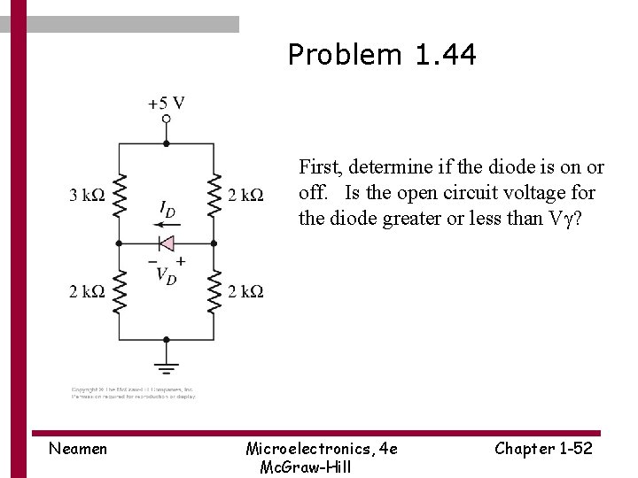
Problem 1. 44 First, determine if the diode is on or off. Is the open circuit voltage for the diode greater or less than Vg? Neamen Microelectronics, 4 e Mc. Graw-Hill Chapter 1 -52

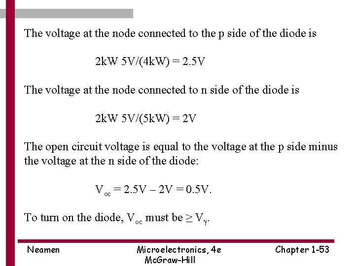
The voltage at the node connected to the p side of the diode is 2 k. W 5 V/(4 k. W) = 2. 5 V The voltage at the node connected to n side of the diode is 2 k. W 5 V/(5 k. W) = 2 V The open circuit voltage is equal to the voltage at the p side minus the voltage at the n side of the diode: Voc = 2. 5 V – 2 V = 0. 5 V. To turn on the diode, Voc must be ≥ Vg. Neamen Microelectronics, 4 e Mc. Graw-Hill Chapter 1 -53

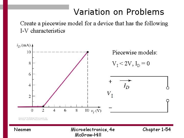
Variation on Problems Create a piecewise model for a device that has the following I-V characteristics Piecewise models: VI < 2 V, ID = 0 Neamen Microelectronics, 4 e Mc. Graw-Hill Chapter 1 -54

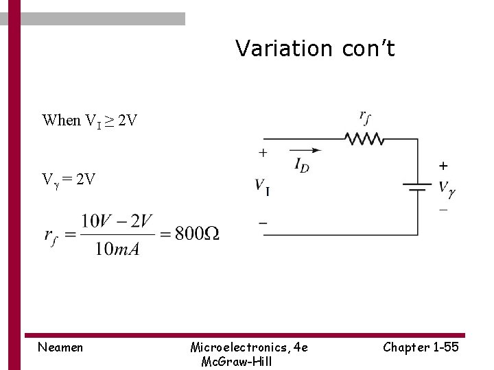
Variation con’t When VI ≥ 2 V Vg = 2 V Neamen Microelectronics, 4 e Mc. Graw-Hill Chapter 1 -55

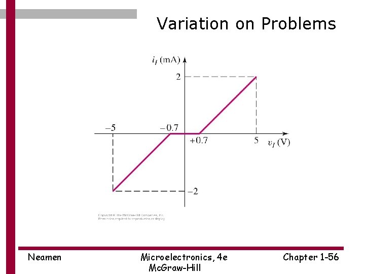
Variation on Problems Neamen Microelectronics, 4 e Mc. Graw-Hill Chapter 1 -56

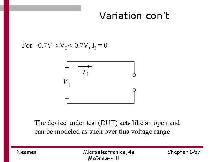
Variation con’t For -0. 7 V < VI < 0. 7 V, II = 0 The device under test (DUT) acts like an open and can be modeled as such over this voltage range. Neamen Microelectronics, 4 e Mc. Graw-Hill Chapter 1 -57

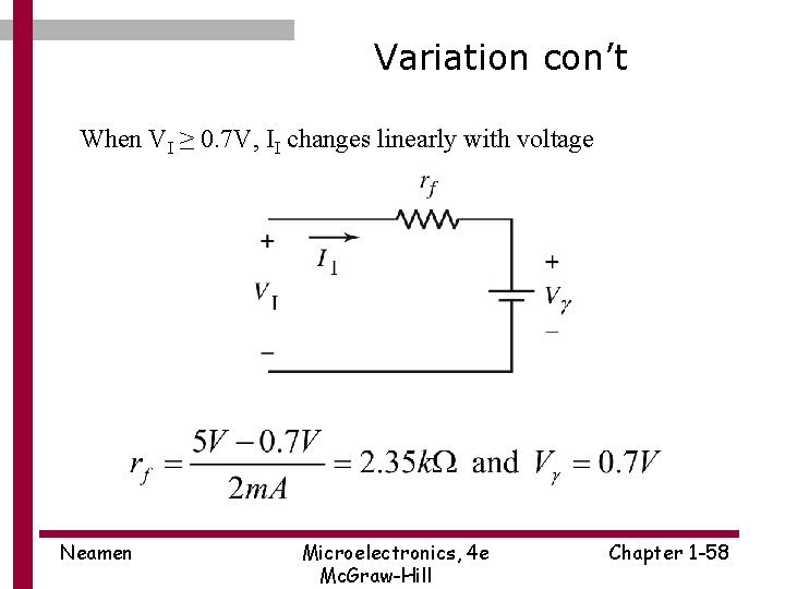
Variation con’t When VI ≥ 0. 7 V, II changes linearly with voltage Neamen Microelectronics, 4 e Mc. Graw-Hill Chapter 1 -58

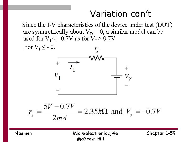
Variation con’t Since the I-V characteristics of the device under test (DUT) are symmetrically about VD = 0, a similar model can be used for VI ≤ - 0. 7 V as for VI ≥ 0. 7 V For VI ≤ - 0. 7 V: Neamen Microelectronics, 4 e Mc. Graw-Hill Chapter 1 -59

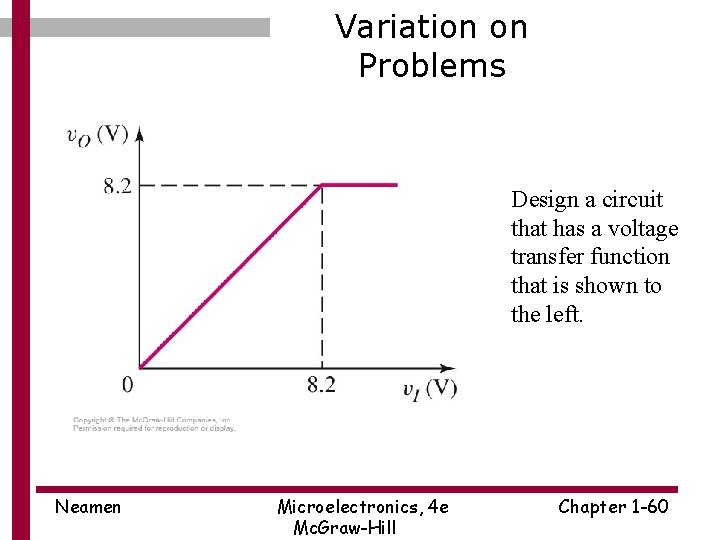
Variation on Problems Design a circuit that has a voltage transfer function that is shown to the left. Neamen Microelectronics, 4 e Mc. Graw-Hill Chapter 1 -60

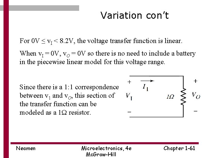
Variation con’t For 0 V ≤ v. I < 8. 2 V, the voltage transfer function is linear. When v. I = 0 V, v. O = 0 V so there is no need to include a battery in the piecewise linear model for this voltage range. Since there is a 1: 1 correspondence between v 1 and v. O, this section of the transfer function can be modeled as a 1 W resistor. Neamen Microelectronics, 4 e Mc. Graw-Hill Chapter 1 -61

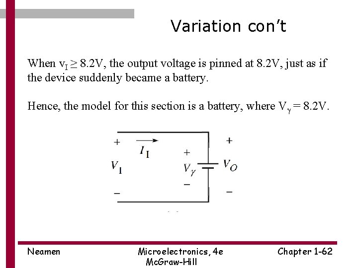
Variation con’t When v. I ≥ 8. 2 V, the output voltage is pinned at 8. 2 V, just as if the device suddenly became a battery. Hence, the model for this section is a battery, where Vg = 8. 2 V. Neamen Microelectronics, 4 e Mc. Graw-Hill Chapter 1 -62

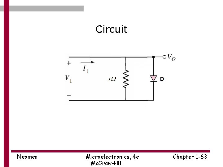
Circuit Neamen Microelectronics, 4 e Mc. Graw-Hill Chapter 1 -63

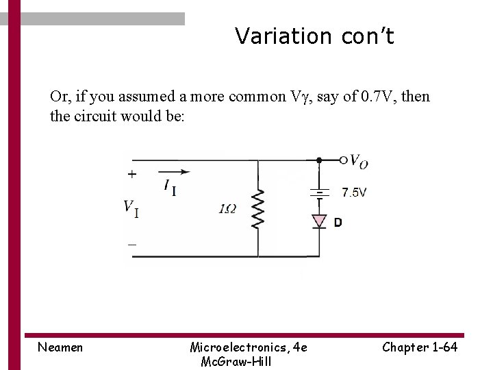
Variation con’t Or, if you assumed a more common Vg, say of 0. 7 V, then the circuit would be: Neamen Microelectronics, 4 e Mc. Graw-Hill Chapter 1 -64