
Lecture 15 Introduction to Integrated Circuit Design What





- Slides: 21
Lecture 15 Introduction to Integrated Circuit Design What if. . . optimizations
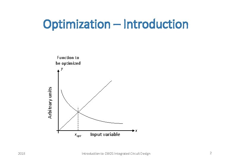
Optimization – Introduction Function to be optimized y Arbitrary units xopt 2018 Input variable x Introduction to CMOS Integrated Circuit Design 2
Inverter pair delay Question: What if we want to minimize the inverter pair delay, how should we choose the width of the p-channel device wrt the width of the nchannel device - considering the difference in electron and hole mobility? Answer: Assume RP=m. RN for the same channel widths. Typically m=2 VDD Rise delay: Fall delay: VIN Normalized pair delay : CN VSS 2018 VSS Minimum pair delay for: Introduction to CMOS Integrated Circuit Design 3
Inverter pair delay Question: What if we want to minimize the inverter pair delay, how should we choose the width of the p-channel device wrt the width of the nchannel device - considering the difference in electron and hole mobility? Answer: Assume RP=m. RN for the same channel widths. Typically m=2 Rise delay: Fall delay: Normalized pair delay : Minimum pair delay for: 2018 Introduction to CMOS Integrated Circuit Design 4
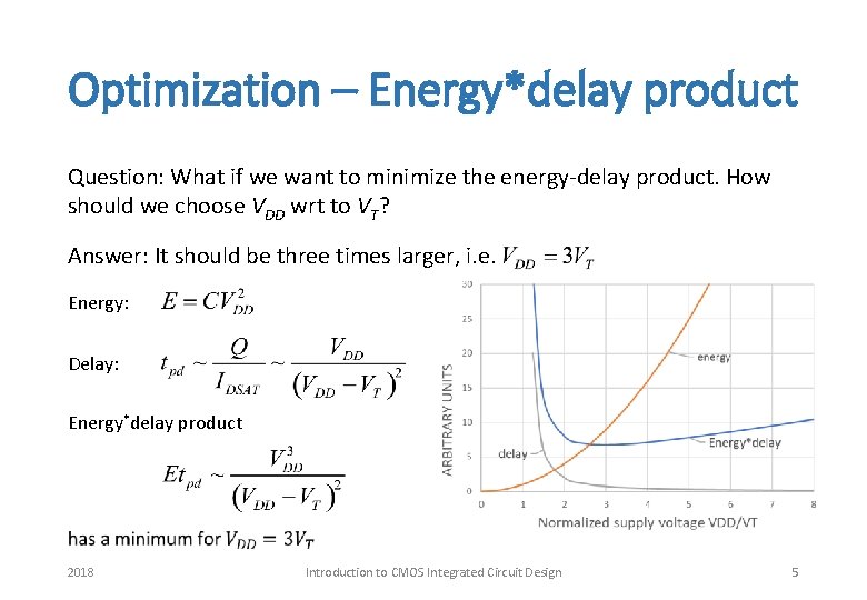
Optimization – Energy*delay product Question: What if we want to minimize the energy-delay product. How should we choose VDD wrt to VT? Answer: It should be three times larger, i. e. Energy: Delay: Energy*delay product 2018 Introduction to CMOS Integrated Circuit Design 5
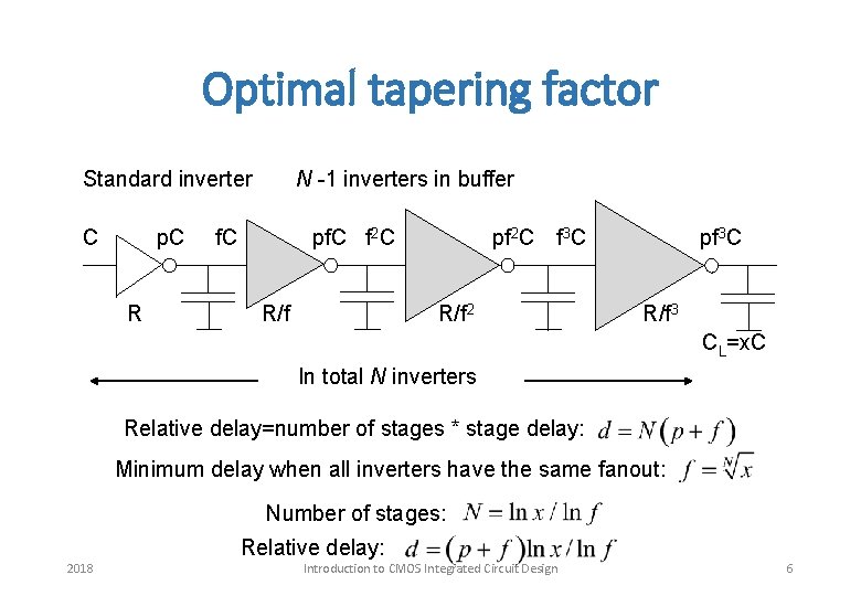
Optimal tapering factor Standard inverter C p. C R N -1 inverters in buffer f. C pf. C f 2 C R/f pf 2 C f 3 C R/f 2 pf 3 C R/f 3 CL=x. C In total N inverters Relative delay=number of stages * stage delay: Minimum delay when all inverters have the same fanout: Number of stages: Relative delay: 2018 Introduction to CMOS Integrated Circuit Design 6
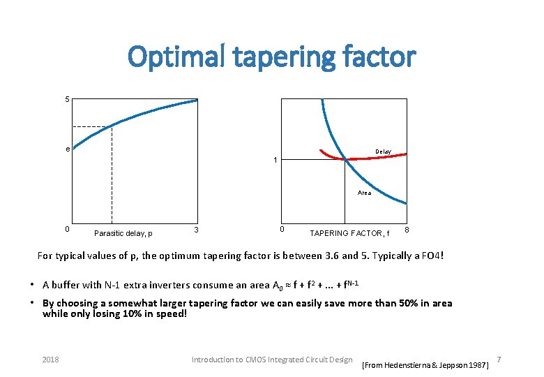
Optimal tapering factor 5 e Delay 1 Area 0 Parasitic delay, p 3 0 TAPERING FACTOR, f 8 For typical values of p, the optimum tapering factor is between 3. 6 and 5. Typically a FO 4! • A buffer with N-1 extra inverters consume an area A 0 ≈ f + f 2 +. . . + f. N-1 • By choosing a somewhat larger tapering factor we can easily save more than 50% in area while only losing 10% in speed! 2018 Introduction to CMOS Integrated Circuit Design [From Hedenstierna & Jeppson 1987] 7
Optimization – Number of inputs Question: What if we were to build a 16 -bit AND gate using n-input NAND/ NOR-gate combinations, what would be the most efficient number of gate inputs to minimize the delay? (Reminder: ) Answer: Is it with 2 - or 4 -input gates? Or with 8 -input gates? 2018 2 -input NAND-NOR gates 4 -input NAND-NOR gates 16 -bit AND gate Introduction to CMOS Integrated Circuit Design 8
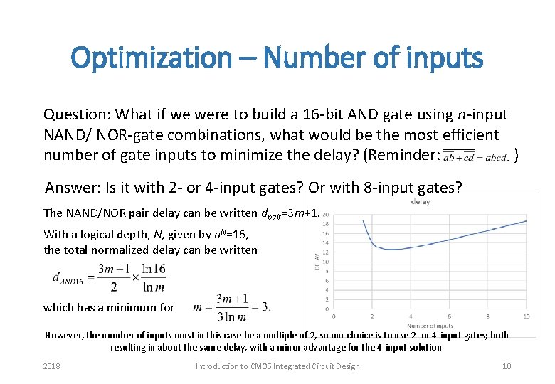
Optimization – Number of inputs Question: What if we were to build a 16 -bit AND gate using n-input NAND/ NOR-gate combinations, what would be the most efficient number of gate inputs to minimize the delay? (Reminder: ) Answer: Is it with 2 - or 4 -input gates? Or with 8 -input gates? The NAND/NOR pair delay can be written dpair=3 m+1. With a logical depth, N, given by n. N=16, the total normalized delay can be written A B & ≥ 1 which has a minimum for C D Y & However, the number of inputs must in this case be a multiple of 2, so our choice is to use 2 - or 4 -input gates; both resulting in about the same delay, with a minor advantage for the 4 -input solution. 2018 Introduction to CMOS Integrated Circuit Design 9
Optimization – Number of inputs Question: What if we were to build a 16 -bit AND gate using n-input NAND/ NOR-gate combinations, what would be the most efficient number of gate inputs to minimize the delay? (Reminder: ) Answer: Is it with 2 - or 4 -input gates? Or with 8 -input gates? The NAND/NOR pair delay can be written dpair=3 m+1. With a logical depth, N, given by n. N=16, the total normalized delay can be written which has a minimum for However, the number of inputs must in this case be a multiple of 2, so our choice is to use 2 - or 4 -input gates; both resulting in about the same delay, with a minor advantage for the 4 -input solution. 2018 Introduction to CMOS Integrated Circuit Design 10
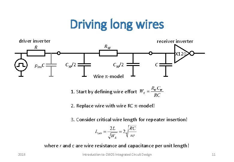
Driving long wires driver inverter R X 120 pinv. C RRw, C W w CW/2 receiver inverter X 120 C Wire p-model 1. Start by defining wire effort 2. Replace wire with wire RC p-model! 3. Consider critical wire length for repeater insertion! where r and c are wire resistance and capacitance per unit length! 2018 Introduction to CMOS Integrated Circuit Design 11
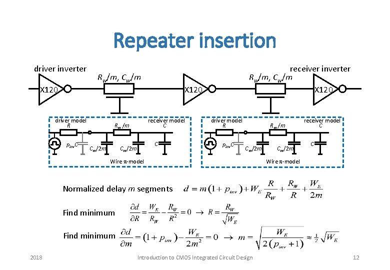
Repeater insertion driver inverter X 120 Rw/m, Cw/m driver model R pinv. C CW/2 m X 120 receiver model C RW /m C CW/2 m receiver inverter Rw/m, Cw/m X 120 driver model R pinv. C RW /m CW/2 m Wire p-model CW/2 m receiver model C C Wire p-model Normalized delay m segments Find minimum 2018 Introduction to CMOS Integrated Circuit Design 12
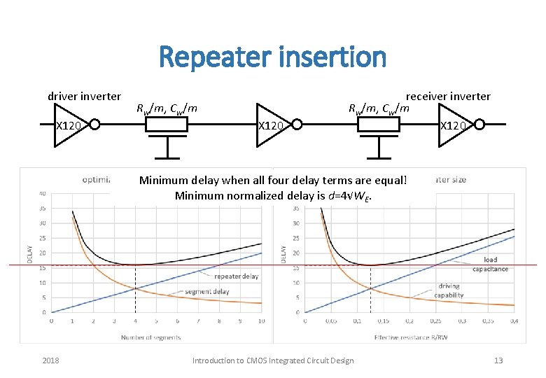
Repeater insertion driver inverter X 120 Rw/m, Cw/m X 120 receiver inverter Rw/m, Cw/m X 120 Minimum delay when all four delay terms are equal! Minimum normalized delay is d=4√WE. 2018 Introduction to CMOS Integrated Circuit Design 13
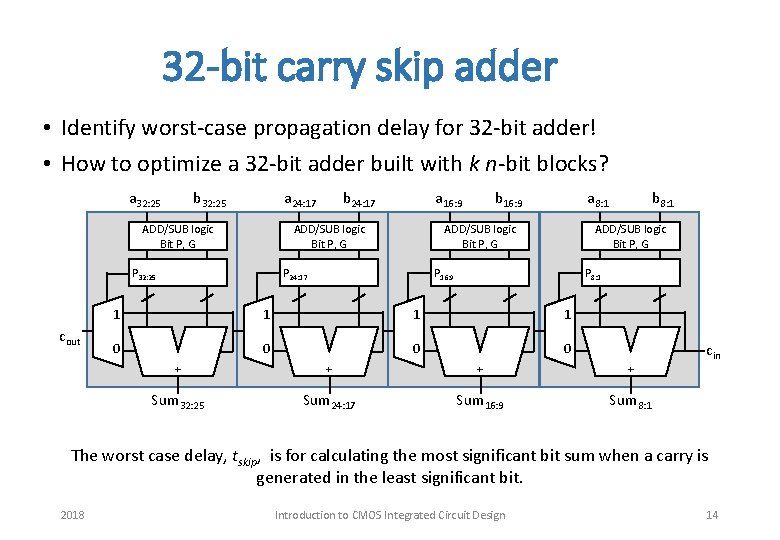
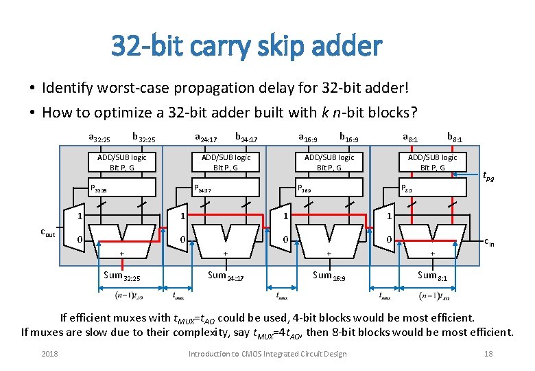
32 -bit carry skip adder • Identify worst-case propagation delay for 32 -bit adder! • How to optimize a 32 -bit adder built with k n-bit blocks? a 32: 25 b 32: 25 a 24: 17 b 24: 17 a 16: 9 b 16: 9 a 8: 1 b 8: 1 ADD/SUB logic Bit P, G P 32: 25 cout P 24: 17 P 16: 9 P 8: 1 1 1 0 0 + + Sum 32: 25 Sum 24: 17 Sum 16: 9 Sum 8: 1 cin The worst case delay, tskip, is for calculating the most significant bit sum when a carry is generated in the least significant bit. 2018 Introduction to CMOS Integrated Circuit Design 14
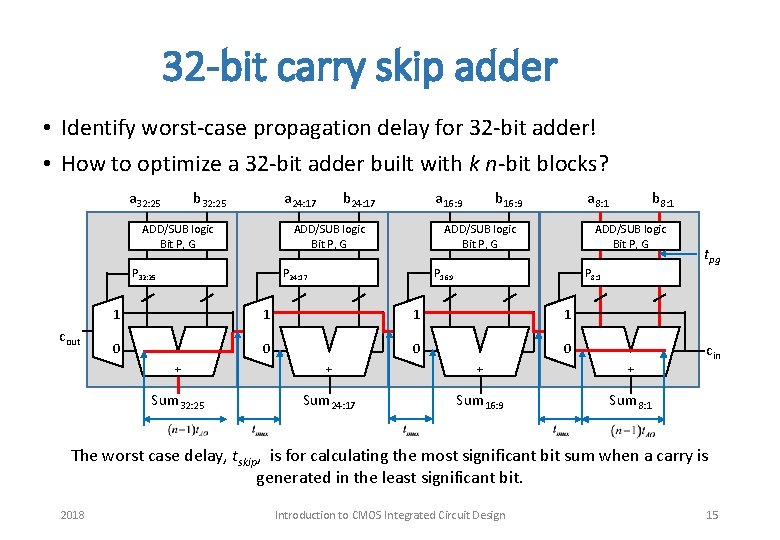
32 -bit carry skip adder • Identify worst-case propagation delay for 32 -bit adder! • How to optimize a 32 -bit adder built with k n-bit blocks? a 32: 25 b 32: 25 a 24: 17 b 24: 17 a 16: 9 b 16: 9 a 8: 1 b 8: 1 ADD/SUB logic Bit P, G P 32: 25 cout P 24: 17 P 16: 9 P 8: 1 1 1 0 0 + + Sum 32: 25 Sum 24: 17 Sum 16: 9 Sum 8: 1 tpg cin The worst case delay, tskip, is for calculating the most significant bit sum when a carry is generated in the least significant bit. 2018 Introduction to CMOS Integrated Circuit Design 15
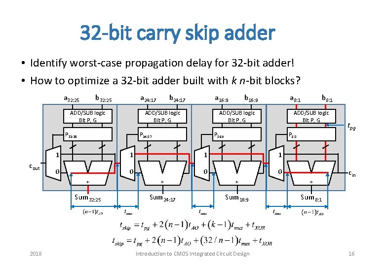
32 -bit carry skip adder • Identify worst-case propagation delay for 32 -bit adder! • How to optimize a 32 -bit adder built with k n-bit blocks? a 32: 25 b 32: 25 a 24: 17 b 24: 17 a 16: 9 b 16: 9 a 8: 1 b 8: 1 ADD/SUB logic Bit P, G P 32: 25 cout 2018 P 24: 17 P 16: 9 P 8: 1 1 1 0 0 + + Sum 32: 25 Sum 24: 17 Sum 16: 9 Sum 8: 1 Introduction to CMOS Integrated Circuit Design tpg cin 16
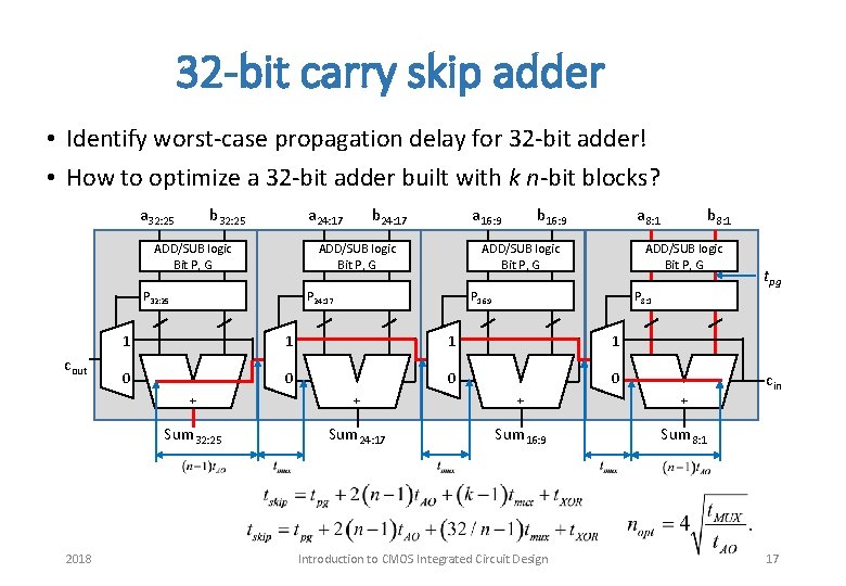
32 -bit carry skip adder • Identify worst-case propagation delay for 32 -bit adder! • How to optimize a 32 -bit adder built with k n-bit blocks? a 32: 25 b 32: 25 a 24: 17 b 24: 17 a 16: 9 b 16: 9 a 8: 1 b 8: 1 ADD/SUB logic Bit P, G P 32: 25 cout 2018 P 24: 17 P 16: 9 P 8: 1 1 1 0 0 + + Sum 32: 25 Sum 24: 17 Sum 16: 9 Sum 8: 1 Introduction to CMOS Integrated Circuit Design tpg cin 17
32 -bit carry skip adder • Identify worst-case propagation delay for 32 -bit adder! • How to optimize a 32 -bit adder built with k n-bit blocks? a 32: 25 b 32: 25 a 24: 17 b 24: 17 a 16: 9 b 16: 9 a 8: 1 b 8: 1 ADD/SUB logic Bit P, G P 32: 25 cout P 24: 17 P 16: 9 P 8: 1 1 1 0 0 + + Sum 32: 25 Sum 24: 17 Sum 16: 9 Sum 8: 1 tpg cin If efficient muxes with t. MUX=t. AO could be used, 4 -bit blocks would be most efficient. If muxes are slow due to their complexity, say t. MUX=4 t. AO, then 8 -bit blocks would be most efficient. 2018 Introduction to CMOS Integrated Circuit Design 18
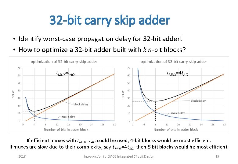
32 -bit carry skip adder • Identify worst-case propagation delay for 32 -bit adder! • How to optimize a 32 -bit adder built with k n-bit blocks? a 32: 25 b 32: 25 ADD/SUB logic t. MUX=t. AO Bit P, G P 32: 25 cout a 24: 17 b 24: 17 a 16: 9 b 16: 9 ADD/SUB logic Bit P, G P 24: 17 a 8: 1 b 8: 1 ADD/SUB logic t. MUX=4 t. AOBit P, G P 16: 9 P 8: 1 1 1 0 0 + + Sum 32: 25 Sum 24: 17 Sum 16: 9 Sum 8: 1 tpg cin If efficient muxes with t. MUX=t. AO could be used, 4 -bit blocks would be most efficient. If muxes are slow due to their complexity, say t. MUX=4 t. AO, then 8 -bit blocks would be most efficient. 2018 Introduction to CMOS Integrated Circuit Design 19
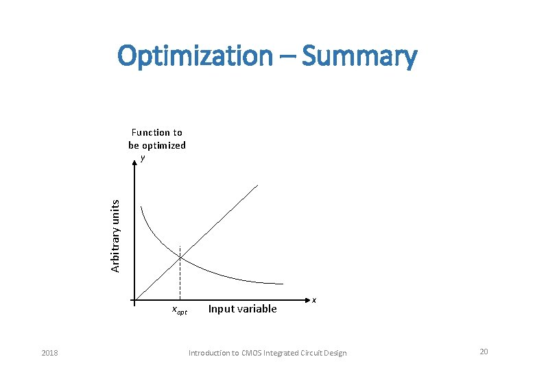
Optimization – Summary Function to be optimized y Arbitrary units xopt 2018 Input variable x Introduction to CMOS Integrated Circuit Design 20
End of ”what if” lecture! Q & A? 2018 Introduction to CMOS Integrated Circuit Design 21