ECE 1352 F 2003 Analog Circuit Design Presentation


![Two-Stage Gate Driver ® To reduce IRR and VCE, overvoltage , [6] suggested the Two-Stage Gate Driver ® To reduce IRR and VCE, overvoltage , [6] suggested the](https://slidetodoc.com/presentation_image_h/c163925f7828b937a5c0c52a79a650e7/image-11.jpg)
![Active Gate Control ® [5] suggested an active, independent dv/dt and di/dt control techniques Active Gate Control ® [5] suggested an active, independent dv/dt and di/dt control techniques](https://slidetodoc.com/presentation_image_h/c163925f7828b937a5c0c52a79a650e7/image-14.jpg)
![Voltage Balancing ® [7] suggested a multi-level clamp and turn-off timing adjustment driver to Voltage Balancing ® [7] suggested a multi-level clamp and turn-off timing adjustment driver to](https://slidetodoc.com/presentation_image_h/c163925f7828b937a5c0c52a79a650e7/image-19.jpg)
![Voltage Balancing ® [8] suggested another way of balancing the voltage by connecting a Voltage Balancing ® [8] suggested another way of balancing the voltage by connecting a](https://slidetodoc.com/presentation_image_h/c163925f7828b937a5c0c52a79a650e7/image-20.jpg)
![References ® ECE 1352 Term Papers: [1] O. Trescases, “ECE 1352 Term Paper: Integrated References ® ECE 1352 Term Papers: [1] O. Trescases, “ECE 1352 Term Paper: Integrated](https://slidetodoc.com/presentation_image_h/c163925f7828b937a5c0c52a79a650e7/image-23.jpg)
![References ® IGBT Gate Drive: [5] S. Park and T. M. Jahns, “Flexible dv/dt References ® IGBT Gate Drive: [5] S. Park and T. M. Jahns, “Flexible dv/dt](https://slidetodoc.com/presentation_image_h/c163925f7828b937a5c0c52a79a650e7/image-24.jpg)
- Slides: 24

ECE 1352 F (2003) Analog Circuit Design Presentation Integrated “Smart Power” IGBT Drivers Kay (Tsz Shuen) Chan 993509681 November 28, 2003

Objectives ® Introduce briefly some of the design considerations of IGBT drivers in power electronics ® Present recent design techniques and circuits for IGBT driver ® Address design future challenges in IGBT driver

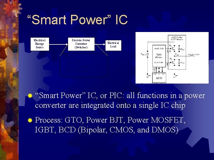
“Smart Power” IC Electrical Energy Source Discrete Power Converter (Switches) Electrical Load Functions: - control logic - protection - diagnostic feedback - power output stage - etc … ® “Smart Power” IC, or PIC: all functions in a power converter are integrated onto a single IC chip ® Process: GTO, Power BJT, Power MOSFET, IGBT, BCD (Bipolar, CMOS, and DMOS)

“Smart Power” IC ® Design goals: Manage voltage and current of the device within the rating levels ® Minimize power dissipation ® ® Use as few parts as possible ® Applications: Electric power transmission ® UPS power supplies ® Switchmode power supplies ® Automotive ® Motor Control ® Household appliances ®

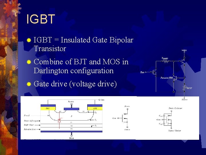
IGBT ® IGBT = Insulated Gate Bipolar Transistor ® Combine of BJT and MOS in Darlington configuration ® Gate drive (voltage drive)

IGBT: Switches in PIC ® Compared to BJT and Power-MOS, IGBT has ® Higher on-state voltage and current density ® Higher input impedance ® Rapid switching times ® Lower conduction losses ® Less silicon area because the gate driver circuit is simpler ® Becomes a popular switching device in medium and high power applications (>100 W) ® To increase voltage rating (>1000 V), need to use series-connected IGBTs

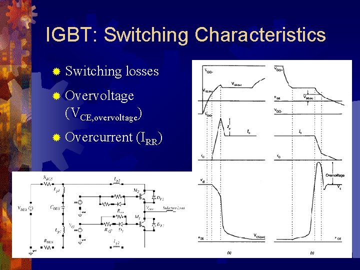
IGBT: Switching Characteristics ® Switching losses ® Overvoltage (VCE, overvoltage) ® Overcurrent (IRR)

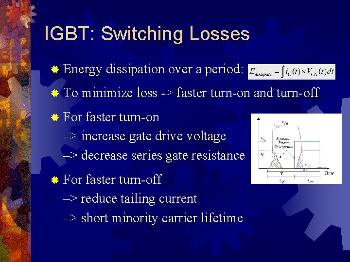
IGBT: Switching Losses ® Energy ® To dissipation over a period: minimize loss -> faster turn-on and turn-off ® For faster turn-on –> increase gate drive voltage –> decrease series gate resistance ® For faster turn-off –> reduce tailing current –> short minority carrier lifetime

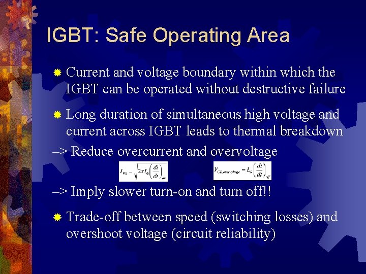
IGBT: Safe Operating Area ® Current and voltage boundary within which the IGBT can be operated without destructive failure ® Long duration of simultaneous high voltage and current across IGBT leads to thermal breakdown –> Reduce overcurrent and overvoltage –> Imply slower turn-on and turn off!! ® Trade-off between speed (switching losses) and overshoot voltage (circuit reliability)

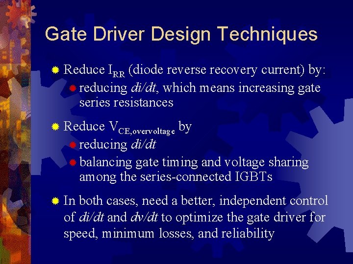
Gate Driver Design Techniques ® Reduce IRR (diode reverse recovery current) by: ® reducing di/dt, which means increasing gate series resistances ® Reduce VCE, overvoltage by ® reducing di/dt ® balancing gate timing and voltage sharing among the series-connected IGBTs ® In both cases, need a better, independent control of di/dt and dv/dt to optimize the gate driver for speed, minimum losses, and reliability
![TwoStage Gate Driver To reduce IRR and VCE overvoltage 6 suggested the Two-Stage Gate Driver ® To reduce IRR and VCE, overvoltage , [6] suggested the](https://slidetodoc.com/presentation_image_h/c163925f7828b937a5c0c52a79a650e7/image-11.jpg)
Two-Stage Gate Driver ® To reduce IRR and VCE, overvoltage , [6] suggested the following two-stage driver circuit ® Turn-on: RGon 2 << RGon 1 ® Stage-2 is off initially ® Cgate charged through RGon 1 (larger) to keep IRR small ® After diode has recovered, stage-2 turn on (triggered by VREF in comparator) ® Driver resistance is now RGon 1||RGon 2 (smaller) ®

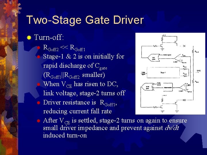
Two-Stage Gate Driver ® Turn-off: ® RGoff 2 << RGoff 1 ® Stage-1 & 2 is on initially for rapid discharge of Cgate (RGoff 1||RGoff 2 smaller) ® When VCE has risen to DC, link voltage, stage-2 turns off ® Driver resistance is RGoff 1, reducing current fall rate ® After VCE is settled, stage-2 turns on again to ensure small driver impedance and prevent against dv/dt induced turn-on

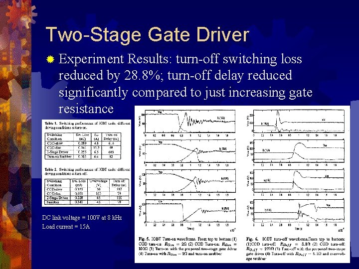
Two-Stage Gate Driver ® Experiment Results: turn-off switching loss reduced by 28. 8%; turn-off delay reduced significantly compared to just increasing gate resistance DC link voltage = 100 V at 8 k. Hz Load current = 15 A
![Active Gate Control 5 suggested an active independent dvdt and didt control techniques Active Gate Control ® [5] suggested an active, independent dv/dt and di/dt control techniques](https://slidetodoc.com/presentation_image_h/c163925f7828b937a5c0c52a79a650e7/image-14.jpg)
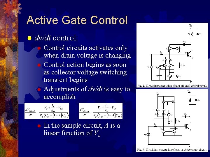
Active Gate Control ® [5] suggested an active, independent dv/dt and di/dt control techniques by means of feedback (Miller effect) ® dv/dt control: ® Add Miller capacitance connecting gate and collector ® Add, at gate node, a dependent current source whose current is proportional to capacitor current ® Net current at gate node is Im(1 -A). By adjusting A, can change the total capacitance across gate and collector, and thus changing dv/dt

Active Gate Control ® dv/dt control: ® Control circuits activates only when drain voltage is changing ® Control action begins as soon as collector voltage switching transient begins ® Adjustments of dv/dt is easy to accomplish ® In the sample circuit, A is a linear function of Vc

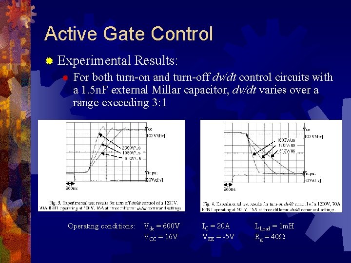
Active Gate Control ® Experimental Results: ® For both turn-on and turn-off dv/dt control circuits with a 1. 5 n. F external Millar capacitor, dv/dt varies over a range exceeding 3: 1 Operating conditions: Vdc = 600 V VCC = 16 V IC = 20 A VEE = -5 V LLoad = 1 m. H Rg = 40

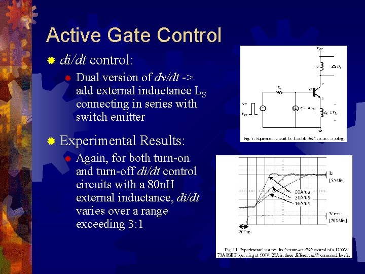
Active Gate Control ® di/dt control: ® Dual version of dv/dt -> add external inductance LS connecting in series with switch emitter ® Experimental Results: ® Again, for both turn-on and turn-off di/dt control circuits with a 80 n. H external inductance, di/dt varies over a range exceeding 3: 1

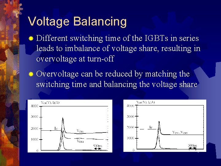
Voltage Balancing ® Different switching time of the IGBTs in series leads to imbalance of voltage share, resulting in overvoltage at turn-off ® Overvoltage can be reduced by matching the switching time and balancing the voltage share
![Voltage Balancing 7 suggested a multilevel clamp and turnoff timing adjustment driver to Voltage Balancing ® [7] suggested a multi-level clamp and turn-off timing adjustment driver to](https://slidetodoc.com/presentation_image_h/c163925f7828b937a5c0c52a79a650e7/image-19.jpg)
Voltage Balancing ® [7] suggested a multi-level clamp and turn-off timing adjustment driver to balance the voltage ® Overvoltage reduces from 3700 V to 3300 V ® Turn-off timings within 100 ns
![Voltage Balancing 8 suggested another way of balancing the voltage by connecting a Voltage Balancing ® [8] suggested another way of balancing the voltage by connecting a](https://slidetodoc.com/presentation_image_h/c163925f7828b937a5c0c52a79a650e7/image-20.jpg)
Voltage Balancing ® [8] suggested another way of balancing the voltage by connecting a simple iron core and coils at the gate

Future Challenges ® How to best utilize the control techniques in future generations of gate drive circuits ® In particular, how to optimize the gate drive circuits for a even better timing and switching losses while keeping the circuits compact ® As the voltage and current ratings increase, new techniques are in need to ensure circuit protection and reliability

Future Challenges ® Recent IEEE papers have presented analysis of IGBT operation under short-circuit, over temperature, hard switching fault, and fault under load conditions (next step -> gate drive circuits realization) ® IGBT process has been evolving, leading to new concerns in gate driver design
![References ECE 1352 Term Papers 1 O Trescases ECE 1352 Term Paper Integrated References ® ECE 1352 Term Papers: [1] O. Trescases, “ECE 1352 Term Paper: Integrated](https://slidetodoc.com/presentation_image_h/c163925f7828b937a5c0c52a79a650e7/image-23.jpg)
References ® ECE 1352 Term Papers: [1] O. Trescases, “ECE 1352 Term Paper: Integrated “Smart Power” IGBT Drivers”, 2003. ® IGBT Process: [2] M. H. Rashid, Power Electronics Handbook, San Diego: Academic Press, 2001. [3] N. Kularatna, Power Electronics Design Handbook: Low-Power Components and Applications, Boston: Newnes, 1998. ® IGBT Gate Drive: [4] R. S. Chokhawala, J. Catt, and B. R. Pelly, “Gate Drive Considerations for IGBT Modules, ” Industry Applications, IEEE Transactions on, vol. 31, no. 3, pp. 603 -611, May-June 1995.
![References IGBT Gate Drive 5 S Park and T M Jahns Flexible dvdt References ® IGBT Gate Drive: [5] S. Park and T. M. Jahns, “Flexible dv/dt](https://slidetodoc.com/presentation_image_h/c163925f7828b937a5c0c52a79a650e7/image-24.jpg)
References ® IGBT Gate Drive: [5] S. Park and T. M. Jahns, “Flexible dv/dt and di/dt Control Method for Insulated Gate Power Switches, ” Industry Applications Conference, 2001. 36 th IAS Annual Meeting. Conference Record of the 2001 IEEE, vol. 2, pp. 1038 -1045, Sept-Oct 2001. [6] R. Sachdeva and E. P. Nowicki, “A Novel Gate Driver Circuit for Snubberless, Low-Noise Operation of High Power IGBT, ” Electrical and Computer Engineering, 2002. IEEE CCECE 2002. Canadian Conference, vol. 1, pp. 212 -217, May 2002. [7] H. Nakatake and A. Iwata, “Series Connection of IGBTs used Multi-Level Clamp Circuit and Turn Off Timing Adjustment Circuit, ” Power Electronics Specialist, 2003. PESC '03. IEEE 34 th Annual Conference, vol. 4, pp. 19101915, June 2003. [8] K. Sasagawa, Y. Abe, and K. Matsuse, “Voltage Balancing Method for IGBTs Connected in Series, ” Industry Applications Conference, 2002. 37 th IAS Annual Meeting. Conference Record, vol. 4, pp. 2597 -2602, Oct 2002.