CERN Technical Training 2005 ELEC2005 Electronics in High
- Slides: 38
CERN Technical Training 2005 ELEC-2005 Electronics in High Energy Physics Spring term: Integrated circuits and VLSI technology for physics Basic Analog Design Giovanni Anelli 15 March 2005 Part II ELEC 2005 Giovanni Anelli - CERN
Outline – Part II • • ELEC 2005 Noise in analog ICs Matching in analog ICs Operational Amplifier design examples Analog design methodology Giovanni Anelli - CERN 2
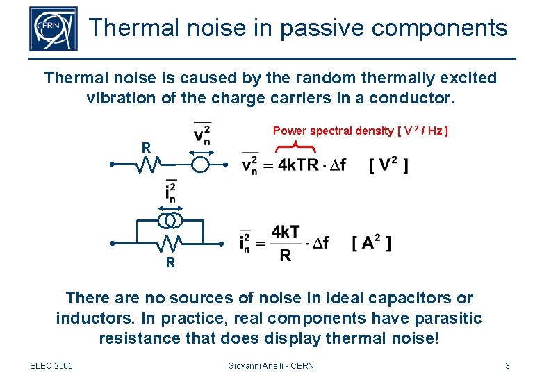
Thermal noise in passive components Thermal noise is caused by the random thermally excited vibration of the charge carriers in a conductor. Power spectral density [ V 2 / Hz ] R R There are no sources of noise in ideal capacitors or inductors. In practice, real components have parasitic resistance that does display thermal noise! ELEC 2005 Giovanni Anelli - CERN 3
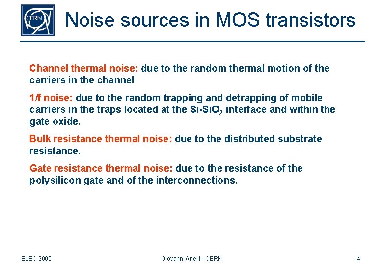
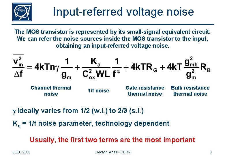
Noise sources in MOS transistors Channel thermal noise: due to the random thermal motion of the carriers in the channel 1/f noise: due to the random trapping and detrapping of mobile carriers in the traps located at the Si-Si. O 2 interface and within the gate oxide. Bulk resistance thermal noise: due to the distributed substrate resistance. Gate resistance thermal noise: due to the resistance of the polysilicon gate and of the interconnections. ELEC 2005 Giovanni Anelli - CERN 4
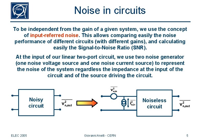
Noise in circuits To be independent from the gain of a given system, we use the concept of input-referred noise. This allows comparing easily the noise performance of different circuits (with different gains), and calculating easily the Signal-to-Noise Ratio (SNR). At the input of our linear two-port circuit, we use two noise generator (one noise voltage source and one noise current source) to represent the noise of the system regardless the impedance at the input of the circuit and of the source driving the circuit. Noisy circuit ELEC 2005 Noiseless circuit Giovanni Anelli - CERN 5
Input-referred voltage noise The MOS transistor is represented by its small-signal equivalent circuit. We can refer the noise sources inside the MOS transistor to the input, obtaining an input-referred voltage noise. Channel thermal noise 1/f noise Gate resistance thermal noise Bulk resistance thermal noise g ideally varies from 1/2 (w. i. ) to 2/3 (s. i. ) Ka = 1/f noise parameter, technology dependent Usually, the first two terms are the most important ELEC 2005 Giovanni Anelli - CERN 6
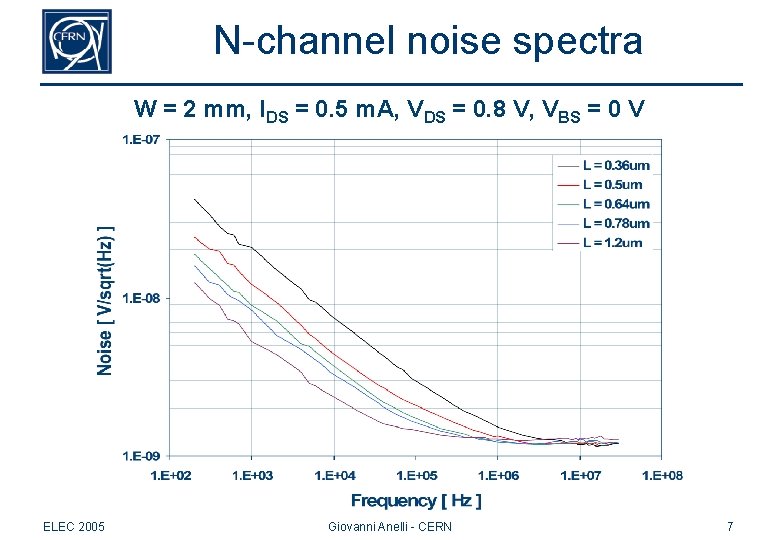
N-channel noise spectra W = 2 mm, IDS = 0. 5 m. A, VDS = 0. 8 V, VBS = 0 V ELEC 2005 Giovanni Anelli - CERN 7
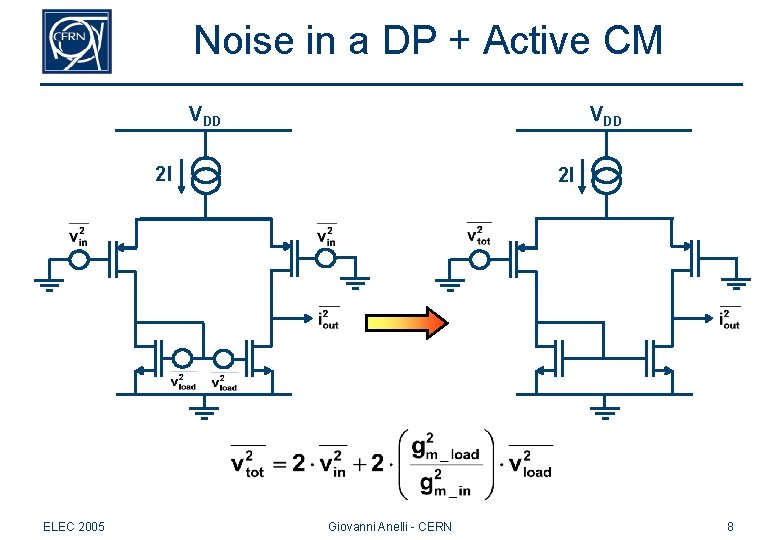
Noise in a DP + Active CM VDD 2 I ELEC 2005 2 I Giovanni Anelli - CERN 8
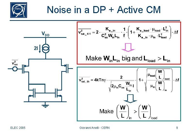
Noise in a DP + Active CM VDD 2 I ELEC 2005 Giovanni Anelli - CERN 9
Outline – Part II • • ELEC 2005 Noise in analog ICs Matching in analog ICs Operational Amplifier design examples Analog design methodology Giovanni Anelli - CERN 10
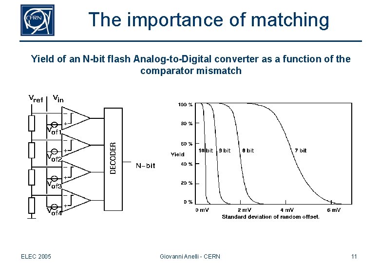
The importance of matching Yield of an N-bit flash Analog-to-Digital converter as a function of the comparator mismatch ELEC 2005 Giovanni Anelli - CERN 11
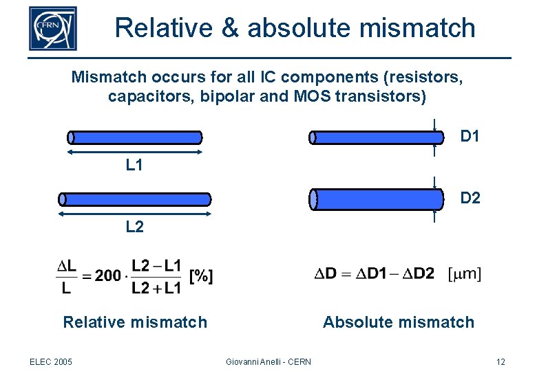
Relative & absolute mismatch Mismatch occurs for all IC components (resistors, capacitors, bipolar and MOS transistors) D 1 L 1 D 2 L 2 Absolute mismatch Relative mismatch ELEC 2005 Giovanni Anelli - CERN 12
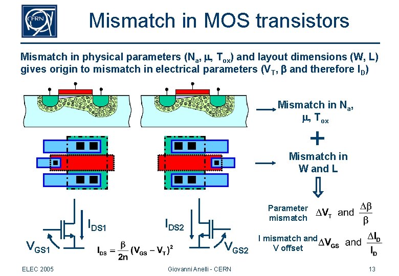
Mismatch in MOS transistors Mismatch in physical parameters (Na, , Tox) and layout dimensions (W, L) gives origin to mismatch in electrical parameters (VT, and therefore ID) Mismatch in Na, , Tox + Mismatch in W and L IDS 1 VGS 1 ELEC 2005 Parameter mismatch IDS 2 VGS 2 Giovanni Anelli - CERN I mismatch and V offset 13
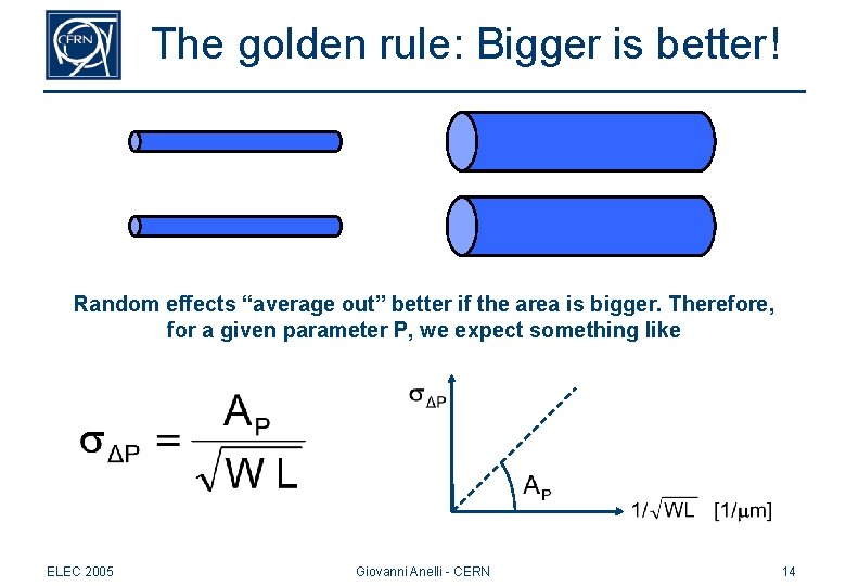
The golden rule: Bigger is better! Random effects “average out” better if the area is bigger. Therefore, for a given parameter P, we expect something like ELEC 2005 Giovanni Anelli - CERN 14
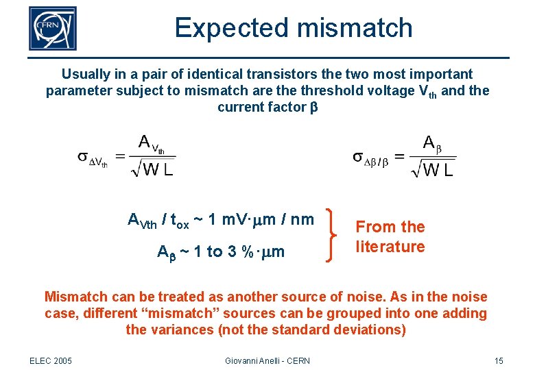
Expected mismatch Usually in a pair of identical transistors the two most important parameter subject to mismatch are threshold voltage Vth and the current factor AVth / tox ~ 1 m. V· m / nm A ~ 1 to 3 %· m From the literature Mismatch can be treated as another source of noise. As in the noise case, different “mismatch” sources can be grouped into one adding the variances (not the standard deviations) ELEC 2005 Giovanni Anelli - CERN 15
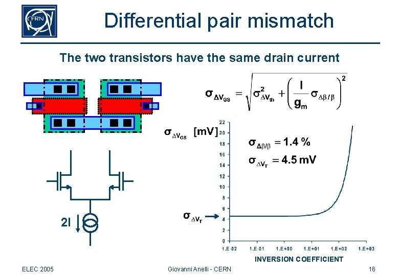
Differential pair mismatch The two transistors have the same drain current 2 I INVERSIONI. C. COEFFICIENT ELEC 2005 Giovanni Anelli - CERN 16
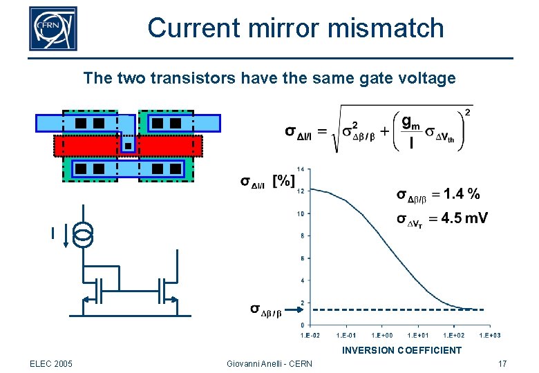
Current mirror mismatch The two transistors have the same gate voltage I I. C. INVERSION COEFFICIENT ELEC 2005 Giovanni Anelli - CERN 17
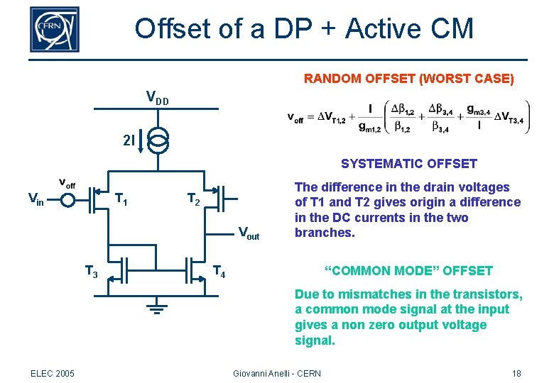
Offset of a DP + Active CM RANDOM OFFSET (WORST CASE) VDD 2 I SYSTEMATIC OFFSET Vin T 1 T 2 Vout T 3 The difference in the drain voltages of T 1 and T 2 gives origin a difference in the DC currents in the two branches. T 4 “COMMON MODE” OFFSET Due to mismatches in the transistors, a common mode signal at the input gives a non zero output voltage signal. ELEC 2005 Giovanni Anelli - CERN 18
Outline – Part II • Noise in analog ICs • Matching in analog ICs • Operational Amplifier design examples Ø Ø Ø Op Amp application examples Single-Stage Op Amps Two-Stage Op Amps Fully Differential Op Amps Feedback and frequency compensation • Analog design methodology ELEC 2005 Giovanni Anelli - CERN 19
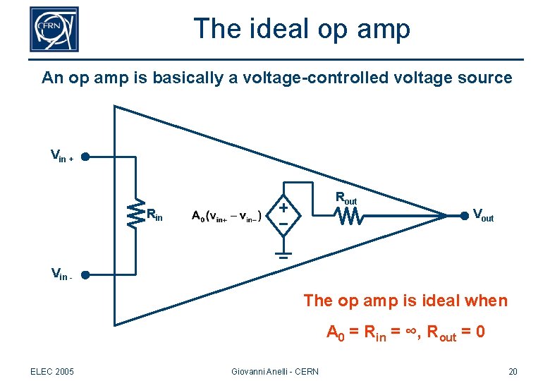
The ideal op amp An op amp is basically a voltage-controlled voltage source Vin + Rout Rin Vout Vin - The op amp is ideal when A 0 = Rin = ∞, Rout = 0 ELEC 2005 Giovanni Anelli - CERN 20
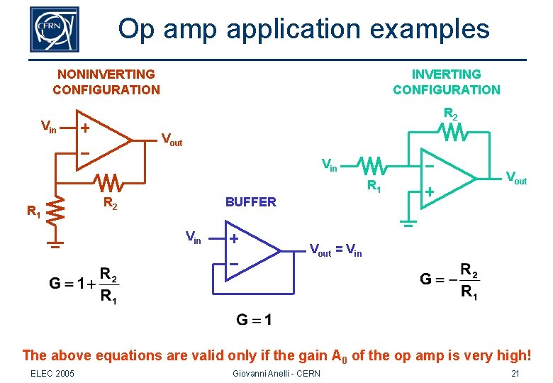
Op amp application examples NONINVERTING CONFIGURATION R 2 Vin Vout Vin R 1 R 2 Vout BUFFER Vin Vout = Vin The above equations are valid only if the gain A 0 of the op amp is very high! ELEC 2005 Giovanni Anelli - CERN 21
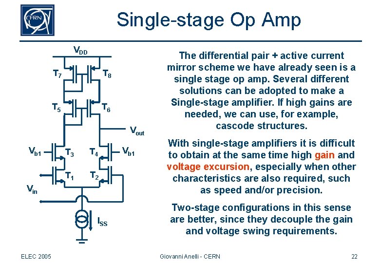
Single-stage Op Amp VDD T 7 T 8 T 5 T 6 Vout Vb 1 T 3 T 4 T 1 T 2 Vin ISS ELEC 2005 Vb 1 The differential pair + active current mirror scheme we have already seen is a single stage op amp. Several different solutions can be adopted to make a Single-stage amplifier. If high gains are needed, we can use, for example, cascode structures. With single-stage amplifiers it is difficult to obtain at the same time high gain and voltage excursion, especially when other characteristics are also required, such as speed and/or precision. Two-stage configurations in this sense are better, since they decouple the gain and voltage swing requirements. Giovanni Anelli - CERN 22
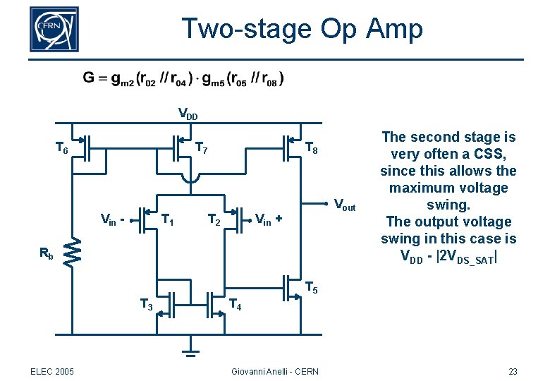
Two-stage Op Amp VDD T 6 T 7 Vin - T 1 T 8 T 2 Vout Vin + Rb The second stage is very often a CSS, since this allows the maximum voltage swing. The output voltage swing in this case is VDD - |2 VDS_SAT| T 5 T 3 ELEC 2005 T 4 Giovanni Anelli - CERN 23
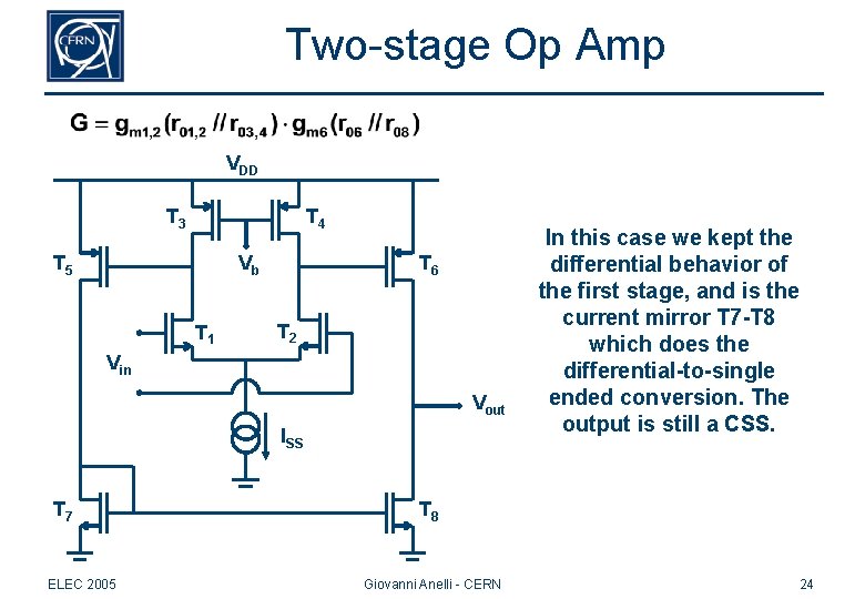
Two-stage Op Amp VDD T 3 T 4 T 5 Vb T 1 T 6 T 2 Vin Vout ISS T 7 ELEC 2005 In this case we kept the differential behavior of the first stage, and is the current mirror T 7 -T 8 which does the differential-to-single ended conversion. The output is still a CSS. T 8 Giovanni Anelli - CERN 24
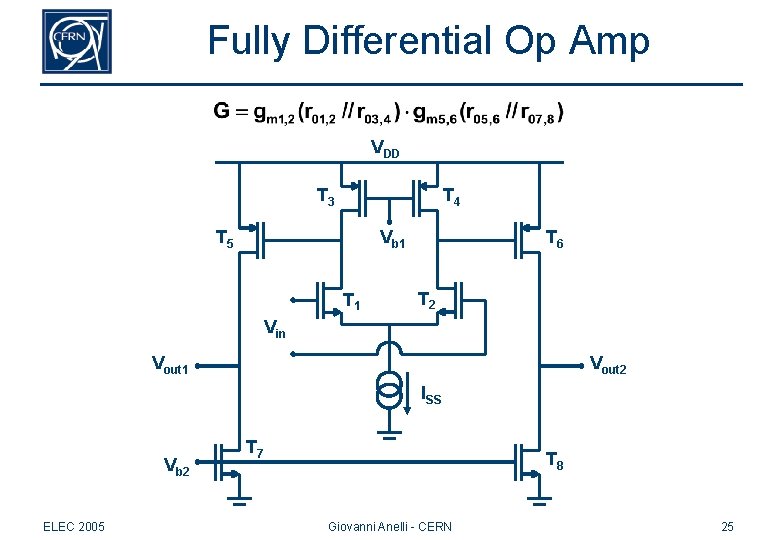
Fully Differential Op Amp VDD T 3 T 4 T 5 Vb 1 T 6 T 2 Vin Vout 1 Vout 2 ISS Vb 2 ELEC 2005 T 7 T 8 Giovanni Anelli - CERN 25
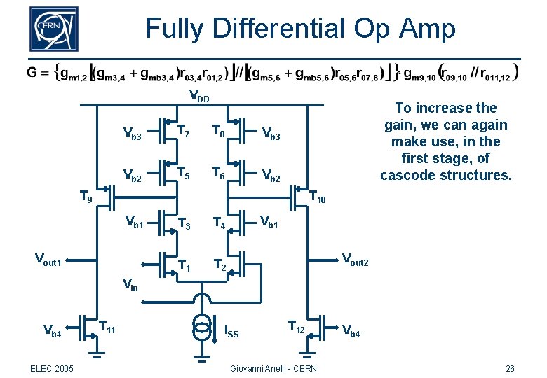
Fully Differential Op Amp VDD Vb 3 T 7 T 8 Vb 3 Vb 2 T 5 T 6 Vb 2 To increase the gain, we can again make use, in the first stage, of cascode structures. T 9 T 10 Vb 1 Vout 1 T 3 T 4 T 1 T 2 Vb 1 Vout 2 Vin Vb 4 ELEC 2005 T 11 ISS T 12 Giovanni Anelli - CERN Vb 4 26
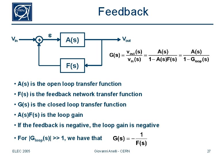
Feedback Vin + e Vout A(s) F(s) • A(s) is the open loop transfer function • F(s) is the feedback network transfer function • G(s) is the closed loop transfer function • A(s)F(s) is the loop gain • If the feedback is negative, the loop gain is negative • For |Gloop(s)| >> 1, we have that ELEC 2005 Giovanni Anelli - CERN 27
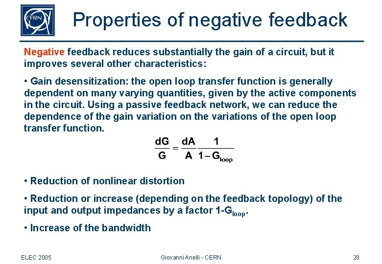
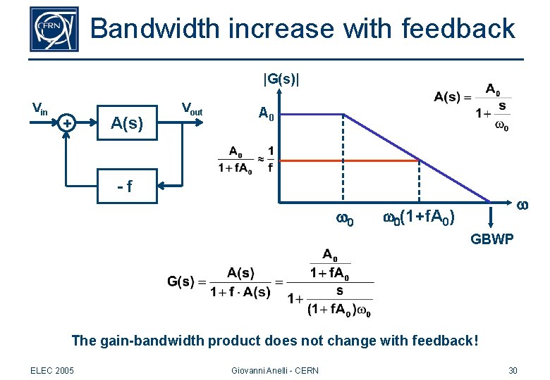
Properties of negative feedback Negative feedback reduces substantially the gain of a circuit, but it improves several other characteristics: • Gain desensitization: the open loop transfer function is generally dependent on many varying quantities, given by the active components in the circuit. Using a passive feedback network, we can reduce the dependence of the gain variation on the variations of the open loop transfer function. • Reduction of nonlinear distortion • Reduction or increase (depending on the feedback topology) of the input and output impedances by a factor 1 -Gloop. • Increase of the bandwidth ELEC 2005 Giovanni Anelli - CERN 28
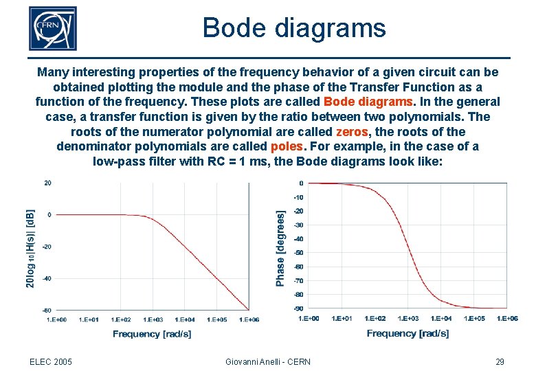
Bode diagrams Many interesting properties of the frequency behavior of a given circuit can be obtained plotting the module and the phase of the Transfer Function as a function of the frequency. These plots are called Bode diagrams. In the general case, a transfer function is given by the ratio between two polynomials. The roots of the numerator polynomial are called zeros, the roots of the denominator polynomials are called poles. For example, in the case of a low-pass filter with RC = 1 ms, the Bode diagrams look like: ELEC 2005 Giovanni Anelli - CERN 29
Bandwidth increase with feedback |G(s)| Vin + A(s) Vout A 0 -f w 0 w w 0(1+f. A 0) GBWP The gain-bandwidth product does not change with feedback! ELEC 2005 Giovanni Anelli - CERN 30
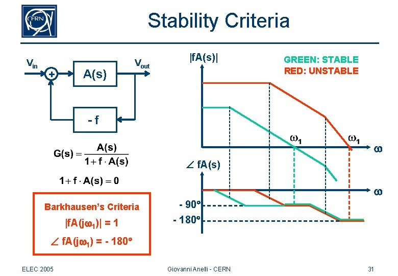
Stability Criteria Vin + A(s) Vout |f. A(s)| GREEN: STABLE RED: UNSTABLE -f w f. A(s) w Barkhausen’s Criteria |f. A(jw 1)| = 1 - 90 - 180 f. A(jw 1) = - 180 ELEC 2005 Giovanni Anelli - CERN 31
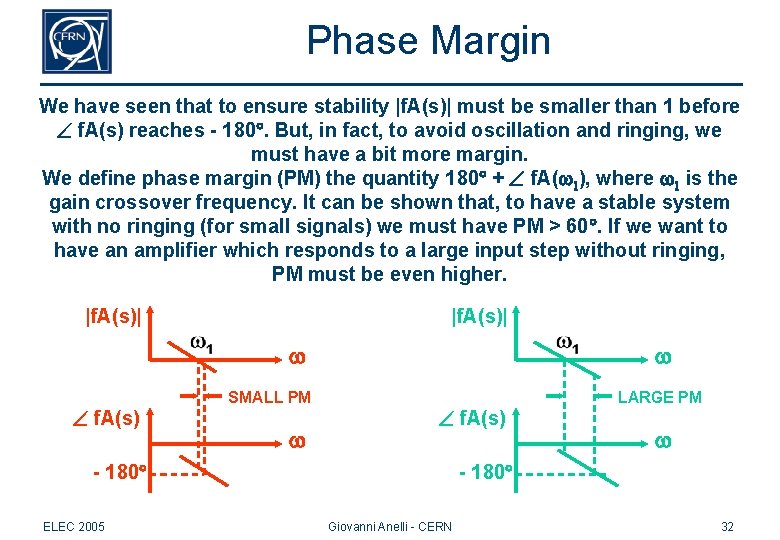
Phase Margin We have seen that to ensure stability |f. A(s)| must be smaller than 1 before f. A(s) reaches - 180. But, in fact, to avoid oscillation and ringing, we must have a bit more margin. We define phase margin (PM) the quantity 180 + f. A(w 1), where w 1 is the gain crossover frequency. It can be shown that, to have a stable system with no ringing (for small signals) we must have PM > 60. If we want to have an amplifier which responds to a large input step without ringing, PM must be even higher. |f. A(s)| w f. A(s) SMALL PM w w f. A(s) - 180 ELEC 2005 LARGE PM w - 180 Giovanni Anelli - CERN 32
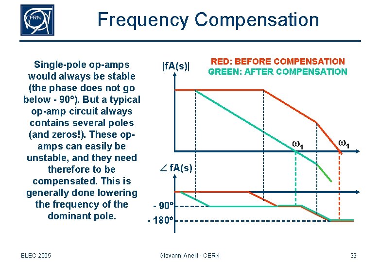
Frequency Compensation Single-pole op-amps |f. A(s)| would always be stable (the phase does not go below - 90 ). But a typical op-amp circuit always contains several poles (and zeros!). These opamps can easily be unstable, and they need f. A(s) therefore to be compensated. This is generally done lowering the frequency of the - 90 dominant pole. - 180 ELEC 2005 RED: BEFORE COMPENSATION GREEN: AFTER COMPENSATION Giovanni Anelli - CERN 33
Outline – Part II • • ELEC 2005 Noise in analog ICs Matching in analog ICs Operational Amplifier design examples Analog design methodology Giovanni Anelli - CERN 34
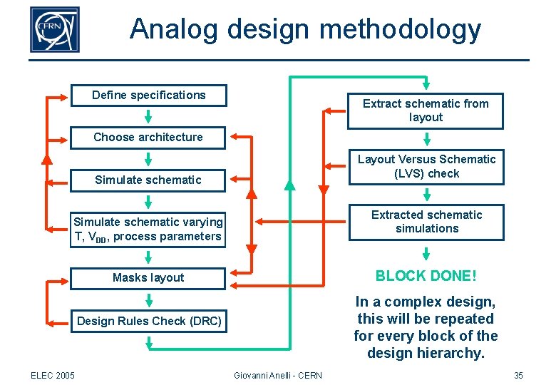
Analog design methodology Define specifications Extract schematic from layout Choose architecture Layout Versus Schematic (LVS) check Simulate schematic Extracted schematic simulations Simulate schematic varying T, VDD, process parameters BLOCK DONE! Masks layout In a complex design, this will be repeated for every block of the design hierarchy. Design Rules Check (DRC) ELEC 2005 Giovanni Anelli - CERN 35
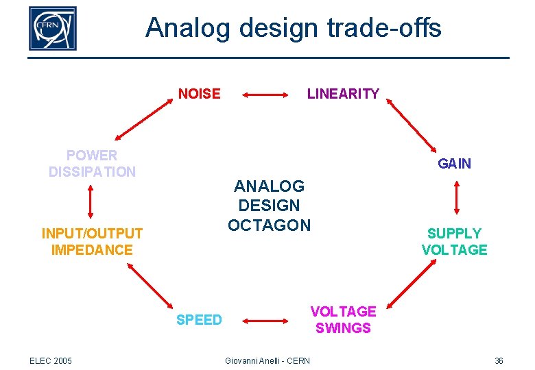
Analog design trade-offs NOISE POWER DISSIPATION LINEARITY GAIN ANALOG DESIGN OCTAGON INPUT/OUTPUT IMPEDANCE VOLTAGE SWINGS SPEED ELEC 2005 SUPPLY VOLTAGE Giovanni Anelli - CERN 36
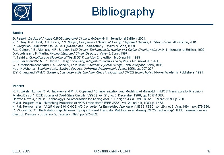
Bibliography Books: B. Razavi, Design of Analog CMOS Integrated Circuits, Mc. Graw-Hill International Edition, 2001. P. R. Gray, P. J. Hurst, S. H. Lewis, R. G. Meyer, Analysis and Design of Analog Integrated Circuits, J. Wiley & Sons, 4 th edition, 2001. R. Gregorian, Introduction to CMOS Op-Amps and Comparators, J. Wiley & Sons, 1999. R. L. Geiger, P. E. Allen and N. R. Strader, VLSI Design Techniques for Analog and Digital Circuits, Mc. Graw-Hill International Edition, 1990. D. A. Johns and K. Martin, Analog Integrated Circuit Design, J. Wiley & Sons, 1997. Y. Tsividis, Operation and Modeling of The MOS Transistor, 2 nd edition, Mc. Graw-Hill, 1999. K. R. Laker and W. M. C. Sansen, Design of Analog Integrated Circuits and Systems, Mc. Graw-Hill, 1994. C. D. Motchenbacher and J. A. Connelly, Low Noise Electronic System Design, John Wiley and Sons, 1993. A. L. Mc. Whorter, Semiconductor Surface Physics, University Pennsylvania Press, 1956, pp. 207 -227. Z. Y. Chang and W. M. C. Sansen, Low-noise wide-band amplifiers in bipolar and CMOS technologies, Kluwer Academic Publishers, 1991. Papers: K. R. Lakshmikumar, R. A. Hadaway and M. A. Copeland, "Characterization and Modeling of Mismatch in MOS Transistors for Precision Analog Design", IEEE Journal of Solid-State Circuits (JSSC), vol. 21, no. 6, December 1986, pp. 1057 -1066. Behzad Razavi, “CMOS Technology Characterization for Analog and RF Design", JSSC, vol. 34, no. 3, March 1999, p. 268. M. J. M. Pelgrom et al. , “Matching Properties of MOS Transistors”, IEEE JSSC, vol. 24, no. 10, 1989, p. 1433. M. J. M. Pelgrom et al. , “A 25 -Ms/s 8 -bit CMOS A/D Converter for Embedded Application”, IEEE JSSC, vol. 29, no. 8, Aug. 1994 , pp. 879 -886. R. W. Gregor, "On the Relationship Between Topography and Transistor Matching in an Analog CMOS Technology", IEEE Transactions on Electron Devices, vol. 39, no. 2, February 1992, pp. 275 -282. ELEC 2005 Giovanni Anelli - CERN 37
CERN Technical Training 2005 ELEC-2005 Electronics in High Energy Physics Spring term: Integrated circuits and VLSI technology for physics Basic Analog Design Giovanni Anelli 15 March 2005 Part II ELEC 2005 Giovanni Anelli - CERN