CERN Technical Training 2005 ELEC2005 Electronics in High

- Slides: 40
CERN Technical Training 2005 ELEC-2005 Electronics in High Energy Physics Spring term: Integrated circuits and VLSI technology for physics Basic Analog Design Giovanni Anelli 15 March 2005 Part I ELEC 2005 Giovanni Anelli - CERN
Outline – Part I • The MOS transistor: quick summary Ø The MOS transistor Ø DC characteristics Ø Important formulas • Basic analog building blocks ELEC 2005 Giovanni Anelli - CERN 2
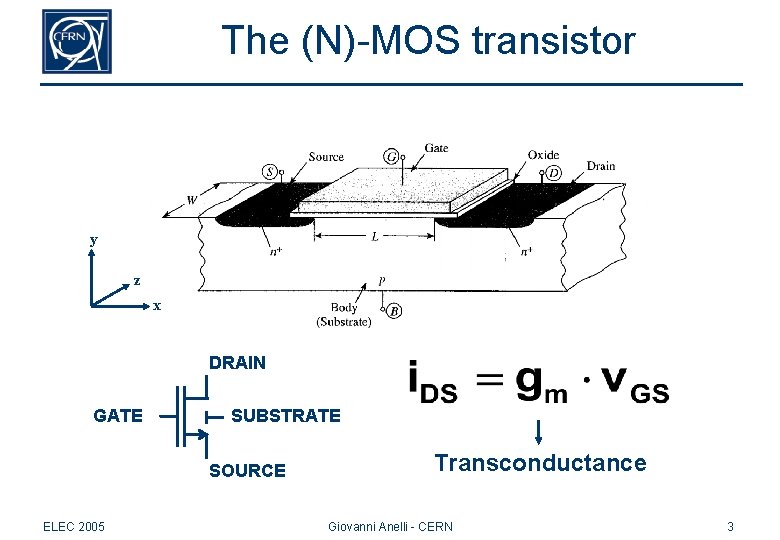
The (N)-MOS transistor y z x DRAIN GATE SUBSTRATE SOURCE ELEC 2005 Transconductance Giovanni Anelli - CERN 3
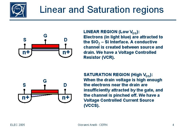
Linear and Saturation regions S G n+ S n+ ELEC 2005 D n+ G D n+ LINEAR REGION (Low VDS): Electrons (in light blue) are attracted to the Si. O 2 – Si Interface. A conductive channel is created between source and drain. We have a Voltage Controlled Resistor (VCR). SATURATION REGION (High VDS): When the drain voltage is high enough the electrons near the drain are insufficiently attracted by the gate, and the channel is pinched off. We have a Voltage Controlled Current Source (VCCS). Giovanni Anelli - CERN 4
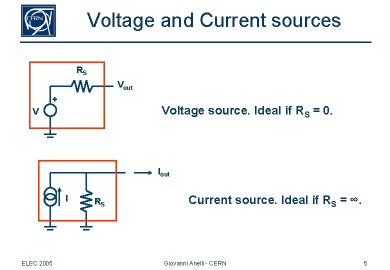
Voltage and Current sources RS Vout + Voltage source. Ideal if RS = 0. V Iout I ELEC 2005 RS Current source. Ideal if RS = ∞. Giovanni Anelli - CERN 5
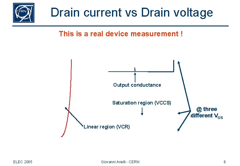
Drain current vs Drain voltage This is a real device measurement ! Output conductance Saturation region (VCCS) @ three different VGS Linear region (VCR) ELEC 2005 Giovanni Anelli - CERN 6
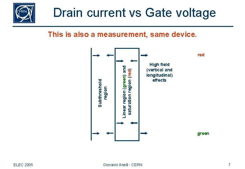
Drain current vs Gate voltage This is also a measurement, same device. Linear region (green) and saturation region (red) Subthreshold region red High field (vertical and longitudinal) effects green ELEC 2005 Giovanni Anelli - CERN 7
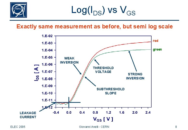
Log(IDS) vs VGS Exactly same measurement as before, but semi log scale red green WEAK INVERSION THRESHOLD VOLTAGE STRONG INVERSION SUBTHRESHOLD SLOPE LEAKAGE CURRENT ELEC 2005 Giovanni Anelli - CERN 8
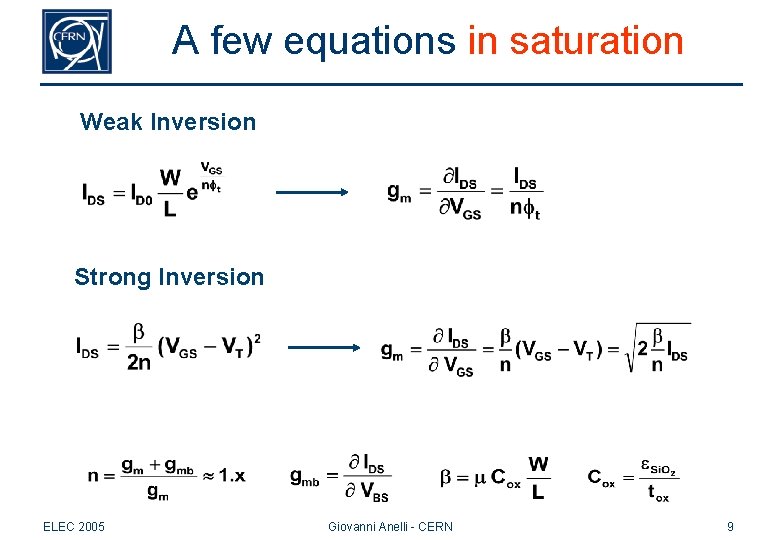
A few equations in saturation Weak Inversion Strong Inversion ELEC 2005 Giovanni Anelli - CERN 9
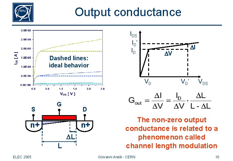
Output conductance IDS ID’ ID DV Dashed lines: ideal behavior VD S G n+ DL ELEC 2005 VD’ VDS D n+ L DI The non-zero output conductance is related to a phenomenon called channel length modulation Giovanni Anelli - CERN 10
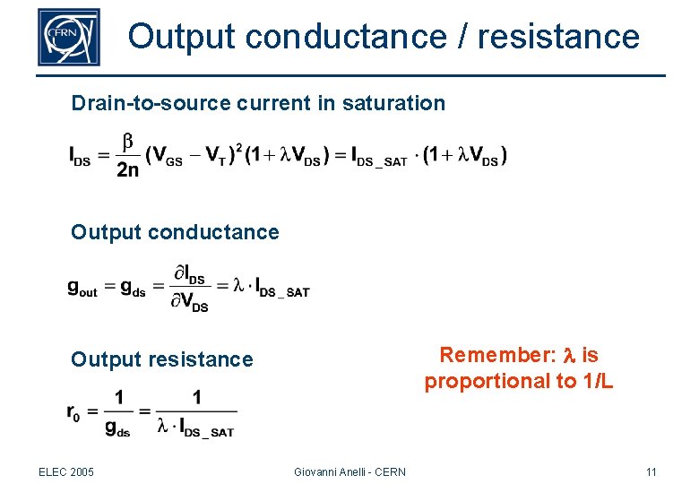
Output conductance / resistance Drain-to-source current in saturation Output conductance Remember: l is proportional to 1/L Output resistance ELEC 2005 Giovanni Anelli - CERN 11
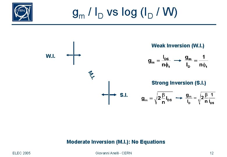
gm / ID vs log (ID / W) Weak Inversion (W. I. ) W. I. M. I. Strong Inversion (S. I. ) S. I. Moderate Inversion (M. I. ): No Equations ELEC 2005 Giovanni Anelli - CERN 12
Outline – Part I • The MOS transistor: quick summary • Basic analog building blocks Ø Ø Ø Ø ELEC 2005 Small-signal equivalent circuit Common-Source Stage Common-Gate Stage Cascode Stage Differential Pair Current Mirrors Differential Pair + Current Mirror Giovanni Anelli - CERN 13
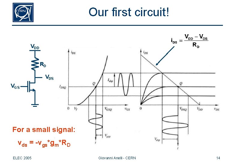
Our first circuit! VDD RD VDS VGS For a small signal: vds = -vgs*gm*RD ELEC 2005 Giovanni Anelli - CERN 14
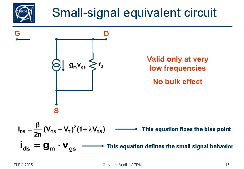
Small-signal equivalent circuit G D Valid only at very low frequencies No bulk effect S This equation fixes the bias point This equation defines the small signal behavior ELEC 2005 Giovanni Anelli - CERN 15
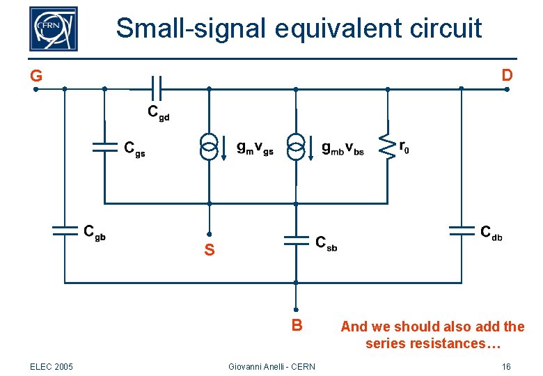
Small-signal equivalent circuit D G S B ELEC 2005 Giovanni Anelli - CERN And we should also add the series resistances… 16
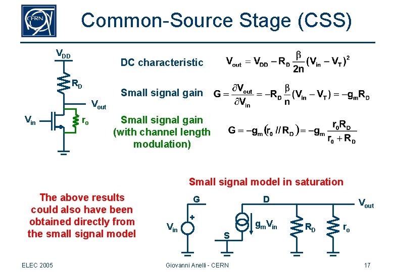
Common-Source Stage (CSS) VDD DC characteristic RD Small signal gain Vout Vin ro Small signal gain (with channel length modulation) Small signal model in saturation The above results could also have been obtained directly from the small signal model ELEC 2005 G Vin D + gm. Vin S Giovanni Anelli - CERN Vout RD ro 17
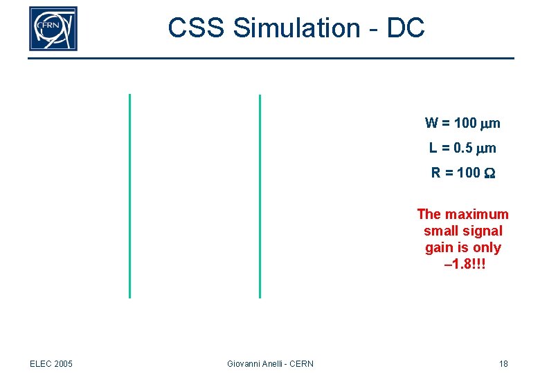
CSS Simulation - DC W = 100 mm L = 0. 5 mm R = 100 W The maximum small signal gain is only – 1. 8!!! ELEC 2005 Giovanni Anelli - CERN 18
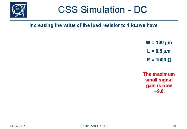
CSS Simulation - DC Increasing the value of the load resistor to 1 k. W we have W = 100 mm L = 0. 5 mm R = 1000 W The maximum small signal gain is now – 9. 6. ELEC 2005 Giovanni Anelli - CERN 19
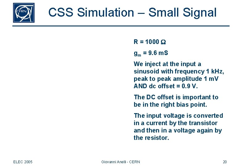
CSS Simulation – Small Signal R = 1000 W gm = 9. 6 m. S We inject at the input a sinusoid with frequency 1 k. Hz, peak to peak amplitude 1 m. V AND dc offset = 0. 9 V. The DC offset is important to be in the right bias point. The input voltage is converted in a current by the transistor and then in a voltage again by the resistor. ELEC 2005 Giovanni Anelli - CERN 20
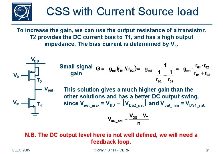
CSS with Current Source load To increase the gain, we can use the output resistance of a transistor. T 2 provides the DC current bias to T 1, and has a high output impedance. The bias current is determined by Vb. VDD Small signal gain Vb T 2 Vout Vin T 1 This solution gives a much higher gain than the other solutions and has a better DC output swing, since Vout_max = VDD – VDS 2_sat and Vout_min = VDS 1_sat. N. B. The DC output level here is not well defined, we will need a feedback loop. ELEC 2005 Giovanni Anelli - CERN 21
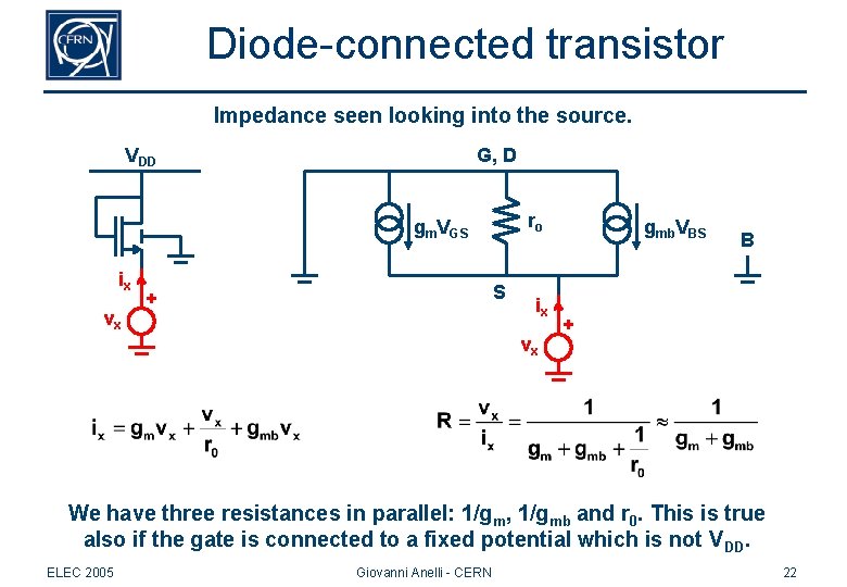
Diode-connected transistor Impedance seen looking into the source. VDD G, D ro gm. VGS ix vx S + ix vx gmb. VBS B + We have three resistances in parallel: 1/gm, 1/gmb and r 0. This is true also if the gate is connected to a fixed potential which is not V DD. ELEC 2005 Giovanni Anelli - CERN 22
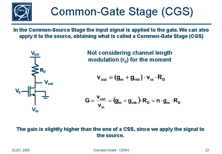
Common-Gate Stage (CGS) In the Common-Source Stage the input signal is applied to the gate. We can also apply it to the source, obtaining what is called a Common-Gate Stage (CGS) Not considering channel length modulation (r 0) for the moment VDD RD Vout Vb Vin The gain is slightly higher than the one of a CSS, since we apply the signal to the source. ELEC 2005 Giovanni Anelli - CERN 23
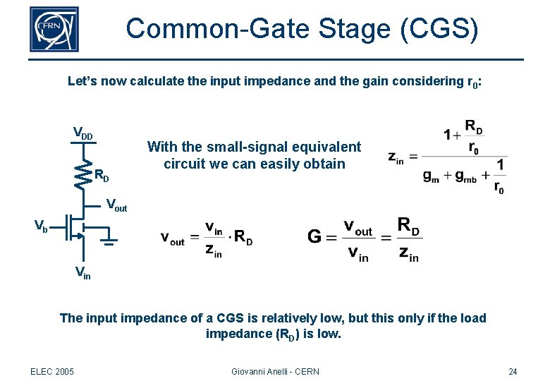
Common-Gate Stage (CGS) Let’s now calculate the input impedance and the gain considering r 0: VDD RD With the small-signal equivalent circuit we can easily obtain Vout Vb Vin The input impedance of a CGS is relatively low, but this only if the load impedance (RD) is low. ELEC 2005 Giovanni Anelli - CERN 24
Cascode Stage (Casc. S) The “cascade” of a Common-Source Stage (V-I converter) and of a Common-Gate Stage is called a “Cascode”. VDD REMINDER I RD Vout R 1 R 2 T 2 Vb r 01 Vin T 1 ELEC 2005 The gain is practically the same as in the case of a Common-Source Stage. Giovanni Anelli - CERN 25
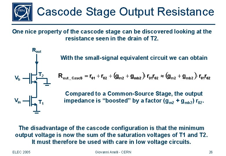
Cascode Stage Output Resistance One nice property of the cascode stage can be discovered looking at the resistance seen in the drain of T 2. Rout With the small-signal equivalent circuit we can obtain Vb Vin T 2 T 1 Compared to a Common-Source Stage, the output impedance is “boosted” by a factor (gm 2 + gmb 2) r 02. The disadvantage of the cascode configuration is that the minimum output voltage is now the sum of the saturation voltages of T 1 and T 2. It must therefore be used with care in low voltage circuits. ELEC 2005 Giovanni Anelli - CERN 26
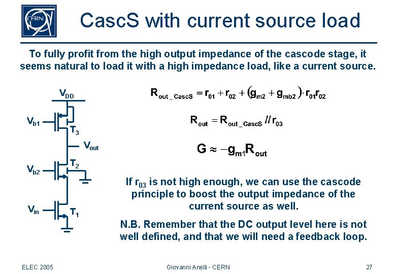
Casc. S with current source load To fully profit from the high output impedance of the cascode stage, it seems natural to load it with a high impedance load, like a current source. VDD Vb 1 T 3 Vout Vb 2 Vin T 2 T 1 If r 03 is not high enough, we can use the cascode principle to boost the output impedance of the current source as well. N. B. Remember that the DC output level here is not well defined, and that we will need a feedback loop. ELEC 2005 Giovanni Anelli - CERN 27
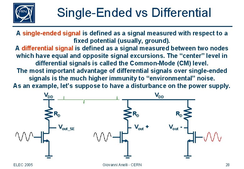
Single-Ended vs Differential A single-ended signal is defined as a signal measured with respect to a fixed potential (usually, ground). A differential signal is defined as a signal measured between two nodes which have equal and opposite signal excursions. The “center” level in differential signals is called the Common-Mode (CM) level. The most important advantage of differential signals over single-ended signals is the much higher immunity to “environmental” noise. As an example, let’s suppose to have a disturbance on the power supply. VDD RD Vout_SE ELEC 2005 RD Vout + Giovanni Anelli - CERN RD Vout - 28
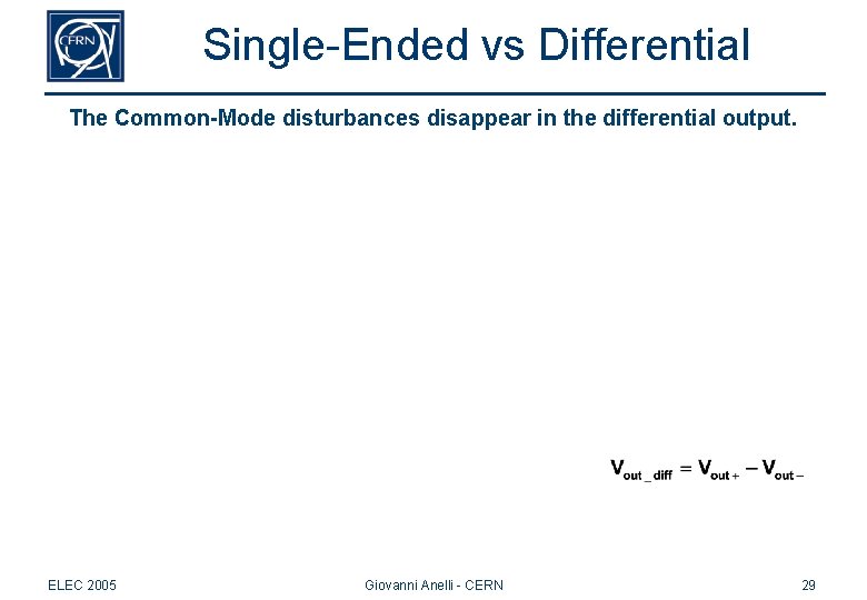
Single-Ended vs Differential The Common-Mode disturbances disappear in the differential output. ELEC 2005 Giovanni Anelli - CERN 29
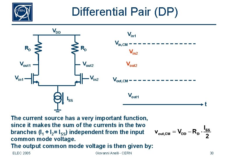
Differential Pair (DP) VDD Vin 1 RD Vin, CM RD Vout 1 Vin 2 Vout 2 Vin 1 Vin 2 ISS Vout, CM Vout 1 t The current source has a very important function, since it makes the sum of the currents in the two branches (I 1 + I 2= ISS) independent from the input common mode voltage. The output common mode voltage is then given by: ELEC 2005 Giovanni Anelli - CERN 30
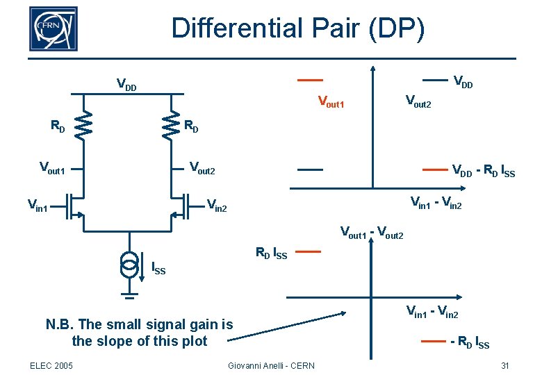
Differential Pair (DP) VDD Vout 1 RD Vout 2 RD Vout 1 Vout 2 Vin 1 VDD - RD ISS Vin 1 - Vin 2 Vout 1 - Vout 2 RD ISS N. B. The small signal gain is the slope of this plot ELEC 2005 Giovanni Anelli - CERN Vin 1 - Vin 2 - RD ISS 31
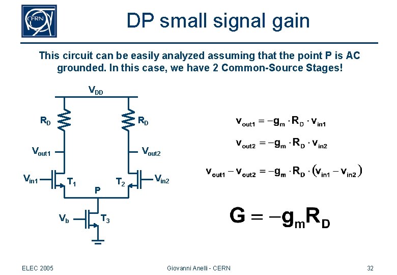
DP small signal gain This circuit can be easily analyzed assuming that the point P is AC grounded. In this case, we have 2 Common-Source Stages! VDD RD RD Vout 1 Vin 1 Vout 2 T 1 Vb ELEC 2005 T 2 P Vin 2 T 3 Giovanni Anelli - CERN 32
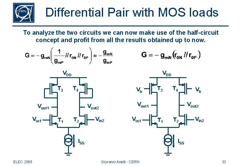
Differential Pair with MOS loads To analyze the two circuits we can now make use of the half-circuit concept and profit from all the results obtained up to now. VDD T 3 VDD T 4 T 1 T 2 Vin 1 ISS ELEC 2005 T 3 T 4 Vb Vout 2 Vout 1 Vin 1 Vb T 1 T 2 Vin 2 ISS Giovanni Anelli - CERN 33
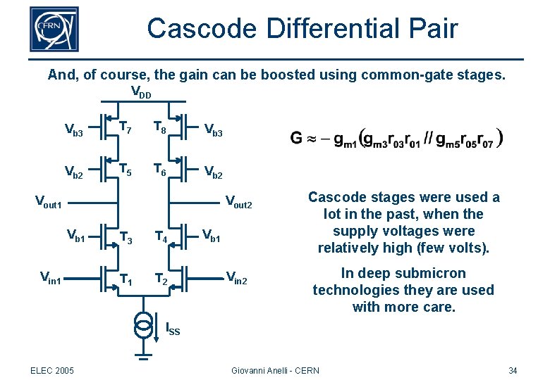
Cascode Differential Pair And, of course, the gain can be boosted using common-gate stages. VDD Vb 3 T 7 T 8 Vb 3 Vb 2 T 5 T 6 Vb 2 Vout 1 Vb 1 Vin 1 T 3 T 4 T 1 T 2 Vout 2 Cascode stages were used a lot in the past, when the supply voltages were relatively high (few volts). Vin 2 In deep submicron technologies they are used with more care. Vb 1 ISS ELEC 2005 Giovanni Anelli - CERN 34
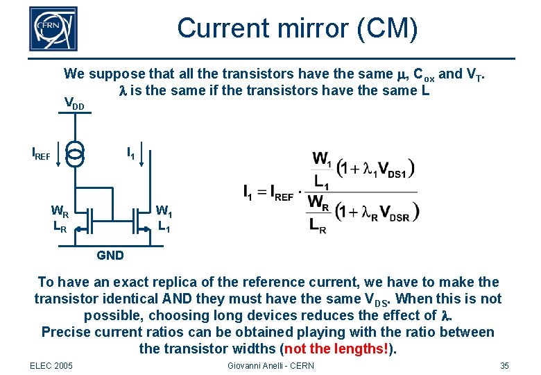
Current mirror (CM) We suppose that all the transistors have the same m, Cox and VT. l is the same if the transistors have the same L VDD IREF I 1 WR LR W 1 L 1 GND To have an exact replica of the reference current, we have to make the transistor identical AND they must have the same VDS. When this is not possible, choosing long devices reduces the effect of l. Precise current ratios can be obtained playing with the ratio between the transistor widths (not the lengths!). ELEC 2005 Giovanni Anelli - CERN 35
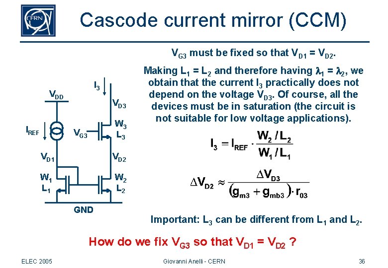
Cascode current mirror (CCM) VG 3 must be fixed so that VD 1 = VD 2. I 3 VDD IREF VD 3 W 3 L 3 VG 3 VD 1 VD 2 W 1 L 1 W 2 L 2 GND Making L 1 = L 2 and therefore having l 1 = l 2, we obtain that the current I 3 practically does not depend on the voltage VD 3. Of course, all the devices must be in saturation (the circuit is not suitable for low voltage applications). Important: L 3 can be different from L 1 and L 2. How do we fix VG 3 so that VD 1 = VD 2 ? ELEC 2005 Giovanni Anelli - CERN 36
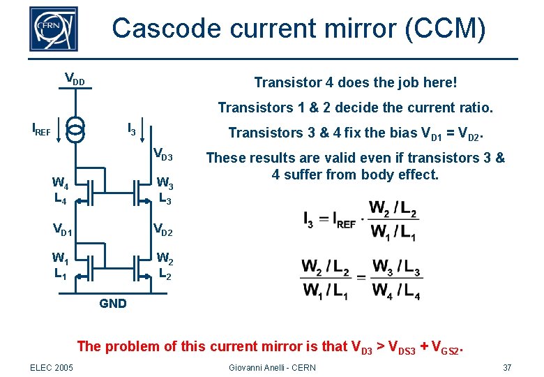
Cascode current mirror (CCM) VDD Transistor 4 does the job here! Transistors 1 & 2 decide the current ratio. IREF I 3 Transistors 3 & 4 fix the bias VD 1 = VD 2. VD 3 W 4 L 4 W 3 L 3 VD 1 VD 2 W 1 L 1 W 2 L 2 These results are valid even if transistors 3 & 4 suffer from body effect. GND The problem of this current mirror is that VD 3 > VDS 3 + VGS 2. ELEC 2005 Giovanni Anelli - CERN 37
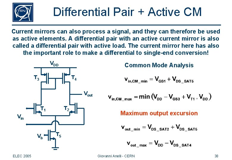
Differential Pair + Active CM Current mirrors can also process a signal, and they can therefore be used as active elements. A differential pair with an active current mirror is also called a differential pair with active load. The current mirror here has also the important role to make a differential to single-end conversion! VDD Common Mode Analysis T 3 T 4 Vout T 2 T 1 Vin Vb ELEC 2005 Maximum output excursion T 5 Giovanni Anelli - CERN 38
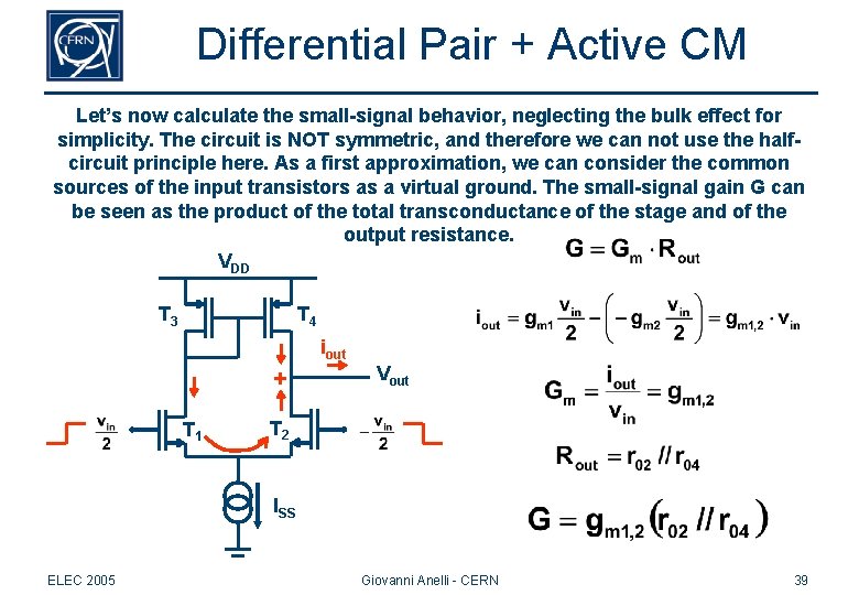
Differential Pair + Active CM Let’s now calculate the small-signal behavior, neglecting the bulk effect for simplicity. The circuit is NOT symmetric, and therefore we can not use the halfcircuit principle here. As a first approximation, we can consider the common sources of the input transistors as a virtual ground. The small-signal gain G can be seen as the product of the total transconductance of the stage and of the output resistance. VDD T 3 T 4 iout + T 1 Vout T 2 ISS ELEC 2005 Giovanni Anelli - CERN 39
CERN Technical Training 2005 ELEC-2005 Electronics in High Energy Physics Spring term: Integrated circuits and VLSI technology for physics Basic Analog Design Giovanni Anelli 15 March 2005 Part I ELEC 2005 Giovanni Anelli - CERN