Feedback Amplifiers Outline Introduction The general feedback structure

Feedback Amplifiers

Outline • • Introduction The general feedback structure Some properties of negative feedback The four basic feedback topologies The series-shunt feedback amplifier The series-series feedback amplifier The shunt-shunt and shunt-series feedback amplifier

• The stability problem • Stability study using bode plot • Frequency compensation

Introduction • It’s impossible to think of electronic circuits without some forms of feedback. • Negative feedback ØDesensitize the gain ØReduce nonlinear distortion ØReduce the effect of noise ØControl the input and output impedance ØExtend the bandwidth of the amplifier

• The basic idea of negative feedback is to trade off gain for other desirable properties. • Positive feedback will cause the amplifier oscillation.

The General Feedback Structure This is a signal-flow diagram, and the quantities x represent either voltage or current signals.

The General Feedback Equation • Closed loop and open loop • Closed loop gain • Feedback factor β • Loop gain Aβ • Amount of feedback (1+ Aβ)

Some Properties of Negative Feedback • Gain desensitivity • Bandwidth extension • Noise reduction • Reduction in nonlinear distortion

The Four Basic Feedback Topologies • Voltage amplifier---series-shunt feedback voltage mixing and voltage sampling • Current amplifier---shunt-series feedback Current mixing and current sampling

• Transconducatnce amplifier---series feedback Voltage mixing and current sampling • Transresistance amplifier---shunt feedback Current mixing and voltage sampling
 topology")
The Series-Shunt Feedback Topologies voltage-mixing voltage-sampling (series– shunt) topology
 topology")
The Amplifier with Series-Shunt Feedback voltage-mixing voltage-sampling (series– shunt) topology
 topology")
The Shunt-Series Feedback Topologies current-mixing current-sampling (shunt– series) topology
 topology")
The Amplifier with Shunt-Series Feedback current-mixing current-sampling (shunt– series) topology
 topology")
The Series-Series Feedback Topologies voltage-mixing current-sampling (series– series) topology
 topology")
The Amplifier with Series-Series Feedback voltage-mixing current-sampling (series– series) topology
 topology")
The Shunt-Shunt Feedback Topologies current-mixing voltage-sampling (shunt– shunt) topology
 topology")
The OP Amplifier with Shunt-Shunt Feedback current-mixing voltage-sampling (shunt– shunt) topology

The Series-Shunt Feedback Amplifier • The ideal situation • The practical situation • summary

The Ideal Situation
. ØAn ideal voltage mixing voltage sampling feedback network")
ØA unilateral open-loop amplifier (A circuit). ØAn ideal voltage mixing voltage sampling feedback network (β circuit). ØAssumption that the source and load resistance have been included inside the A circuit.

The Ideal Situation Equivalent circuit. Rif and Rof denote the input and output resistance with feedback.

Input and Output Resistance with Feedback • Input resistance In this case, the negative feedback increases the input resistance by a factor equal to the amount of feedback.

• Output resistance In this case, the negative feedback reduces the output resistance by a factor equal to the amount of feedback.

The Practical Situation ØBlock diagram of a practical series–shunt feedback amplifier. ØFeedback network is not ideal and load the basic amplifier thus affect the values of gain, input resistance and output resistance.
 with the feedback network represented by its")
The Practical Situation The circuit in (a) with the feedback network represented by its h parameters.
 with h 21 neglected.")
The Practical Situation The circuit in (b) with h 21 neglected.

The Practical Situation • The load effect of the feedback network on the basic amplifier is represented by the components h 11 and h 22. • The loading effect is found by looking into the appropriate port of the feedback network while the port is open-circuit or short-circuit so as to destroy the feedback.

• If the connection is a shunt one, shortcircuit the port. • If the connection is a series one, opencircuit the port. • Determine the β.
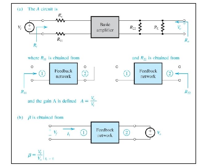

Summary • Ri and Ro are the input and output resistances, respectively, of the A circuit. • Rif and Rof are the input and output resistances, respectively, of the feedback amplifier, including Rs and RL. • The actual input and output resistances exclude Rs and RL.

Example of Series-Shunt Feedback Amplifier

Example of Series-Shunt Feedback Amplifier • Op amplifier connected in noninverting configuration with the open-loop gain μ, Rid and ro • Find expression for A, β, the closed-loop gain Vo/Vi , the input resistance Rin and the output resistance Rout • Find numerical values

Example of Series-Shunt Feedback Amplifier

Example of Series-Shunt Feedback Amplifier

The Series-Series Feedback Amplifier • The ideal situation • The practical situation • summary

The Ideal Situation Trans conductance gain

The Ideal Situation Tranresistance feedback factor

Input and Output Resistance with Feedback • Input resistance In this case, the negative feedback increases the input resistance by a factor equal to the amount of feedback.

• Output resistance In this case, the negative feedback increases the output resistance by a factor equal to the amount of feedback.

The Practical Situation Block diagram of a practical series–series feedback amplifier.

• Feedback network is not ideal and load the basic amplifier thus affect the values of gain, input resistance and output resistance.
 with the feedback network represented by its")
The Practical Situation The circuit of (a) with the feedback network represented by its z parameters.
 with z 21 neglected.")
The Practical Situation A redrawing of the circuit in (b) with z 21 neglected.

The Practical Situation • The load effect of the feedback network on the basic amplifier is represented by the components Z 11 and Z 22. • Z 11 is the impedance looking into port 1 of the feedback network with port 2 opencircuited.

• Z 22 is the impedance looking into port 2 of the feedback network with port 1 open-circuited. • Determine the β.
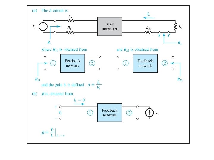

Summary • Ri and Ro are the input and output resistances, respectively, of the A circuit. • Rif and Rof are the input and output resistances, respectively, of the feedback amplifier, including Rs and RL.

• The actual input and output resistances exclude Rs and RL.

Example of Series-Series Feedback Amplifier

Example of Series-Series Feedback Amplifier

Example of Series-Series Feedback Amplifier

Example of Series-Series Feedback Amplifier

The Shunt-Shunt and Shunt-Series Feedback Amplifiers • Study by yourselves • Important notes: ØClosed-loop gain ØFeedback factor ØLoad effect ØSummary Øexample

The Stability Problem • Closed-loop transfer function is similar to the one of the middle band gain. • The condition for negative feedback to oscillate

• Any right-half-plane poles results in instability. ØAmplifier with a single-pole is unconditionally stable. ØAmplifier with two-pole is also unconditionally stable. ØAmplifier with more than two poles has the possibility to be unstable. • Stability study using bode plot

The Definitions of the Gain and Phase margins

ØGain margin represents the amount by which the loop gain can be increased while stability is maintained. ØUnstable and oscillatory ØStable and non-oscillatory ØOnly when the phase margin exceed 45º or gain margin exceed 6 d. B, can the amplifier be stable.

Stability analysis using Bode plot of |A|

Stability Analysis Using Bode Plot of |A| • Gain margin and phase margin • The horizontal line of inverse of feedback factor in d. B. • A rule of thumb: The closed-loop amplifier will be stable if the 20 log(1/β) line intersects the 20 log|A| curve at a point on the – 20 d. B/decade segment.

• The general rule states: At the intersection of 20 log[1/ | β (jω)| ] and 20 log |A(jω)| the difference of slopes should not exceed 20 d. B/decade.

Frequency Compensation • The purpose is to modifying the open-loop transfer function of an amplifier having three or more poles so that the closed-loop amplifier is stable for any desired value of closed-loop gain. • Theory of frequency compensation is the enlarge the – 20 d. B/decade line.

• Implementation ØCapacitance Cc added ØMiller compensation and pole splitting

Frequency Compensation

• Two cascaded gain multistage amplifier. stages of a • Equivalent circuit for the interface between the two stages in (a). • Same circuit as in (b) but with a compensating capacitor CC added.
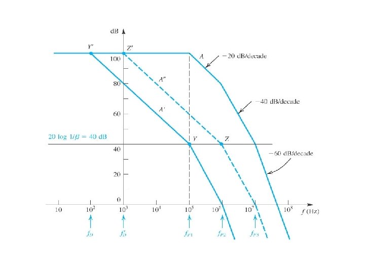

• Frequency compensation for b = 10 -2. The response labeled A¢ is obtained by introducing an additional pole at f. D. The A² response is obtained by moving the original low-frequency pole to f ¢D.

Frequency Compensation ØA gain stage in a multistage amplifier with a compensating capacitor connected in the feedback path ØAn equivalent circuit.
- Slides: 68