CMOS Process Flow 1 Wafer Selection and Cleaning


 1 2 3")
 1 Removal of Gate Oxide Layer 4 2 Gate")


 Very high temperature then cooling to relax the")


 7 Vth Adjustment (Field Implant) 8 Polysilicon Deposition")
")
- Slides: 17
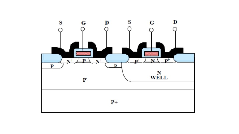
CMOS Process Flow
1 - Wafer Selection and Cleaning
2 - Active Region Formation LOCOS Process 1 4 2 5 3 6
2 - Active Region Formation LOCOS Process 7 8 9
3 - N and P Well Formation 1 2 3 Done in 2 ways 4
4 - Vth Adjustment (Field Implant) 1 2 3
5 - Polysilicon Formation (Gate) 1 Removal of Gate Oxide Layer 4 2 Gate Oxide Re-growth 3 Deposition of Polysilicon Electrode Polysilicon Etching Why did we leave the Si. O 2 from the beginning? To avoid channeling The Si. O 2 atoms are amorphous so the ions are randomized and stop when they hit an atom. The P- type silicon is single crystalline.
6 - Lightly Doped Drain 1 N+ N- P instead of N+ P to avoid high electric field between N+ and P 2 Self Alignment The polysilicon gate is used to align the drain and source without using a mask
Formation of Sidewall Spacer 2 1 3 Deposition of “Screen” Oxide Layer
7 - Formation of Source and Drain 1 2
8 - Annealing (Drive in Process) Very high temperature then cooling to relax the bonds in the material 1 2
9 - Metal Interconnect 1 4 Titanium and N+ form titanium-silica which is a very good conductor 2 Ti 5 Titanium and Nitrogen form titaniumnitride which is also a conductor 3 N 2 6 Planarization by Chemical Mechanical Polishing (CMP)
9 - Metal Interconnect 7 Open holes for via 8 Why is the annealing done before the metal interconnect? Because the metal will melt
1 2 A heavily doped P substrate is chosen A lightly doped layer is grown on top 3 Active Region Formation (LOCOS) and P implant 4 N well Formation High Temperature to complete N well Formation
5 6 Vth Adjustment (Field Implant) 7 Vth Adjustment (Field Implant) 8 Polysilicon Deposition
10 9 Gates 11 Source and Drain Formation (Self Alignment)