Dynamic Logic Circuits Dynamic logic is temporary transient
- Slides: 34

Dynamic Logic Circuits * • Dynamic logic is temporary (transient) in that output levels will remain valid only for a certain period of time – Static logic retains its output level as long as power is applied • Dynamic logic is normally done with charging and selectively discharging capacitance (i. e. capacitive circuit nodes) – Precharge clock to charge the capacitance – Evaluate clock to discharge the capacitance depending on condition of logic inputs • Advantages over static logic: – – – Avoids duplicating logic twice as both N-tree and P-tree, as in standard CMOS Typically can be used in very high performance applications Very simple sequential memory circuits; amenable to synchronous logic High density achievable Consumes less power (in some cases) • Disadvantages compared to static logic: – Problems with clock synchronization and timing – Design is more difficult * Kang and Leblebicic, chapter 9 R. W. Knepper SC 571, page 5 -55

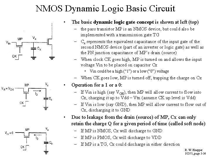
NMOS Dynamic Logic Basic Circuit • The basic dynamic logic gate concept is shown at left (top) – the pass transistor MP is an NMOS device, but could also be implemented with a transmission gate TG – Cx represents the equivalent capacitance of the input gate of the second NMOS device (part of an inverter or logic gate) as well as the PN junction capacitance of MP’s drain (source) – When clock CK goes high, MP is turned on and allows the input voltage Vin to be placed on capacitor Cx • Vin could be a high (“ 1”) or a low (“ 0”) voltage – When CK goes low, MP is turned off, trapping the charge on Cx • Operation for a 1 or a 0: – If Vin is high (say VOH), then MP will allow current to flow into Cx, charging it up to Vdd – Vtn (assume CK up level is Vdd) – If Vin is low (say GND), then MP will allow current to flow out of Cx, discharging it to GND • Due to leakage from the drain (source) of MP, Cx can only retain the charge Q for a given period of time (called soft node) – If MP is NMOS, Cx will discharge to GND – If MP is PMOS, Cx will discharge to VDD – If MP is a TG, Cx could discharge in either direction R. W. Knepper SC 571, page 5 -56

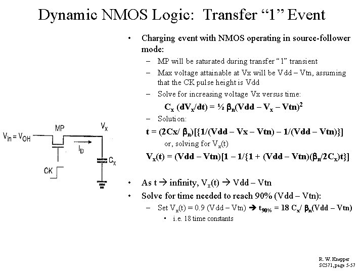
Dynamic NMOS Logic: Transfer “ 1” Event • Charging event with NMOS operating in source-follower mode: – MP will be saturated during transfer “ 1” transient – Max voltage attainable at Vx will be Vdd – Vtn, assuming that the CK pulse height is Vdd – Solve for increasing voltage Vx versus time: Cx (d. Vx/dt) = ½ n(Vdd – Vx – Vtn)2 – Solution: t = (2 Cx/ n)[{1/(Vdd – Vx – Vtn) – 1/(Vdd – Vtn)}] or, solving for Vx(t) = (Vdd – Vtn)[1 – 1/{1 + (Vdd – Vtn)( n/2 Cx)t}] • • As t infinity, Vx(t) Vdd – Vtn Solve for time needed to reach 90% (Vdd – Vtn): – Set Vx(t) = 0. 9 (Vdd – Vtn) t 90% = 18 Cx/ n(Vdd – Vtn) • i. e. 18 time constants R. W. Knepper SC 571, page 5 -57

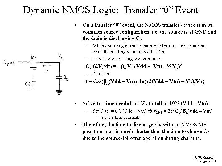
Dynamic NMOS Logic: Transfer “ 0” Event • On a transfer “ 0” event, the NMOS transfer device is in its common source configuration, i. e. the source is at GND and the drain is discharging Cx – MP is operating in the linear mode for the entire transient since the starting value is Vdd – Vtn – Solve for decreasing Vx with time: Cx (d. Vx/dt) = - n Vx (Vdd – Vtn - ½ Vx)2 – Solution: t = Cx/( n(Vdd – Vtn)) ln{(2(Vdd – Vtn) – Vx)/Vx} • Solve for time needed for Vx to fall to 10% (Vdd – Vtn): – Set Vx(t) = 0. 1 (Vdd – Vtn) t 10% = 2. 9 Cx/ n(Vdd – Vtn) • i. e. 2. 9 time constants • Therefore, the time to discharge Cx with an NMOS MP pass transistor is much shorter than the time to charge Cx due to the source-follower operation during charging. R. W. Knepper SC 571, page 5 -58

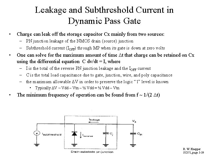
Leakage and Subthreshold Current in Dynamic Pass Gate • Charge can leak off the storage capacitor Cx mainly from two sources: – PN junction leakage of the NMOS drain (source) junction – Subthreshold current (IOFF) through MP when its gate is down at zero volts • One can solve for the maximum amount of time t that charge can be retained on Cx using the differential equation C dv/dt = I, where – I is the total of the reverse PN junction leakage and the IOFF current – C is the total load capacitance due to gate, junction, wire, and poly capacitance – the maximum allowable V in order to preserve the logic “ 1” level is known • Typically V ~ Vdd – Vtn – ½ Vdd = ½ Vdd – Vtn • The minimum frequency of operation can be found from f ~ 1/(2 t) R. W. Knepper SC 571, page 5 -59

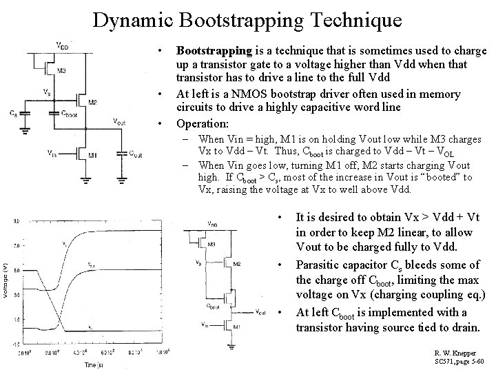
Dynamic Bootstrapping Technique • • • Bootstrapping is a technique that is sometimes used to charge up a transistor gate to a voltage higher than Vdd when that transistor has to drive a line to the full Vdd At left is a NMOS bootstrap driver often used in memory circuits to drive a highly capacitive word line Operation: – When Vin = high, M 1 is on holding Vout low while M 3 charges Vx to Vdd – Vt. Thus, Cboot is charged to Vdd – Vt – VOL – When Vin goes low, turning M 1 off, M 2 starts charging Vout high. If Cboot > Cs, most of the increase in Vout is “booted” to Vx, raising the voltage at Vx to well above Vdd. • • • It is desired to obtain Vx > Vdd + Vt in order to keep M 2 linear, to allow Vout to be charged fully to Vdd. Parasitic capacitor Cs bleeds some of the charge off Cboot, limiting the max voltage on Vx (charging coupling eq. ) At left Cboot is implemented with a transistor having source tied to drain. R. W. Knepper SC 571, page 5 -60

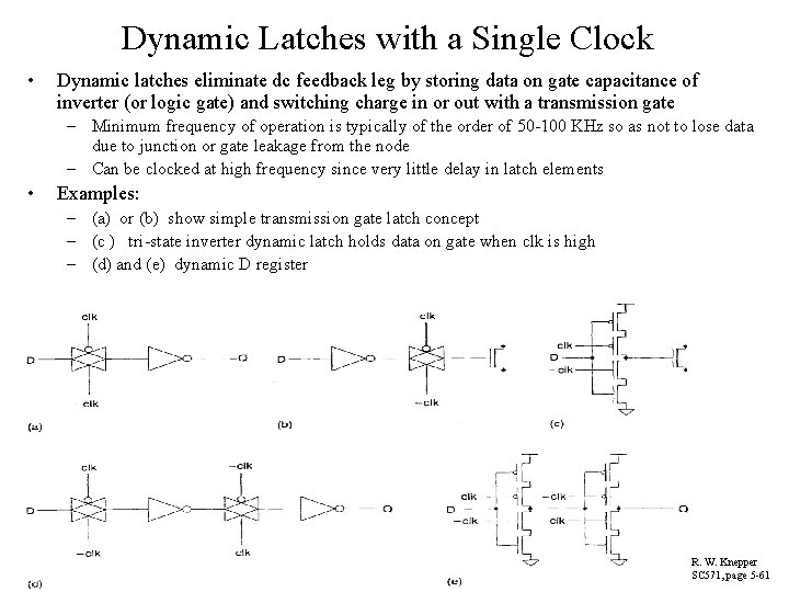
Dynamic Latches with a Single Clock • Dynamic latches eliminate dc feedback leg by storing data on gate capacitance of inverter (or logic gate) and switching charge in or out with a transmission gate – Minimum frequency of operation is typically of the order of 50 -100 KHz so as not to lose data due to junction or gate leakage from the node – Can be clocked at high frequency since very little delay in latch elements • Examples: – (a) or (b) show simple transmission gate latch concept – (c ) tri-state inverter dynamic latch holds data on gate when clk is high – (d) and (e) dynamic D register R. W. Knepper SC 571, page 5 -61

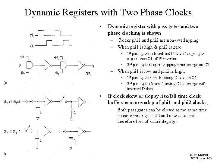
Dynamic Registers with Two Phase Clocks • Dynamic register with pass gates and two phase clocking is shown – Clocks phi 1 and phi 2 are non-overlapping – When phi 1 is high & phi 2 is zero, • 1 st pass gate is closed and D data charges gate capacitance C 1 of 1 st inverter • 2 nd pass gate is open trapping prior charge on C 2 – When phi 1 is low and phi 2 is high, • 1 st pass gate opens trapping D data on C 1 • 2 nd pass gate closes allowing C 2 to charge with inverted D data • If clock skew or sloppy rise/fall time clock buffers cause overlap of phi 1 and phi 2 clocks, – Both pass gates can be closed at the same time causing mixing of old and new data and therefore loss of data integrity! R. W. Knepper SC 571, page 5 -62

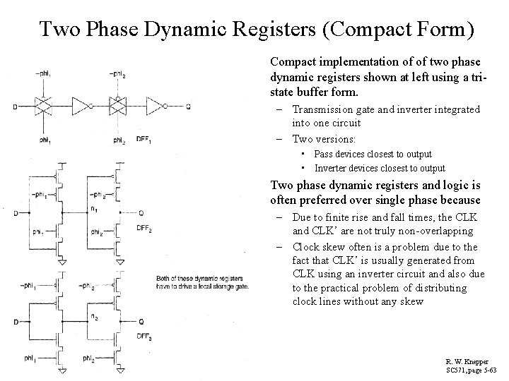
Two Phase Dynamic Registers (Compact Form) • Compact implementation of of two phase dynamic registers shown at left using a tristate buffer form. – Transmission gate and inverter integrated into one circuit – Two versions: • Pass devices closest to output • Inverter devices closest to output • Two phase dynamic registers and logic is often preferred over single phase because – Due to finite rise and fall times, the CLK and CLK’ are not truly non-overlapping – Clock skew often is a problem due to the fact that CLK’ is usually generated from CLK using an inverter circuit and also due to the practical problem of distributing clock lines without any skew R. W. Knepper SC 571, page 5 -63

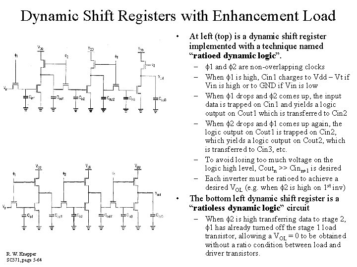
Dynamic Shift Registers with Enhancement Load • At left (top) is a dynamic shift register implemented with a technique named “ratioed dynamic logic”. – 1 and 2 are non-overlapping clocks – When 1 is high, Cin 1 charges to Vdd – Vt if Vin is high or to GND if Vin is low – When 1 drops and 2 comes up, the input data is trapped on Cin 1 and yields a logic output on Cout 1 which is transferred to Cin 2 – When 2 drops and 1 comes up again, the logic output on Cout 1 is trapped on Cin 2, which yields a logic output on Cout 2, which is transferred to Cin 3, etc. – To avoid losing too much voltage on the logic high level, Coutn >> Cinn+1 is desired – Each inverter must be ratioed to achieve a desired VOL (e. g. when 2 is high on 1 st inv) • R. W. Knepper SC 571, page 5 -64 The bottom left dynamic shift register is a “ratioless dynamic logic” circuit – When 2 is high transferring data to stage 2, 1 has already turned off the stage 1 load transistor, allowing a VOL = 0 to be obtained without a ratio condition between load and driver transistors.

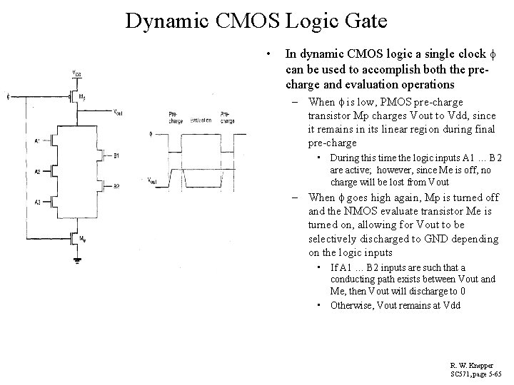
Dynamic CMOS Logic Gate • In dynamic CMOS logic a single clock can be used to accomplish both the precharge and evaluation operations – When is low, PMOS pre-charge transistor Mp charges Vout to Vdd, since it remains in its linear region during final pre-charge • During this time the logic inputs A 1 … B 2 are active; however, since Me is off, no charge will be lost from Vout – When goes high again, Mp is turned off and the NMOS evaluate transistor Me is turned on, allowing for Vout to be selectively discharged to GND depending on the logic inputs • If A 1 … B 2 inputs are such that a conducting path exists between Vout and Me, then Vout will discharge to 0 • Otherwise, Vout remains at Vdd R. W. Knepper SC 571, page 5 -65

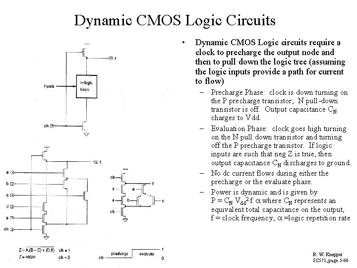
Dynamic CMOS Logic Circuits • Dynamic CMOS Logic circuits require a clock to precharge the output node and then to pull down the logic tree (assuming the logic inputs provide a path for current to flow) – Precharge Phase: clock is down turning on the P precharge transistor; N pull-down transistor is off. Output capacitance CN charges to Vdd. – Evaluation Phase: clock goes high turning on the N pull down transistor and turning off the P precharge transistor. If logic inputs are such that neg Z is true, then output capacitance CN discharges to ground. – No dc current flows during either the precharge or the evaluate phase. – Power is dynamic and is given by P = CN Vdd 2 f where CN represents an equivalent total capacitance on the output, f = clock frequency, =logic repetition rate R. W. Knepper SC 571, page 5 -66

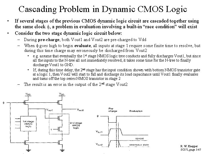
Cascading Problem in Dynamic CMOS Logic • • If several stages of the previous CMOS dynamic logic circuit are cascaded together using the same clock , a problem in evaluation involving a built-in “race condition” will exist Consider the two stage dynamic logic circuit below: – During pre-charge, both Vout 1 and Vout 2 are pre-charged to Vdd – When goes high to begin evaluate, all inputs at stage 1 require some finite time to resolve, but during this time charge may erroneously be discharged from Vout 2 • e. g. assume that eventually the 1 st stage NMOS logic tree conducts and fully discharges Vout 1, but since all the inputs to the N-tree all not immediately resolved, it takes some time for the N-tree to finally discharge Vout 1 to GND. • If, during this time delay, the 2 nd stage has the input condition shown with bottom NMOS transistor gate at a logic 1, then Vout 2 will start to fall and discharge its load capacitance until Vout 1 finally evaluates and turns off the top series NMOS transistor in stage 2 – The result is an error in the output of the 2 nd stage Vout 2 R. W. Knepper SC 571, page 5 -67

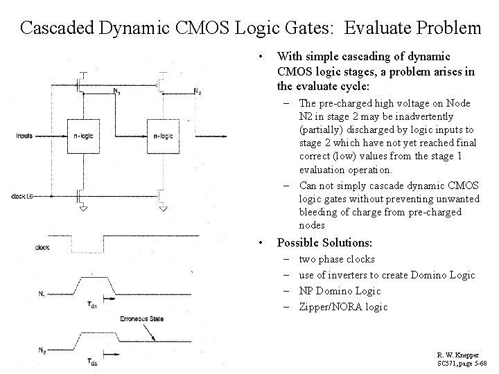
Cascaded Dynamic CMOS Logic Gates: Evaluate Problem • With simple cascading of dynamic CMOS logic stages, a problem arises in the evaluate cycle: – The pre-charged high voltage on Node N 2 in stage 2 may be inadvertently (partially) discharged by logic inputs to stage 2 which have not yet reached final correct (low) values from the stage 1 evaluation operation. – Can not simply cascade dynamic CMOS logic gates without preventing unwanted bleeding of charge from pre-charged nodes • Possible Solutions: – – two phase clocks use of inverters to create Domino Logic NP Domino Logic Zipper/NORA logic R. W. Knepper SC 571, page 5 -68

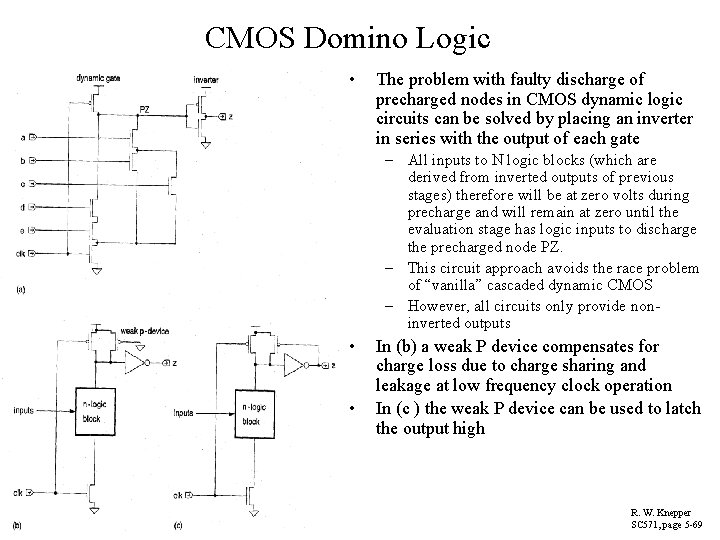
CMOS Domino Logic • The problem with faulty discharge of precharged nodes in CMOS dynamic logic circuits can be solved by placing an inverter in series with the output of each gate – All inputs to N logic blocks (which are derived from inverted outputs of previous stages) therefore will be at zero volts during precharge and will remain at zero until the evaluation stage has logic inputs to discharge the precharged node PZ. – This circuit approach avoids the race problem of “vanilla” cascaded dynamic CMOS – However, all circuits only provide noninverted outputs • • In (b) a weak P device compensates for charge loss due to charge sharing and leakage at low frequency clock operation In (c ) the weak P device can be used to latch the output high R. W. Knepper SC 571, page 5 -69

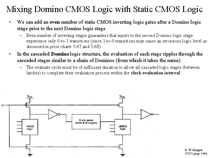
Mixing Domino CMOS Logic with Static CMOS Logic • We can add an even number of static CMOS inverting logic gates after a Domino logic stage prior to the next Domino logic stage – Even number of inverting stages guarantees that inputs to the second Domino logic stage experience only 0 -to-1 transitions (since 1 -to-0 transitions may cause an erroneous logic level as discussed in prior charts 5 -67 and 5 -68) • In the cascaded Domino logic structure, the evaluation of each stage ripples through the cascaded stages similar to a chain of Dominos (from which it takes the name) – The evaluate cycle must be of sufficient duration to allow all cascaded logic stages (between latches) to complete their evaluation process within the clock evaluation interval R. W. Knepper SC 571, page 5 -69 a

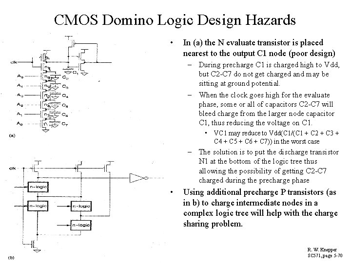
CMOS Domino Logic Design Hazards • In (a) the N evaluate transistor is placed nearest to the output C 1 node (poor design) – During precharge C 1 is charged high to Vdd, but C 2 -C 7 do not get charged and may be sitting at ground potential. – When the clock goes high for the evaluate phase, some or all of capacitors C 2 -C 7 will bleed charge from the larger node capacitor C 1, thus reducing the voltage on C 1. • VC 1 may reduce to Vdd(C 1/(C 1 + C 2 + C 3 + C 4 + C 5 + C 6 + C 7)) in the worst case – The solution is to put the discharge transistor N 1 at the bottom of the logic tree thus allowing the possibility of getting C 2 -C 7 charged during the precharge phase • Using additional precharge P transistors (as in b) to charge intermediate nodes in a complex logic tree will help with the charge sharing problem. R. W. Knepper SC 571, page 5 -70

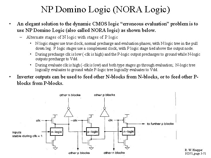
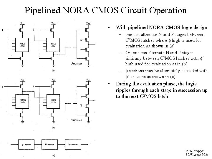
NP Domino Logic (NORA Logic) • An elegant solution to the dynamic CMOS logic “erroneous evaluation” problem is to use NP Domino Logic (also called NORA logic) as shown below. – Alternate stages of N logic with stages of P logic • N logic stages use true clock, normal precharge and evaluation phases, with N logic tree in the pull down leg. P logic stages use a complement clock, with P logic stage tied above the output node. • During precharge clk is low (-clk is high) and the P-logic output precharges to ground while N-logic outputs precharge to Vdd. • During evaluate clk is high (-clk is low) and both type stages go through evaluation; N-logic tree logically evaluates to ground while P-logic tree logically evaluates to Vdd. • Inverter outputs can be used to feed other N-blocks from N-blocks, or to feed other Pblocks from P-blocks. R. W. Knepper SC 571, page 5 -71

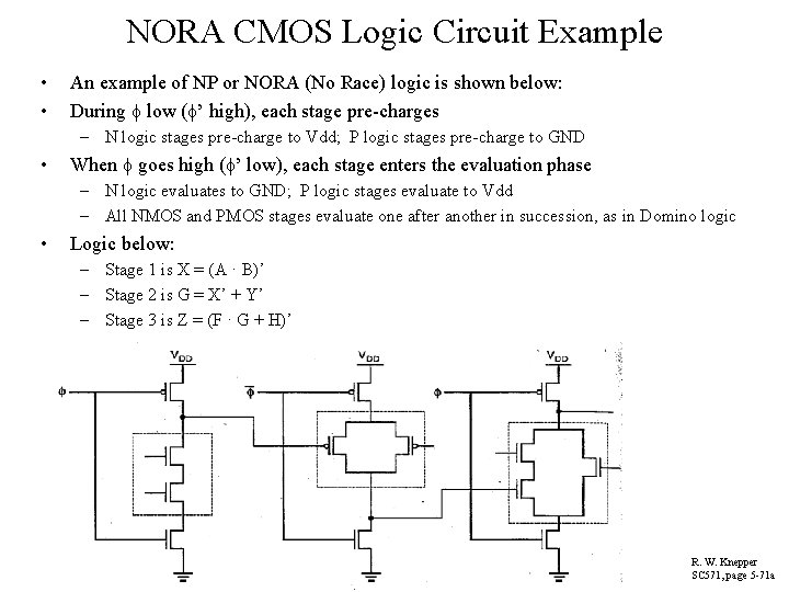
NORA CMOS Logic Circuit Example • • An example of NP or NORA (No Race) logic is shown below: During low ( ’ high), each stage pre-charges – N logic stages pre-charge to Vdd; P logic stages pre-charge to GND • When goes high ( ’ low), each stage enters the evaluation phase – N logic evaluates to GND; P logic stages evaluate to Vdd – All NMOS and PMOS stages evaluate one after another in succession, as in Domino logic • Logic below: – Stage 1 is X = (A · B)’ – Stage 2 is G = X’ + Y’ – Stage 3 is Z = (F · G + H)’ R. W. Knepper SC 571, page 5 -71 a

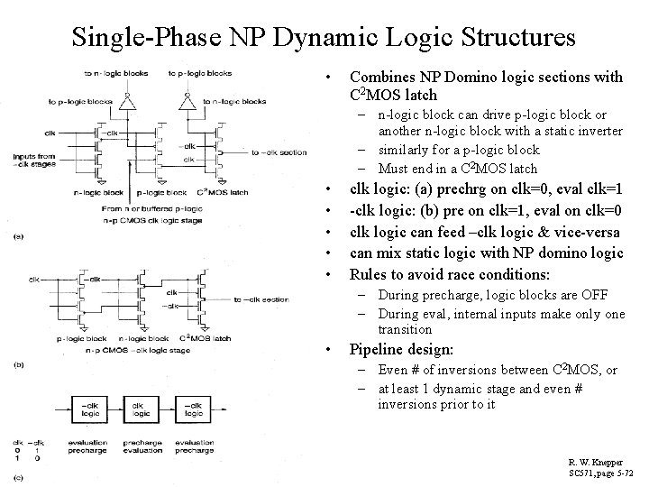
Single-Phase NP Dynamic Logic Structures • Combines NP Domino logic sections with C 2 MOS latch – n-logic block can drive p-logic block or another n-logic block with a static inverter – similarly for a p-logic block – Must end in a C 2 MOS latch • • • clk logic: (a) prechrg on clk=0, eval clk=1 -clk logic: (b) pre on clk=1, eval on clk=0 clk logic can feed –clk logic & vice-versa can mix static logic with NP domino logic Rules to avoid race conditions: – During precharge, logic blocks are OFF – During eval, internal inputs make only one transition • Pipeline design: – Even # of inversions between C 2 MOS, or – at least 1 dynamic stage and even # inversions prior to it R. W. Knepper SC 571, page 5 -72

Pipelined NORA CMOS Circuit Operation • With pipelined NORA CMOS logic design – one can alternate N and P stages between C 2 MOS latches where high is used for evaluation as shown in (a) – Or, one can alternate N and P stages similarly between C 2 MOS latches with ’ high used for evaluation as in (b) – sections may be alternately cascaded with ’ sections as shown in (c) • During the evaluation phase, the logic ripples through each stage in succession up to the next C 2 MOS latch R. W. Knepper SC 571, page 5 -72 a

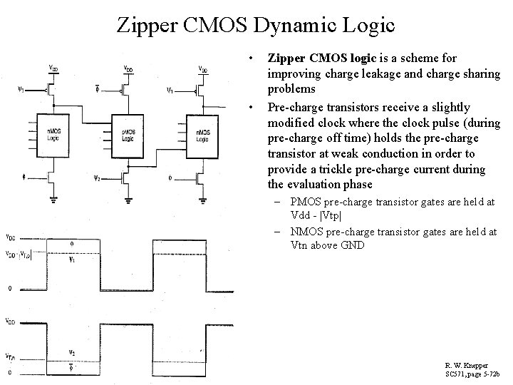
Zipper CMOS Dynamic Logic • • Zipper CMOS logic is a scheme for improving charge leakage and charge sharing problems Pre-charge transistors receive a slightly modified clock where the clock pulse (during pre-charge off time) holds the pre-charge transistor at weak conduction in order to provide a trickle pre-charge current during the evaluation phase – PMOS pre-charge transistor gates are held at Vdd - |Vtp| – NMOS pre-charge transistor gates are held at Vtn above GND R. W. Knepper SC 571, page 5 -72 b

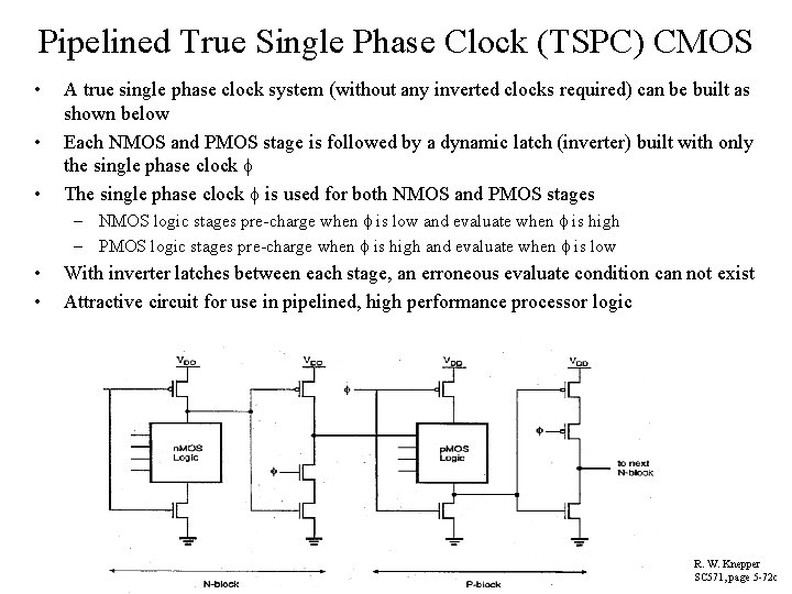
Pipelined True Single Phase Clock (TSPC) CMOS • • • A true single phase clock system (without any inverted clocks required) can be built as shown below Each NMOS and PMOS stage is followed by a dynamic latch (inverter) built with only the single phase clock The single phase clock is used for both NMOS and PMOS stages – NMOS logic stages pre-charge when is low and evaluate when is high – PMOS logic stages pre-charge when is high and evaluate when is low • • With inverter latches between each stage, an erroneous evaluate condition can not exist Attractive circuit for use in pipelined, high performance processor logic R. W. Knepper SC 571, page 5 -72 c

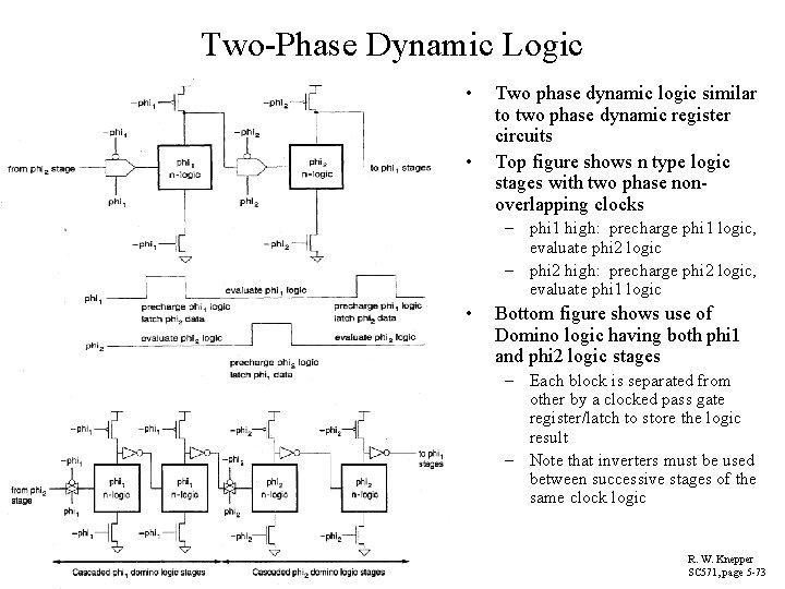
Two-Phase Dynamic Logic • • Two phase dynamic logic similar to two phase dynamic register circuits Top figure shows n type logic stages with two phase nonoverlapping clocks – phi 1 high: precharge phi 1 logic, evaluate phi 2 logic – phi 2 high: precharge phi 2 logic, evaluate phi 1 logic • Bottom figure shows use of Domino logic having both phi 1 and phi 2 logic stages – Each block is separated from other by a clocked pass gate register/latch to store the logic result – Note that inverters must be used between successive stages of the same clock logic R. W. Knepper SC 571, page 5 -73

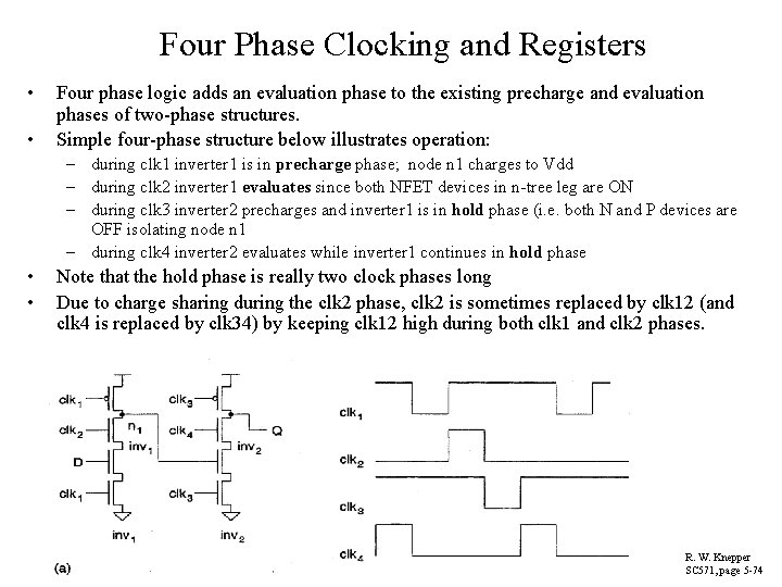
Four Phase Clocking and Registers • • Four phase logic adds an evaluation phase to the existing precharge and evaluation phases of two-phase structures. Simple four-phase structure below illustrates operation: – during clk 1 inverter 1 is in precharge phase; node n 1 charges to Vdd – during clk 2 inverter 1 evaluates since both NFET devices in n-tree leg are ON – during clk 3 inverter 2 precharges and inverter 1 is in hold phase (i. e. both N and P devices are OFF isolating node n 1 – during clk 4 inverter 2 evaluates while inverter 1 continues in hold phase • • Note that the hold phase is really two clock phases long Due to charge sharing during the clk 2 phase, clk 2 is sometimes replaced by clk 12 (and clk 4 is replaced by clk 34) by keeping clk 12 high during both clk 1 and clk 2 phases. R. W. Knepper SC 571, page 5 -74

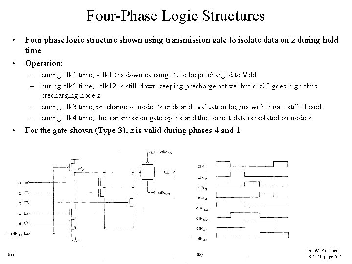
Four-Phase Logic Structures • • Four phase logic structure shown using transmission gate to isolate data on z during hold time Operation: – during clk 1 time, -clk 12 is down causing Pz to be precharged to Vdd – during clk 2 time, -clk 12 is still down keeping precharge active, but clk 23 goes high thus precharging node z – during clk 3 time, precharge of node Pz ends and evaluation begins with Xgate still closed – during clk 4 time, the transmission gate opens and the correct data is isolated on node z • For the gate shown (Type 3), z is valid during phases 4 and 1 R. W. Knepper SC 571, page 5 -75

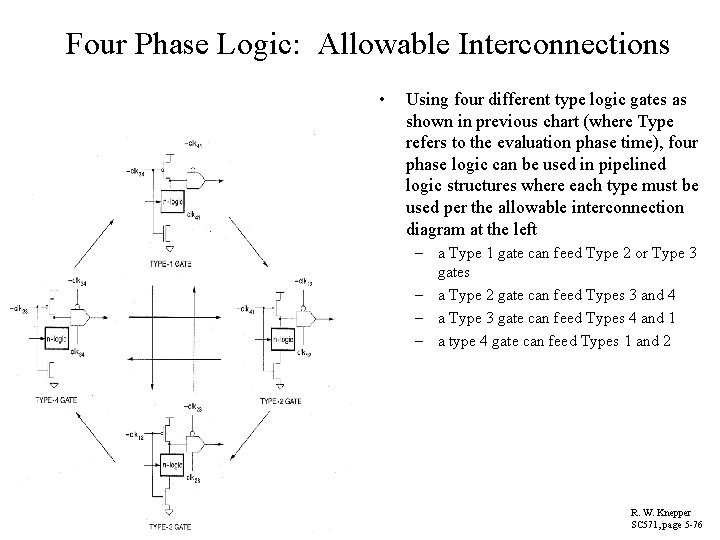
Four Phase Logic: Allowable Interconnections • Using four different type logic gates as shown in previous chart (where Type refers to the evaluation phase time), four phase logic can be used in pipelined logic structures where each type must be used per the allowable interconnection diagram at the left – a Type 1 gate can feed Type 2 or Type 3 gates – a Type 2 gate can feed Types 3 and 4 – a Type 3 gate can feed Types 4 and 1 – a type 4 gate can feed Types 1 and 2 R. W. Knepper SC 571, page 5 -76

Two-Phase Clock Generator • Phi 1 and Phi 2 clocks may be generated from a master clock using a two-phase clock generator circuit – RS type cross-coupled latch with delay built into each feedback loop – Use an even number of inverters in each feedback loop • The delay built into the feedback loop sets the non-overlap period in the two out-of-phase clocks – NOR (or NAND) gates used to synchronize the generator with a master clock input • Alternately, it may be desired to bring both phases on the chip as inputs and distribute both clocks globally R. W. Knepper SC 571, page 5 -60

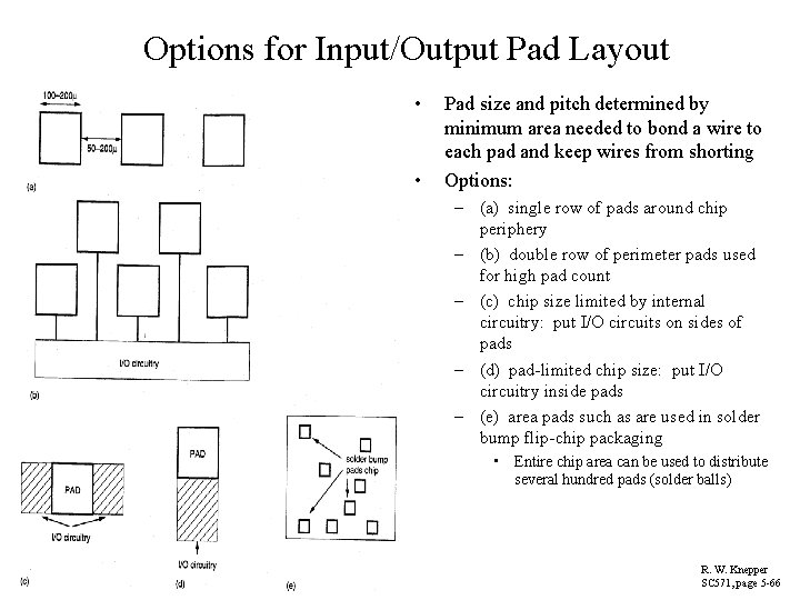
Options for Input/Output Pad Layout • • Pad size and pitch determined by minimum area needed to bond a wire to each pad and keep wires from shorting Options: – (a) single row of pads around chip periphery – (b) double row of perimeter pads used for high pad count – (c) chip size limited by internal circuitry: put I/O circuits on sides of pads – (d) pad-limited chip size: put I/O circuitry inside pads – (e) area pads such as are used in solder bump flip-chip packaging • Entire chip area can be used to distribute several hundred pads (solder balls) R. W. Knepper SC 571, page 5 -66

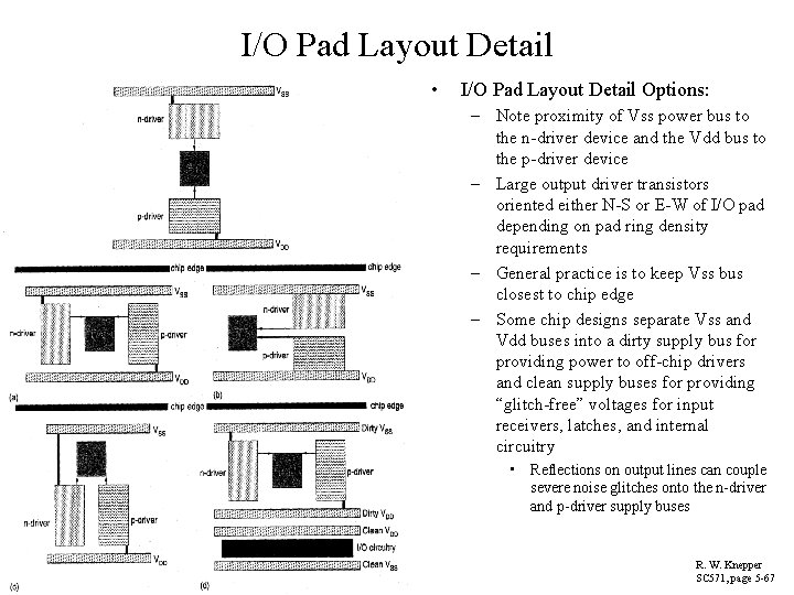
I/O Pad Layout Detail • I/O Pad Layout Detail Options: – Note proximity of Vss power bus to the n-driver device and the Vdd bus to the p-driver device – Large output driver transistors oriented either N-S or E-W of I/O pad depending on pad ring density requirements – General practice is to keep Vss bus closest to chip edge – Some chip designs separate Vss and Vdd buses into a dirty supply bus for providing power to off-chip drivers and clean supply buses for providing “glitch-free” voltages for input receivers, latches, and internal circuitry • Reflections on output lines can couple severe noise glitches onto the n-driver and p-driver supply buses R. W. Knepper SC 571, page 5 -67

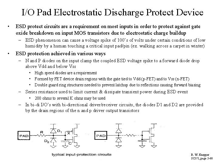
I/O Pad Electrostatic Discharge Protect Device • ESD protect circuits are a requirement on most inputs in order to protect against gate oxide breakdown on input MOS transistors due to electrostatic charge buildup – ESD phenomenon cause a voltage spike of 100’s of volts under certain conditions of low humidity by a human touching a critical input pad/pin (ex. walking across a carpet in winter) • ESD protection achieved in various ways – N and P diodes on the input clamp the coupled ESD voltage spike to a forward diode drop above Vdd and below Vss • High speed diodes are a requirement • Formed by FET device drain regions with the gate tied to Vdd (p-FET) and to Vss (n-FET) • Double guard ring structures needed to prevent latchup due to reflections causing forward biasing – Series resistance used to limit current & dissipate transient power during ESD event • 200 ohms to several K ohms may be used – In bi-di I/O’s with bi-directional driver/receiver circuits, the diodes D 1 and D 2 are provided by the drain regions of the n and p driver output transistors R. W. Knepper SC 571, page 5 -68

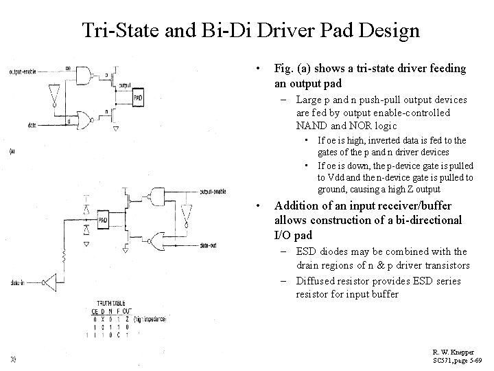
Tri-State and Bi-Di Driver Pad Design • Fig. (a) shows a tri-state driver feeding an output pad – Large p and n push-pull output devices are fed by output enable-controlled NAND and NOR logic • If oe is high, inverted data is fed to the gates of the p and n driver devices • If oe is down, the p-device gate is pulled to Vdd and the n-device gate is pulled to ground, causing a high Z output • Addition of an input receiver/buffer allows construction of a bi-directional I/O pad – ESD diodes may be combined with the drain regions of n & p driver transistors – Diffused resistor provides ESD series resistor for input buffer R. W. Knepper SC 571, page 5 -69

Bi-Directional Driver I/O Pad Symbolic Layout • Symbolic layout of a bidirectional I/O pad – Large n and p output devices formed by four parallel transistors for each • Driver drain regions double as ESD protect diodes – NAND, NOR, and inverter circuits for tri-state driver buffer are shown to the right of pad – Input buffer/inverter shown to right and above pad – Series diffused resistor shown below pad and to the right of pull-down n device – Both n and p driver devices are double guard-ringed to prevent latchup R. W. Knepper SC 571, page 5 -70

Low Voltage Swing GTL I/O Design • • Low voltage swing drivers are often needed to drive bipolar ECL inputs or to reduce dynamic power on I/O buses GTL driver (Gunning Transistor Logic) uses open-drain N pull-down output devices with 50 ohm terminating resistors connected to VT (1. 2 volts) to drive chipto-chip interconnections – Allows limited swing (0. 8 volt) chip-tochip buses to reduce ac power – Similar to bipolar open collector driver scheme used in ECL logic – Driver ckt (b) includes devices N 2 & N 3 plus INV 1 & INV 2 to reduce di/dt and limit overshoot reflections • Down level VOL is 0. 4 volt due to dc ratio with 50 ohm pull up resistor – Reduced swing input receiver (c) is a differential amplifier swinging +/- 0. 4 volt around Vref = 0. 8 volt R. W. Knepper SC 571, page 5 -71