PWE and FDTD Methods for Analysis of Photonic




- Slides: 110


PWE and FDTD Methods for Analysis of Photonic Crystals Integrated Photonics Laboratory School of Electrical Engineering Sharif University of Technology

Photonic Crystals Team n Faculty n n n Bizhan Rashidian Rahim Faez Farzad Akbari Sina Khorasani Khashayar Mehrany Students & Graduates n n n Special Acknowledgements n n n © Copyright 2005 Sharif University of Technology Alireza Dabirian Amir Hossein Atabaki Amir Hosseini Meysamreza Chamanzar Mohammad Ali Mahmoodzadeh Keyhan Kobravi Sadjad Jahanbakht Maryam Safari 1 st Workshop on Photonic Crystals Mashad, Iran, September 2005

Outline n Plane Wave Expansion (PWE) n E- and H-Polarizations n Sharif PWE Code n Typical n Band Structures Finite Difference Time Domain (FDTD) n Description of Method n Boundary Conditions Bloch Boundary Condition n Perfectly Matched Layer n Symmetric Boundary Condition n © Copyright 2005 Sharif University of Technology 1 st Workshop on Photonic Crystals Mashad, Iran, September 2005

Outline FDTD Sources n Sharif FDTD Analysis Interface & Tool n n Band Structure n Comparison to PWE/FEM n Defective Structures n n n Waveguide Cavity Coupled-Resonator Optical Waveguide Photonic Crystal Slab Waveguide Conclusions © Copyright 2005 Sharif University of Technology 1 st Workshop on Photonic Crystals Mashad, Iran, September 2005

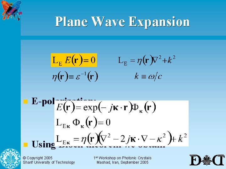
Plane Wave Expansion n E-polarization: n Using Bloch theorem we obtain © Copyright 2005 Sharif University of Technology 1 st Workshop on Photonic Crystals Mashad, Iran, September 2005

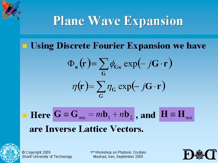
Plane Wave Expansion n Using Discrete Fourier Expansion we have n Here , and are Inverse Lattice Vectors. © Copyright 2005 Sharif University of Technology 1 st Workshop on Photonic Crystals Mashad, Iran, September 2005

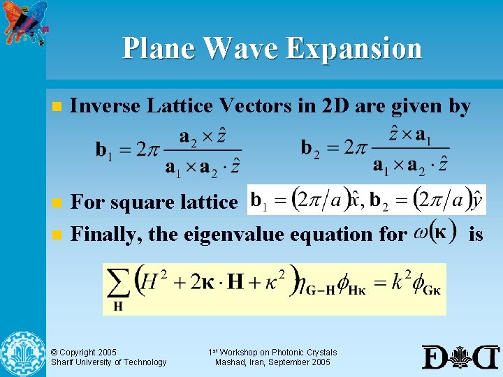
Plane Wave Expansion n Inverse Lattice Vectors in 2 D are given by n For square lattice Finally, the eigenvalue equation for n © Copyright 2005 Sharif University of Technology 1 st Workshop on Photonic Crystals Mashad, Iran, September 2005 is

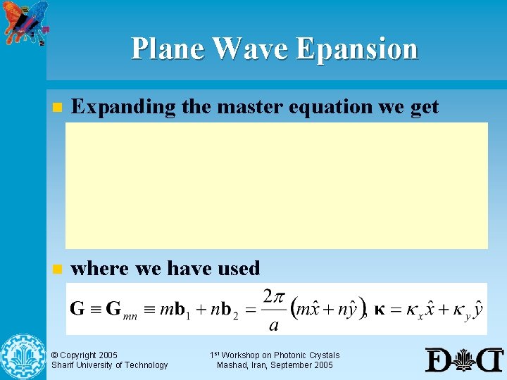
Plane Wave Epansion n Expanding the master equation we get n where we have used © Copyright 2005 Sharif University of Technology 1 st Workshop on Photonic Crystals Mashad, Iran, September 2005

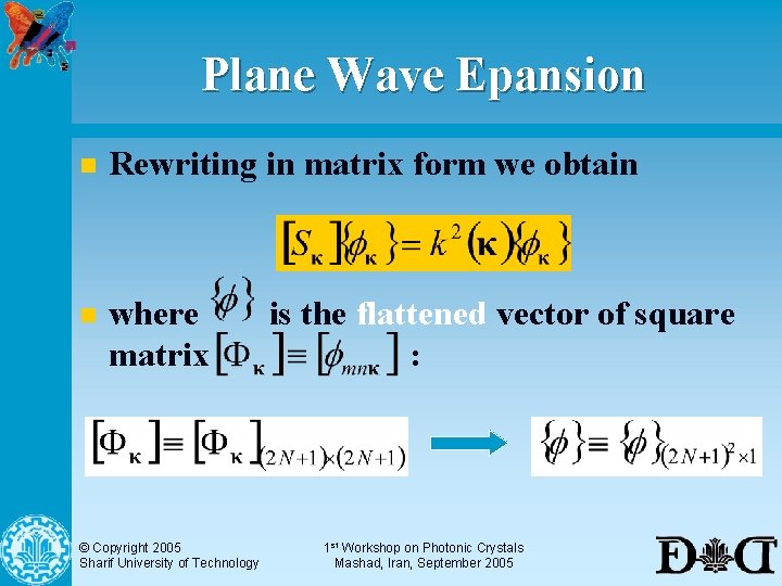
Plane Wave Epansion n Rewriting in matrix form we obtain n where matrix © Copyright 2005 Sharif University of Technology is the flattened vector of square : 1 st Workshop on Photonic Crystals Mashad, Iran, September 2005

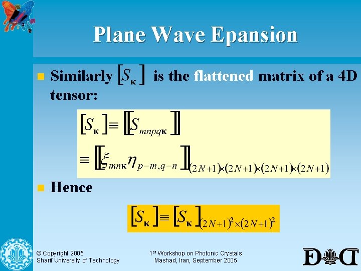
Plane Wave Epansion n Similarly tensor: n Hence © Copyright 2005 Sharif University of Technology is the flattened matrix of a 4 D 1 st Workshop on Photonic Crystals Mashad, Iran, September 2005

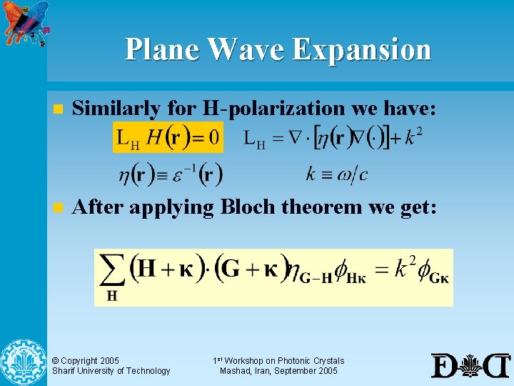
Plane Wave Expansion n Similarly for H-polarization we have: n After applying Bloch theorem we get: © Copyright 2005 Sharif University of Technology 1 st Workshop on Photonic Crystals Mashad, Iran, September 2005

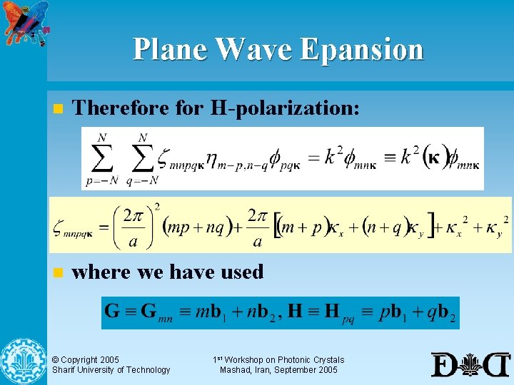
Plane Wave Epansion n Therefore for H-polarization: n where we have used © Copyright 2005 Sharif University of Technology 1 st Workshop on Photonic Crystals Mashad, Iran, September 2005

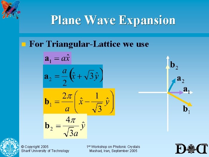
Plane Wave Expansion n For Triangular-Lattice we use © Copyright 2005 Sharif University of Technology 1 st Workshop on Photonic Crystals Mashad, Iran, September 2005

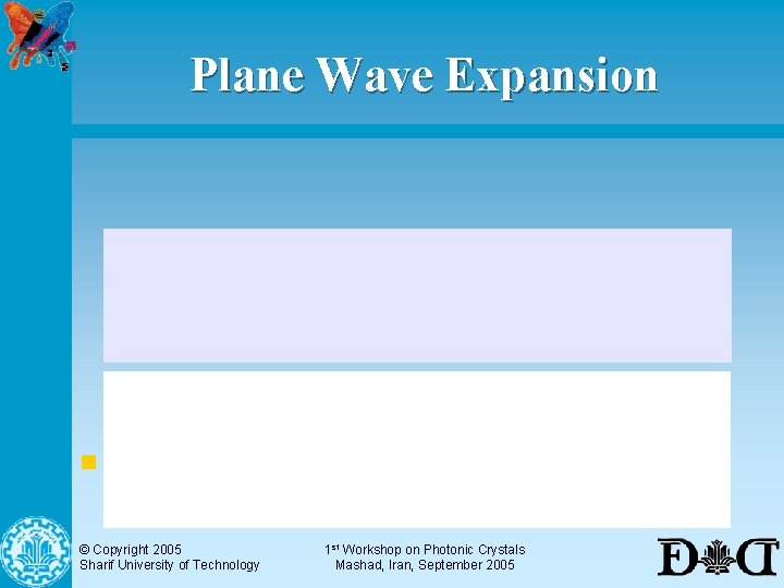
Plane Wave Expansion n Hence for E- and H-polarizations in triangular lattice we respectively get © Copyright 2005 Sharif University of Technology 1 st Workshop on Photonic Crystals Mashad, Iran, September 2005

Sharif PWE Code n n Written in MATLAB Input arguments: N: Number of Plane Waves n R: Number of Divisions on Each Side of BZ n a: Lattice Constant (default value is 1) n r: Radius of Holes/Rods n e 1: Permittivity of Holes/Rods n e 2: Permittivity of Host Medium n © Copyright 2005 Sharif University of Technology 1 st Workshop on Photonic Crystals Mashad, Iran, September 2005

Typical Band Structures n Infinitesimal perturbations in vacuum © Copyright 2005 Sharif University of Technology 1 st Workshop on Photonic Crystals Mashad, Iran, September 2005

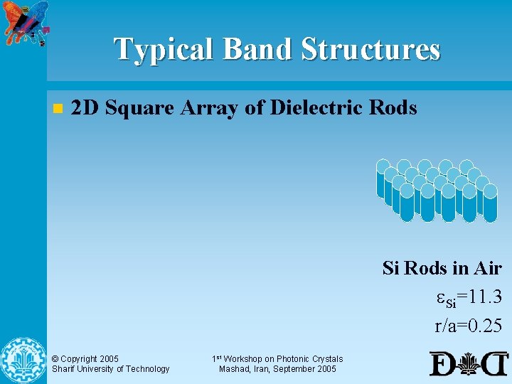
Typical Band Structures n 2 D Square Array of Dielectric Rods Si Rods in Air e. Si=11. 3 r/a=0. 25 © Copyright 2005 Sharif University of Technology 1 st Workshop on Photonic Crystals Mashad, Iran, September 2005

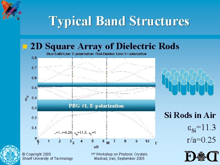
Typical Band Structures n 2 D Square Array of Dielectric Rods PBG #1, E-polarization Si Rods in Air e. Si=11. 3 r/a=0. 25 © Copyright 2005 Sharif University of Technology 1 st Workshop on Photonic Crystals Mashad, Iran, September 2005

Typical Band Structures n Band Surface #1 © Copyright 2005 Sharif University of Technology 1 st Workshop on Photonic Crystals Mashad, Iran, September 2005

Typical Band Structures n Band Surface #2 © Copyright 2005 Sharif University of Technology 1 st Workshop on Photonic Crystals Mashad, Iran, September 2005

Typical Band Structures n Band Surface #3 © Copyright 2005 Sharif University of Technology 1 st Workshop on Photonic Crystals Mashad, Iran, September 2005

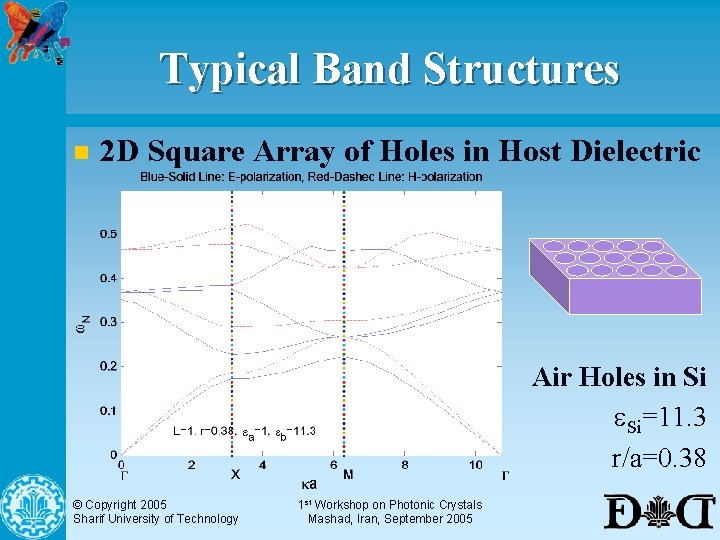
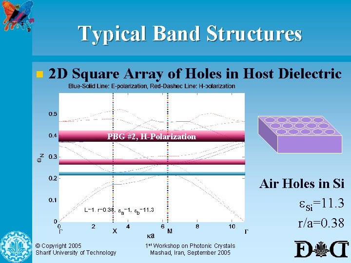
Typical Band Structures n 2 D Square Array of Holes in Host Dielectric Air Holes in Si e. Si=11. 3 r/a=0. 38 © Copyright 2005 Sharif University of Technology 1 st Workshop on Photonic Crystals Mashad, Iran, September 2005

Typical Band Structures n 2 D Square Array of Holes in Host Dielectric PBG #2, H-Polarization Air Holes in Si e. Si=11. 3 r/a=0. 38 © Copyright 2005 Sharif University of Technology 1 st Workshop on Photonic Crystals Mashad, Iran, September 2005

Typical Band Structures n Band Surface #1 © Copyright 2005 Sharif University of Technology 1 st Workshop on Photonic Crystals Mashad, Iran, September 2005

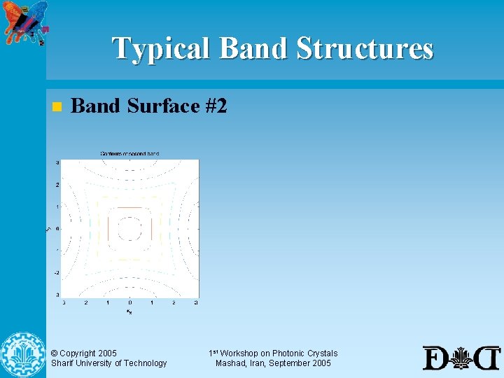
Typical Band Structures n Band Surface #2 © Copyright 2005 Sharif University of Technology 1 st Workshop on Photonic Crystals Mashad, Iran, September 2005

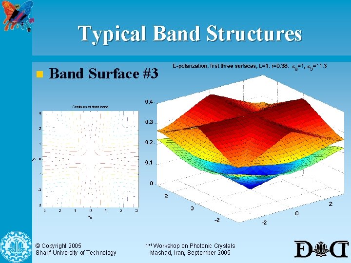
Typical Band Structures n Band Surface #3 © Copyright 2005 Sharif University of Technology 1 st Workshop on Photonic Crystals Mashad, Iran, September 2005

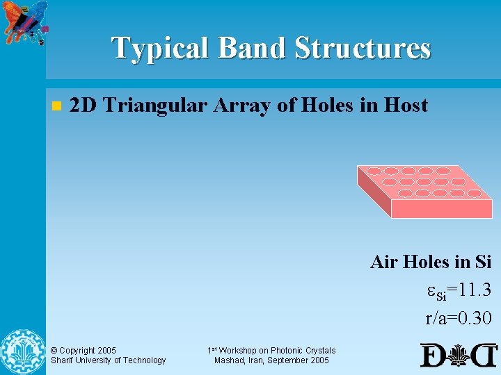
Typical Band Structures n 2 D Triangular Array of Holes in Host Air Holes in Si e. Si=11. 3 r/a=0. 30 © Copyright 2005 Sharif University of Technology 1 st Workshop on Photonic Crystals Mashad, Iran, September 2005

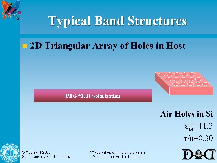
Typical Band Structures n 2 D Triangular Array of Holes in Host PBG #1, H-polarization Air Holes in Si e. Si=11. 3 r/a=0. 30 © Copyright 2005 Sharif University of Technology 1 st Workshop on Photonic Crystals Mashad, Iran, September 2005

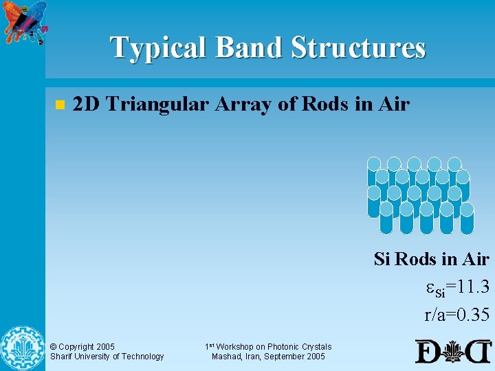
Typical Band Structures n 2 D Triangular Array of Rods in Air Si Rods in Air e. Si=11. 3 r/a=0. 35 © Copyright 2005 Sharif University of Technology 1 st Workshop on Photonic Crystals Mashad, Iran, September 2005

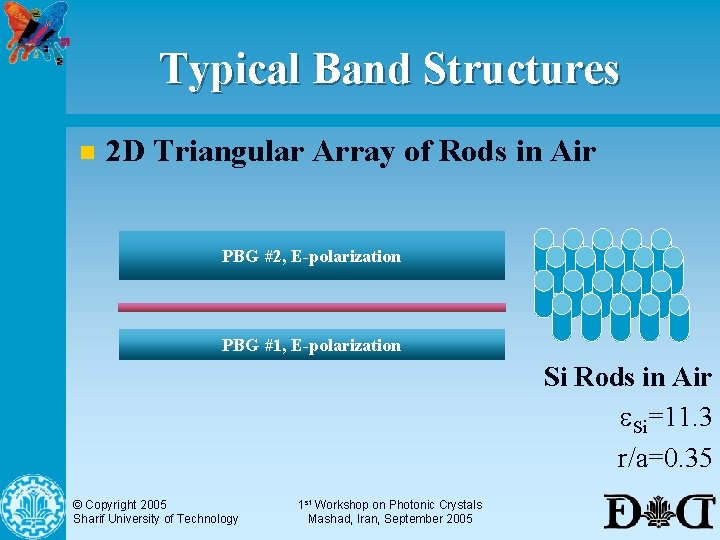
Typical Band Structures n 2 D Triangular Array of Rods in Air PBG #2, E-polarization PBG #1, E-polarization Si Rods in Air e. Si=11. 3 r/a=0. 35 © Copyright 2005 Sharif University of Technology 1 st Workshop on Photonic Crystals Mashad, Iran, September 2005

Why FDTD ? n n n Once run, information of the system in the whole frequency spectrum is achieved Capable of modal analysis with Fourier transforming No matrix inversion is needed, thanks to the explicit scheme n n This is extremely advantageous in large configurations with many components Very efficient for parallel processing © Copyright 2005 Sharif University of Technology 1 st Workshop on Photonic Crystals Mashad, Iran, September 2005

Description of 3 D FDTD n n n Yee proposed a scheme in 1966 for time domain calculation of Maxwell’s equations FDTD was not practical until the advent of faster processors and larger memories in mid 1970 s Taflove coined the acronym FDTD in 1970 s © Copyright 2005 Sharif University of Technology 1 st Workshop on Photonic Crystals Mashad, Iran, September 2005

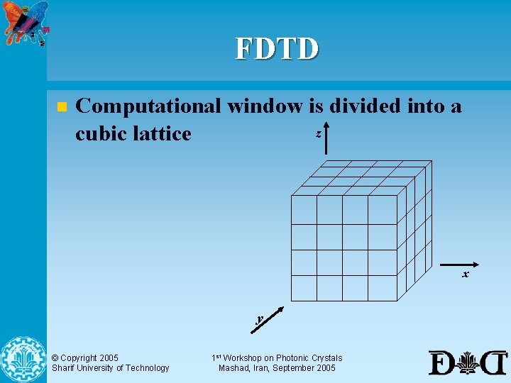
FDTD n Computational window is divided into a z cubic lattice x y © Copyright 2005 Sharif University of Technology 1 st Workshop on Photonic Crystals Mashad, Iran, September 2005

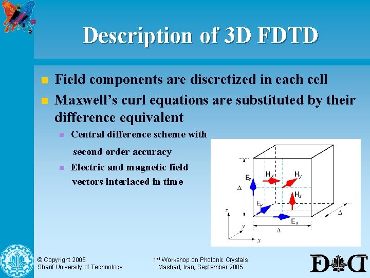
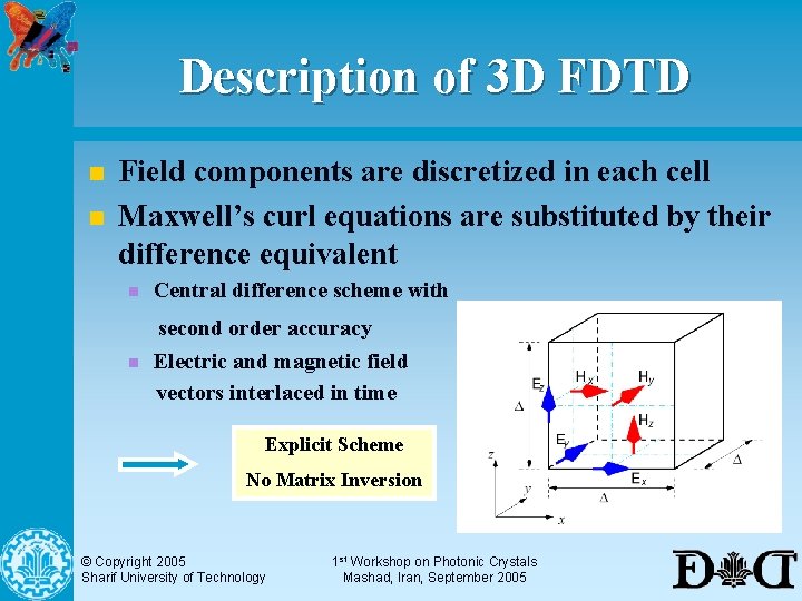
Description of 3 D FDTD n n Field components are discretized in each cell Maxwell’s curl equations are substituted by their difference equivalent n Central difference scheme with n second order accuracy Electric and magnetic field vectors interlaced in time © Copyright 2005 Sharif University of Technology 1 st Workshop on Photonic Crystals Mashad, Iran, September 2005

Description of 3 D FDTD n n Field components are discretized in each cell Maxwell’s curl equations are substituted by their difference equivalent n Central difference scheme with n second order accuracy Electric and magnetic field vectors interlaced in time Explicit Scheme No Matrix Inversion © Copyright 2005 Sharif University of Technology 1 st Workshop on Photonic Crystals Mashad, Iran, September 2005

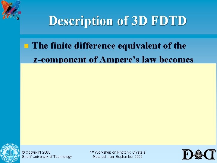
Description of 3 D FDTD n The finite difference equivalent of the z-component of Ampere’s law becomes © Copyright 2005 Sharif University of Technology 1 st Workshop on Photonic Crystals Mashad, Iran, September 2005

Features of FDTD n n Maxwell’s integral equations are satisfied as the same time. Maxwell’s equations, rather than Helmholtz equation is solved n n Both electric and magnetic field boundary conditions are met explicitly Maxwell’s divergence equations are simultaneously satisfied, because of the location of the field components Interlacing of the electric and magnetic fields in time, makes the scheme explicit No matrix inversion is needed © Copyright 2005 Sharif University of Technology 1 st Workshop on Photonic Crystals Mashad, Iran, September 2005

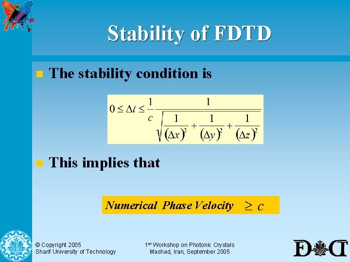
Stability of FDTD n The stability condition is n This implies that Numerical Phase Velocity © Copyright 2005 Sharif University of Technology 1 st Workshop on Photonic Crystals Mashad, Iran, September 2005

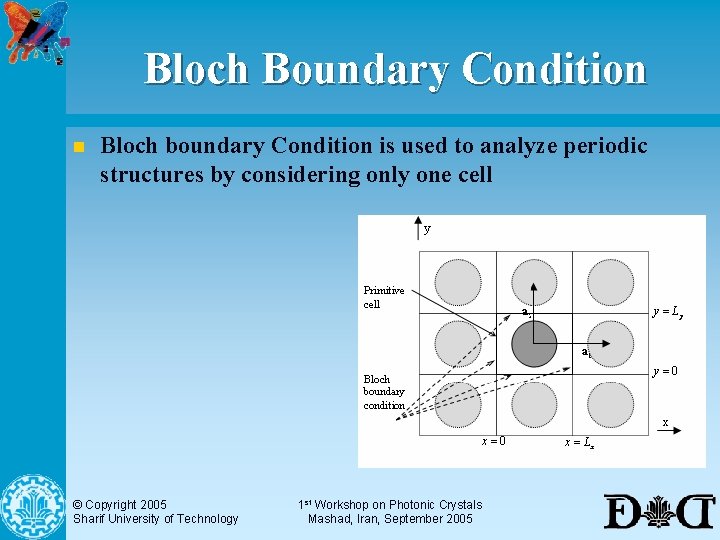
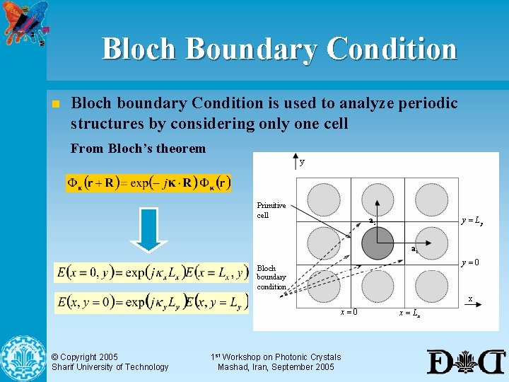
Bloch Boundary Condition n Bloch boundary Condition is used to analyze periodic structures by considering only one cell © Copyright 2005 Sharif University of Technology 1 st Workshop on Photonic Crystals Mashad, Iran, September 2005

Bloch Boundary Condition n Bloch boundary Condition is used to analyze periodic structures by considering only one cell From Bloch’s theorem © Copyright 2005 Sharif University of Technology 1 st Workshop on Photonic Crystals Mashad, Iran, September 2005

Symmetry Boundary Condition n If the structure is symmetric with respect to a plane, the electromagnetic field components are either even or odd with respect to the same plane. The computational efficiency is greatly enhanced Degenerate modes can be studied separately © Copyright 2005 Sharif University of Technology 1 st Workshop on Photonic Crystals Mashad, Iran, September 2005

Perfectly Matched Layer n For transparent boundaries we need a boundary condition which should n Has zero reflection to incoming waves n Any frequency n Any polarization n Any angle of incidence Be thin n Effective near sources n © Copyright 2005 Sharif University of Technology 1 st Workshop on Photonic Crystals Mashad, Iran, September 2005

Perfectly Matched Layer n In 1994 Bereneger constructed a boundary layer that perfectly matched to all incoming waves. It dissipates the wave within itself. n It terminates to other symmetry boundary conditions, itself. n It is based on a field-splitting technique, so that in 3 D we get 12 equations rather than 6, therefore there is no physical insight. n © Copyright 2005 Sharif University of Technology 1 st Workshop on Photonic Crystals Mashad, Iran, September 2005

Perfectly Matched Layer n n n Gedney proposed another model for PML in 1996 that outperformed the Bereneger’s original model. Gendney’s PML is modeled by a lossy anisotropic media, directly explained by nonmodified Maxwell’s equations. Reflection from PML is typically -120 d. B, but it can be as low as -200 d. B. © Copyright 2005 Sharif University of Technology 1 st Workshop on Photonic Crystals Mashad, Iran, September 2005

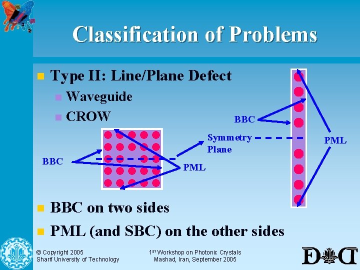
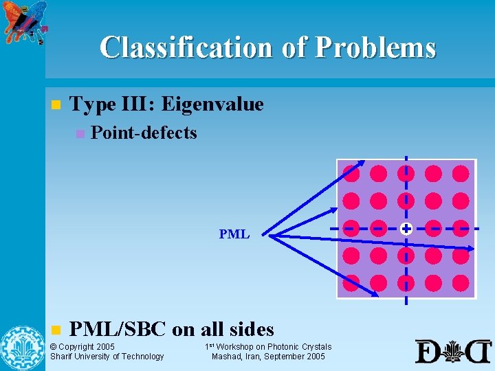
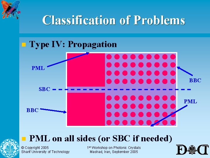
Classification of Problems n Photonic crystal problems with regard to the boundary conditions can be generally categorized into three groups Type I: Crystal Band-Structure n Type II: Line/Plane Defect Band-Structure n Type III: Eigenvalue n Type IV: Propagation n © Copyright 2005 Sharif University of Technology 1 st Workshop on Photonic Crystals Mashad, Iran, September 2005

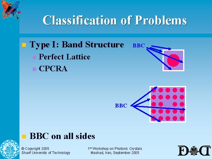
Classification of Problems n Type I: Band Structure BBC Perfect Lattice n CPCRA n BBC on all sides © Copyright 2005 Sharif University of Technology 1 st Workshop on Photonic Crystals Mashad, Iran, September 2005

Classification of Problems n Type II: Line/Plane Defect Waveguide n CROW n BBC Symmetry Plane BBC n n PML BBC on two sides PML (and SBC) on the other sides © Copyright 2005 Sharif University of Technology 1 st Workshop on Photonic Crystals Mashad, Iran, September 2005 PML

Classification of Problems n Type III: Eigenvalue n Point-defects PML n PML/SBC on all sides © Copyright 2005 Sharif University of Technology 1 st Workshop on Photonic Crystals Mashad, Iran, September 2005

Classification of Problems n Type IV: Propagation PML BBC SBC PML BBC n PML on all sides (or SBC if needed) © Copyright 2005 Sharif University of Technology 1 st Workshop on Photonic Crystals Mashad, Iran, September 2005

FDTD Sources n Type I/II/III: n n Initial Field Type IV: n Point Source n Sinusoidal/Gaussian n in Time Huygens’ Source (radiates only in one direction) n Sinusoidal/Gaussian in Time n Gaussian in Space n Slab Waveguide Eigenmode © Copyright 2005 Sharif University of Technology 1 st Workshop on Photonic Crystals Mashad, Iran, September 2005

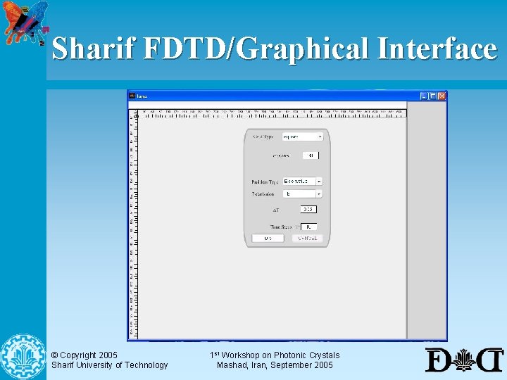
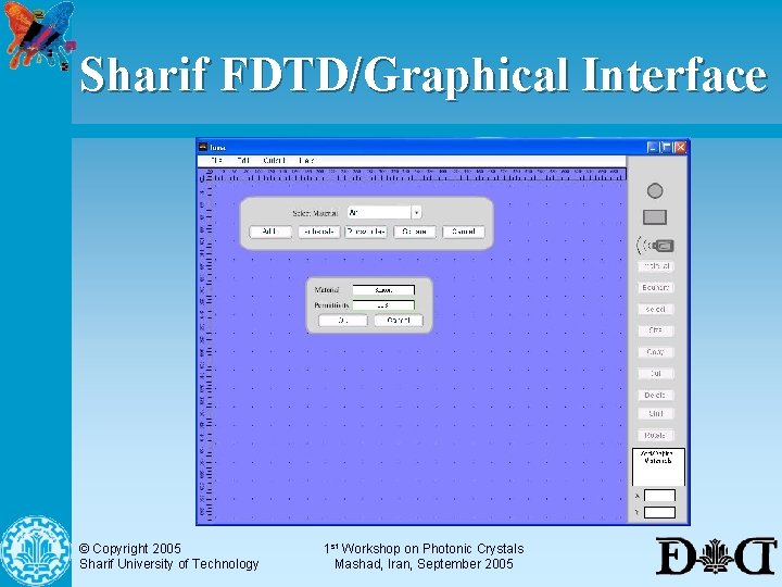
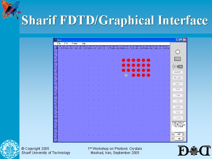
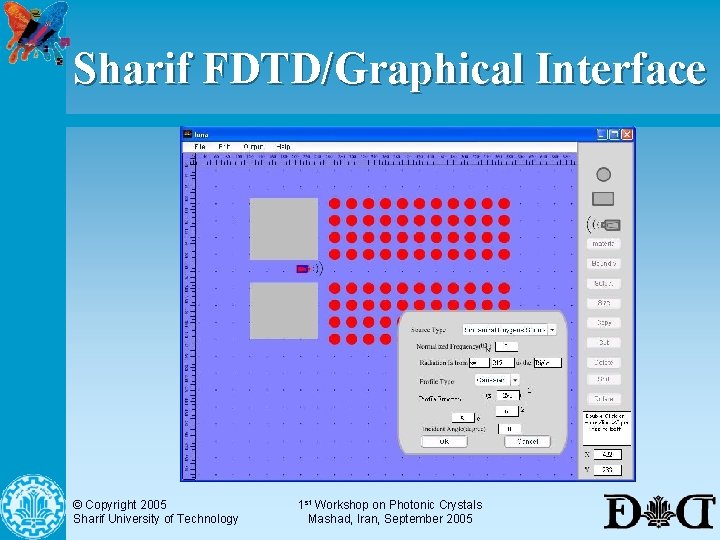
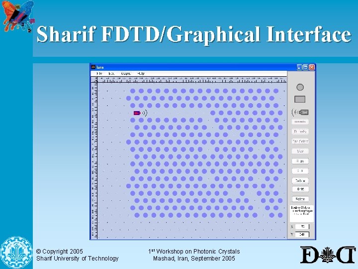
Sharif FDTD n Sharif FDTD Code Written in C++ n 2 D/3 D n Supports Initial Field, Point Source, Huygens’ Source n n n Visual Basic Graphical Interface for 2 D structures and slab waveguides (3 D under development) MATLAB Graphics Post-processor © Copyright 2005 Sharif University of Technology 1 st Workshop on Photonic Crystals Mashad, Iran, September 2005

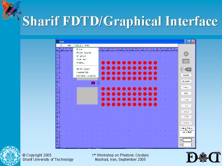
Sharif FDTD n Outputs Band-Structure n Waveguide Band-Structure n Probe n Field Snapshots (Animations) n Power-plane Integrator n © Copyright 2005 Sharif University of Technology 1 st Workshop on Photonic Crystals Mashad, Iran, September 2005

Sharif FDTD/Graphical Interface © Copyright 2005 Sharif University of Technology 1 st Workshop on Photonic Crystals Mashad, Iran, September 2005

Sharif FDTD/Graphical Interface © Copyright 2005 Sharif University of Technology 1 st Workshop on Photonic Crystals Mashad, Iran, September 2005

Sharif FDTD/Graphical Interface © Copyright 2005 Sharif University of Technology 1 st Workshop on Photonic Crystals Mashad, Iran, September 2005

Sharif FDTD/Graphical Interface © Copyright 2005 Sharif University of Technology 1 st Workshop on Photonic Crystals Mashad, Iran, September 2005

Sharif FDTD/Graphical Interface © Copyright 2005 Sharif University of Technology 1 st Workshop on Photonic Crystals Mashad, Iran, September 2005

Sharif FDTD/Graphical Interface © Copyright 2005 Sharif University of Technology 1 st Workshop on Photonic Crystals Mashad, Iran, September 2005

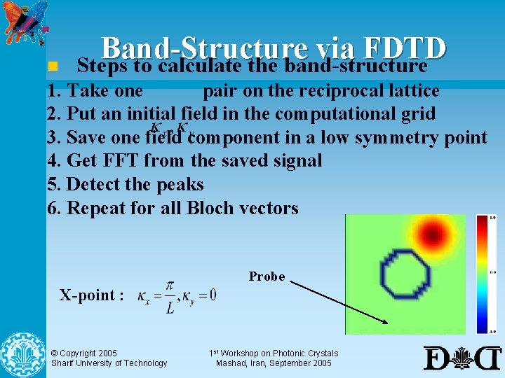
n Band-Structure via FDTD Steps to calculate the band-structure 1. Take one pair on the reciprocal lattice 2. Put an initial field in the computational grid 3. Save one field component in a low symmetry point 4. Get FFT from the saved signal 5. Detect the peaks 6. Repeat for all Bloch vectors Probe X-point : © Copyright 2005 Sharif University of Technology 1 st Workshop on Photonic Crystals Mashad, Iran, September 2005

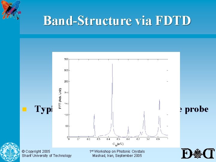
Band-Structure via FDTD n Typical spectrum obtained from the probe © Copyright 2005 Sharif University of Technology 1 st Workshop on Photonic Crystals Mashad, Iran, September 2005

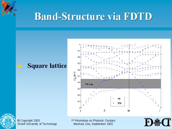
Band-Structure via FDTD n Square lattice of dielectric rods © Copyright 2005 Sharif University of Technology 1 st Workshop on Photonic Crystals Mashad, Iran, September 2005

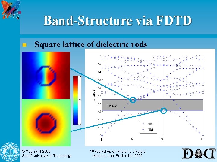
Band-Structure via FDTD n Square lattice of dielectric rods © Copyright 2005 Sharif University of Technology 1 st Workshop on Photonic Crystals Mashad, Iran, September 2005

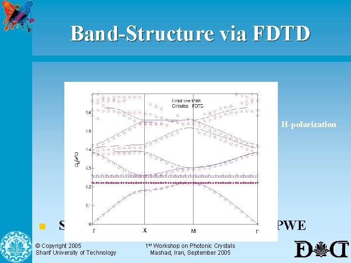
Band-Structure via FDTD H-polarization n Square lattice of air holes; FDTD vs. PWE © Copyright 2005 Sharif University of Technology 1 st Workshop on Photonic Crystals Mashad, Iran, September 2005

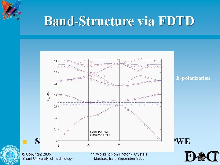
Band-Structure via FDTD E-polarization n Square lattice of air holes; FDTD vs. PWE © Copyright 2005 Sharif University of Technology 1 st Workshop on Photonic Crystals Mashad, Iran, September 2005

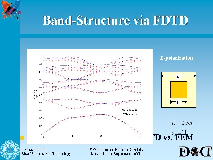
Band-Structure via FDTD E-polarization a L n Square lattice of square rods; FDTD vs. FEM © Copyright 2005 Sharif University of Technology 1 st Workshop on Photonic Crystals Mashad, Iran, September 2005

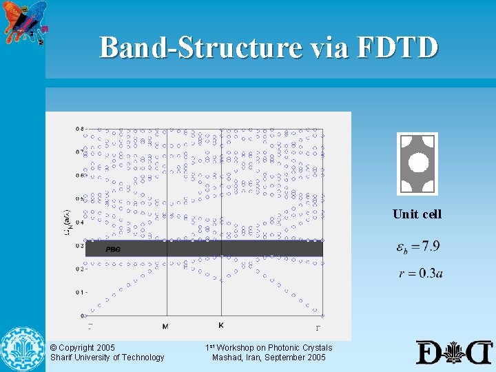
Band-Structure via FDTD Unit cell n Triangular lattice of air holes © Copyright 2005 Sharif University of Technology 1 st Workshop on Photonic Crystals Mashad, Iran, September 2005

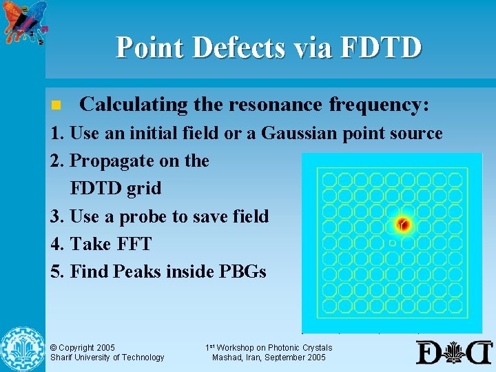
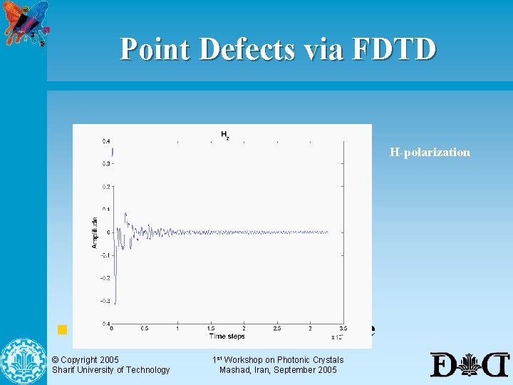
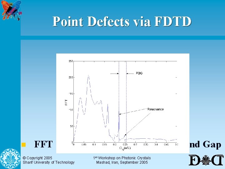
Point Defects via FDTD n Calculating the resonance frequency: 1. Use an initial field or a Gaussian point source 2. Propagate on the FDTD grid 3. Use a probe to save field 4. Take FFT 5. Find Peaks inside PBGs © Copyright 2005 Sharif University of Technology 1 st Workshop on Photonic Crystals Mashad, Iran, September 2005

Point Defects via FDTD H-polarization n Time-domain output of probe © Copyright 2005 Sharif University of Technology 1 st Workshop on Photonic Crystals Mashad, Iran, September 2005

Point Defects via FDTD n FFT Spectrum near the Photonic Band Gap © Copyright 2005 Sharif University of Technology 1 st Workshop on Photonic Crystals Mashad, Iran, September 2005

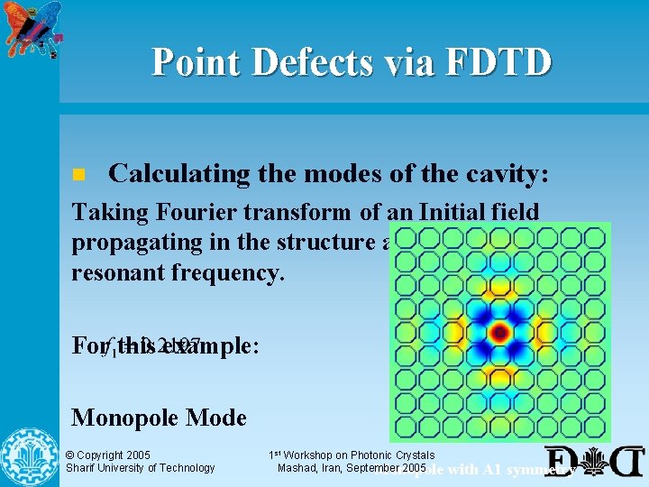
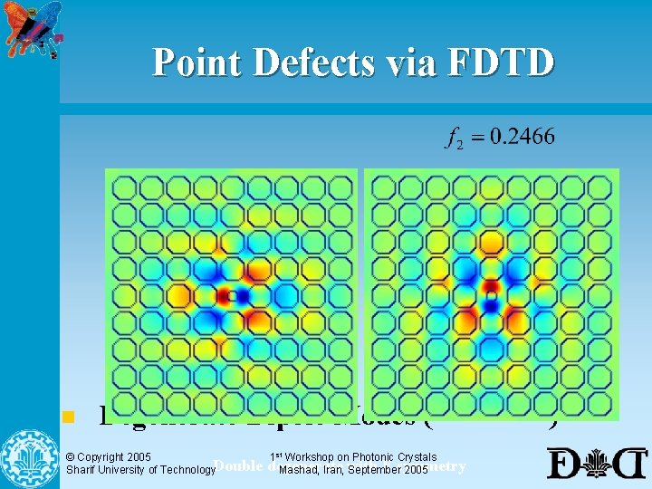
Point Defects via FDTD n Calculating the modes of the cavity: Taking Fourier transform of an Initial field propagating in the structure at each grid, at the resonant frequency. For this example: Monopole Mode © Copyright 2005 Sharif University of Technology 1 st Workshop on Photonic Crystals Mashad, Iran, September 2005 Monopole with A 1 symmetry

Point Defects via FDTD n Degenerate Dipole Modes ( 1 st Workshop on Photonic Crystals © Copyright 2005 E symmetry Mashad, Iran, with September 2005 Sharif University of Technology. Double degenerate )

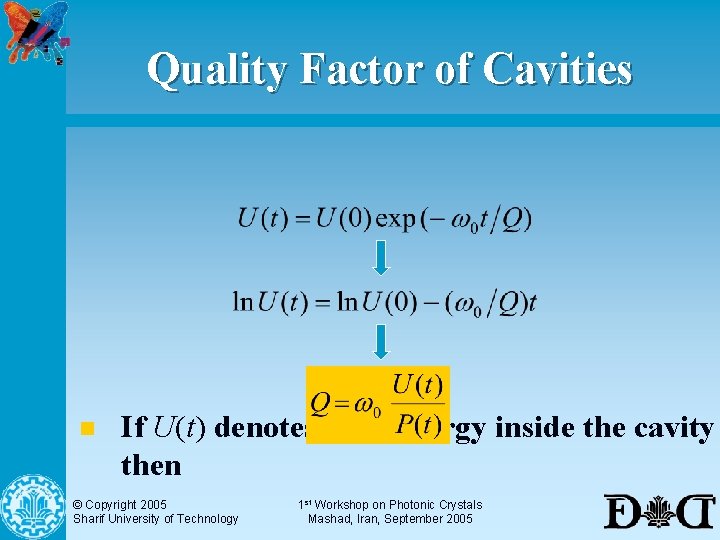
Quality Factor of Cavities n If U(t) denotes total energy inside the cavity then © Copyright 2005 Sharif University of Technology 1 st Workshop on Photonic Crystals Mashad, Iran, September 2005

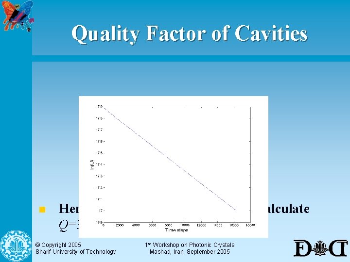
Quality Factor of Cavities n Hence for the Monopole Mode we calculate Q=315 from the slope of energy loss. © Copyright 2005 Sharif University of Technology 1 st Workshop on Photonic Crystals Mashad, Iran, September 2005

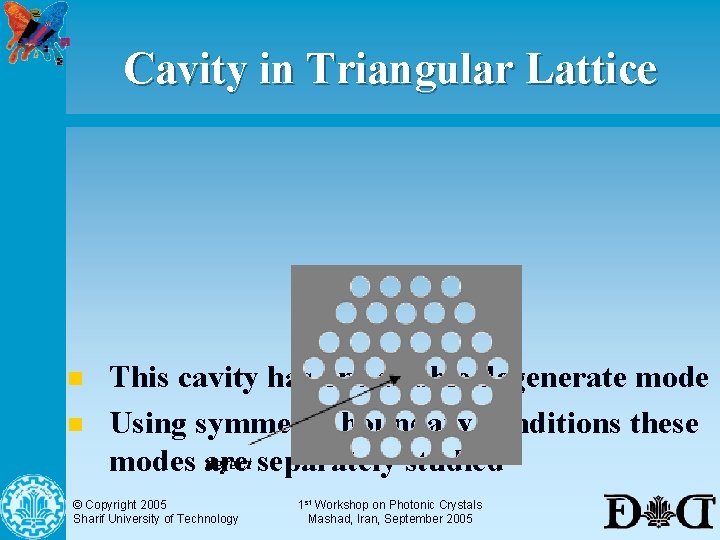
Cavity in Triangular Lattice n n This cavity has one double degenerate mode Using symmetry boundary conditions these modes are separately studied © Copyright 2005 Sharif University of Technology 1 st Workshop on Photonic Crystals Mashad, Iran, September 2005

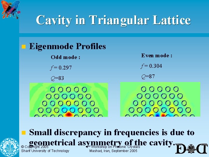
Cavity in Triangular Lattice n n Eigenmode Profiles Odd mode : Even mode : f = 0. 297 f = 0. 304 Q=83 Q=87 Small discrepancy in frequencies is due to geometrical asymmetry of the cavity. © Copyright 2005 Sharif University of Technology 1 st Workshop on Photonic Crystals Mashad, Iran, September 2005

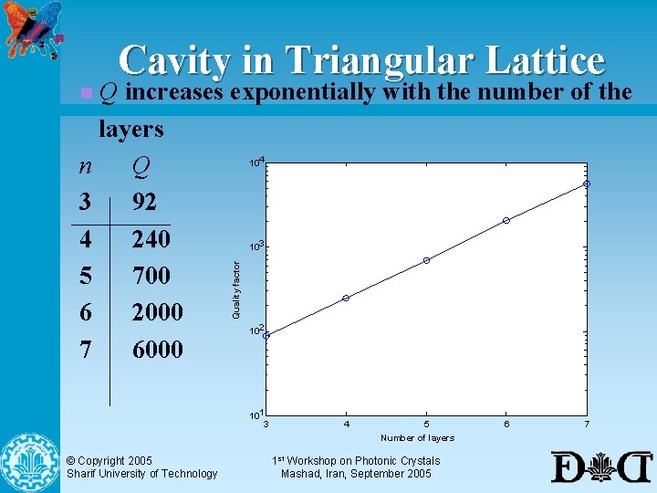
Cavity in Triangular Lattice Q increases exponentially with the number of the layers n Q 3 92 4 240 5 700 6 2000 7 6000 n 104 Quality factor 103 102 101 3 4 5 Number of layers © Copyright 2005 Sharif University of Technology 1 st Workshop on Photonic Crystals Mashad, Iran, September 2005 6 7

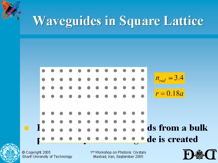
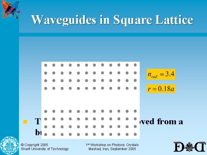
Waveguides in Square Lattice n By removing one row of rods from a bulk photonic crystal a waveguide is created © Copyright 2005 Sharif University of Technology 1 st Workshop on Photonic Crystals Mashad, Iran, September 2005

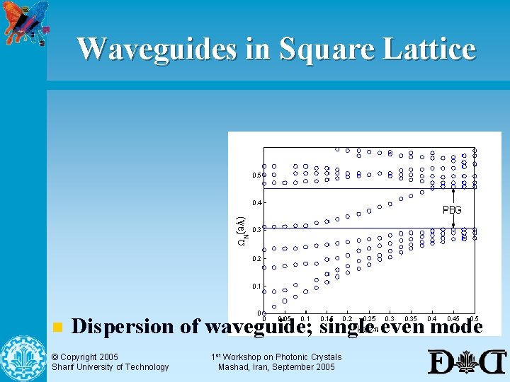
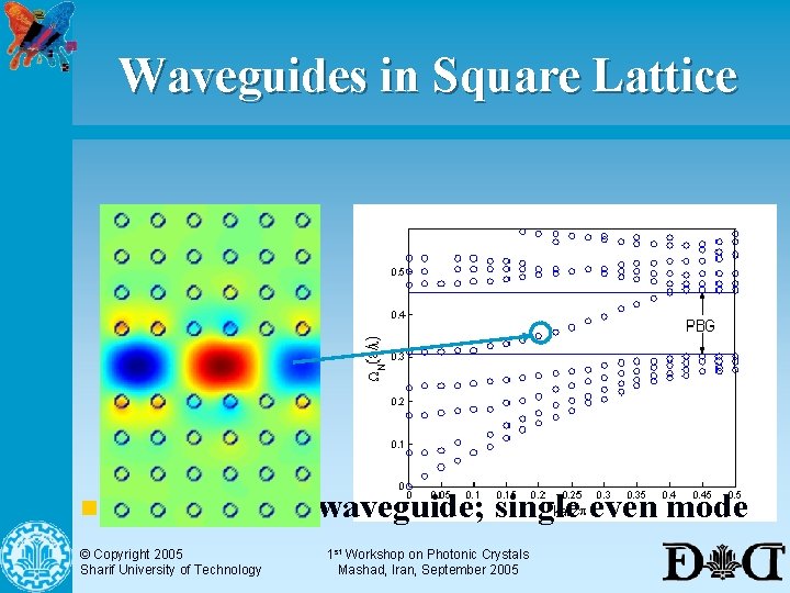
Waveguides in Square Lattice n Dispersion of waveguide; single even mode © Copyright 2005 Sharif University of Technology 1 st Workshop on Photonic Crystals Mashad, Iran, September 2005

Waveguides in Square Lattice n Dispersion of waveguide; single even mode © Copyright 2005 Sharif University of Technology 1 st Workshop on Photonic Crystals Mashad, Iran, September 2005

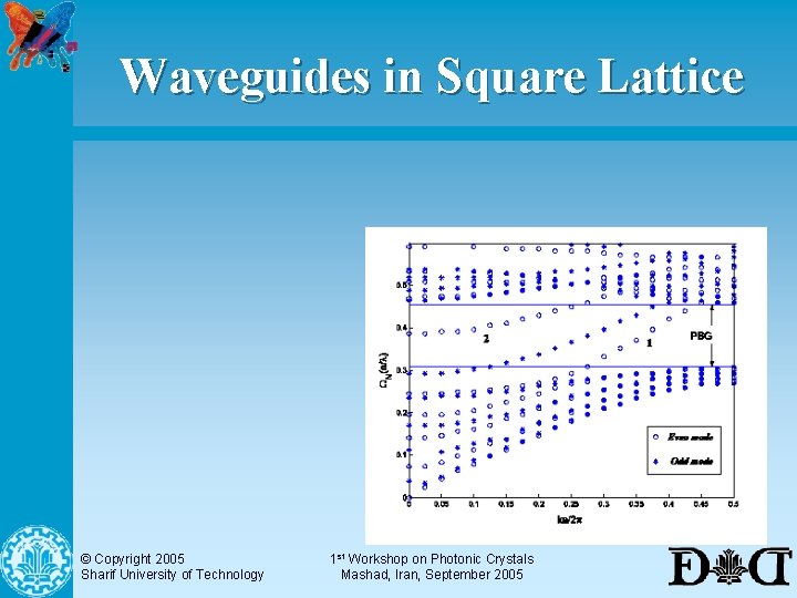
Waveguides in Square Lattice n Two rows of rods are removed from a bulk photonic crystal © Copyright 2005 Sharif University of Technology 1 st Workshop on Photonic Crystals Mashad, Iran, September 2005

Waveguides in Square Lattice © Copyright 2005 Sharif University of Technology 1 st Workshop on Photonic Crystals Mashad, Iran, September 2005

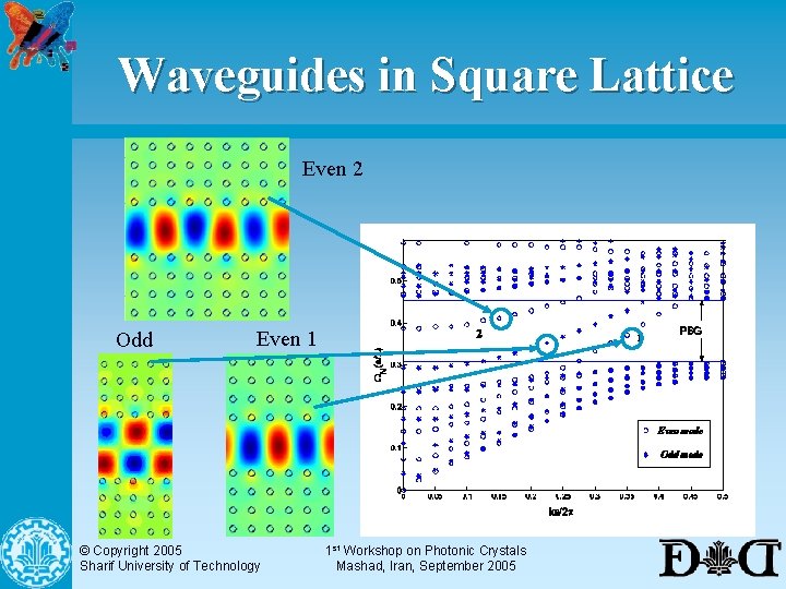
Waveguides in Square Lattice Even 2 Odd Even 1 © Copyright 2005 Sharif University of Technology 1 st Workshop on Photonic Crystals Mashad, Iran, September 2005

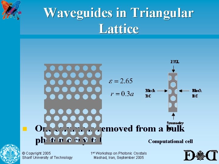
Waveguides in Triangular Lattice n One column is removed from a bulk Computational cell photonic crystal © Copyright 2005 Sharif University of Technology 1 st Workshop on Photonic Crystals Mashad, Iran, September 2005

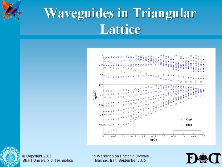
Waveguides in Triangular Lattice © Copyright 2005 Sharif University of Technology 1 st Workshop on Photonic Crystals Mashad, Iran, September 2005

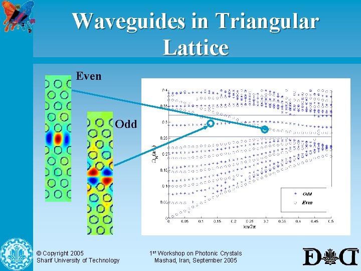
Waveguides in Triangular Lattice Even Odd © Copyright 2005 Sharif University of Technology 1 st Workshop on Photonic Crystals Mashad, Iran, September 2005

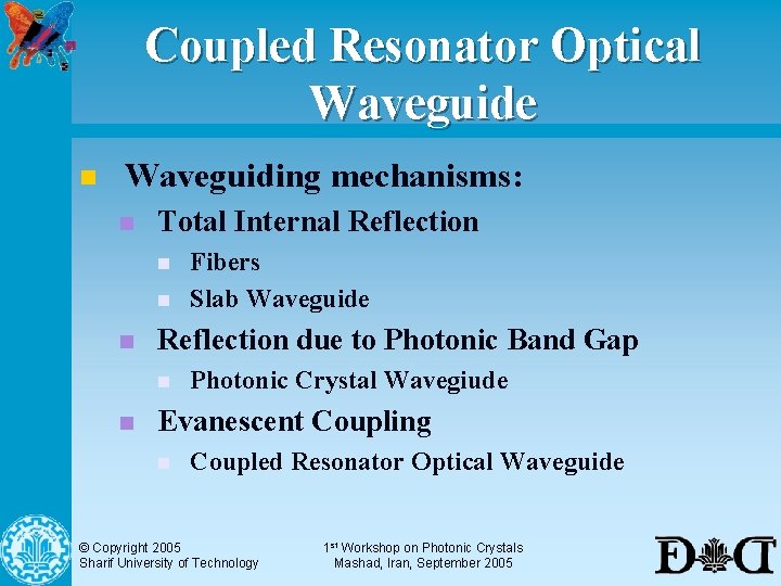
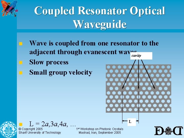
Coupled Resonator Optical Waveguide n Waveguiding mechanisms: n Total Internal Reflection n Reflection due to Photonic Band Gap n n Fibers Slab Waveguide Photonic Crystal Wavegiude Evanescent Coupling n Coupled Resonator Optical Waveguide © Copyright 2005 Sharif University of Technology 1 st Workshop on Photonic Crystals Mashad, Iran, September 2005

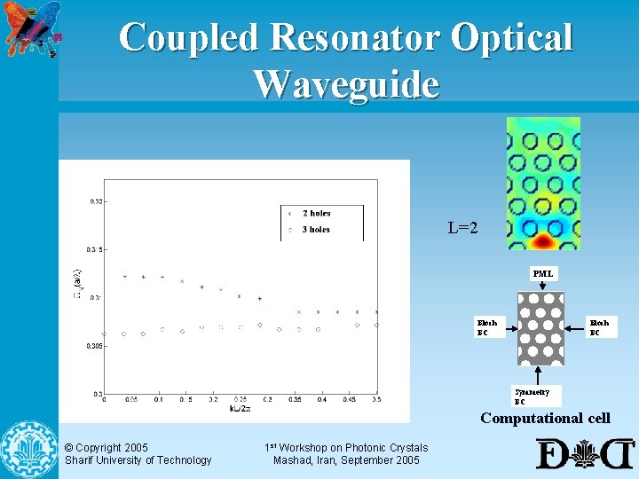
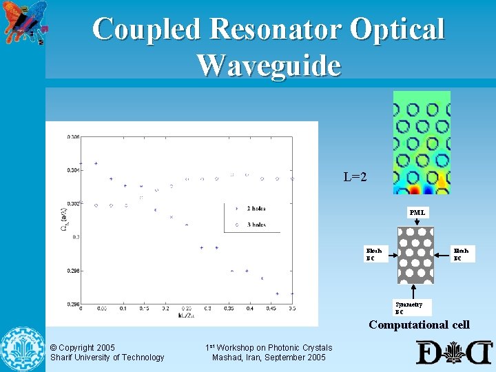
Coupled Resonator Optical Waveguide n Wave is coupled from one resonator to the adjacent through evanescent waves. cavity Slow process Small group velocity n L = 2 a, 3 a, 4 a, … n n © Copyright 2005 Sharif University of Technology 1 st Workshop on Photonic Crystals Mashad, Iran, September 2005 L

Coupled Resonator Optical Waveguide L=2 PML Bloch BC n Symmetry BC Odd Mode © Copyright 2005 Sharif University of Technology Bloch BC Computational cell 1 st Workshop on Photonic Crystals Mashad, Iran, September 2005

Coupled Resonator Optical Waveguide L=2 PML Bloch BC n Symmetry BC Even Mode © Copyright 2005 Sharif University of Technology Bloch BC Computational cell 1 st Workshop on Photonic Crystals Mashad, Iran, September 2005

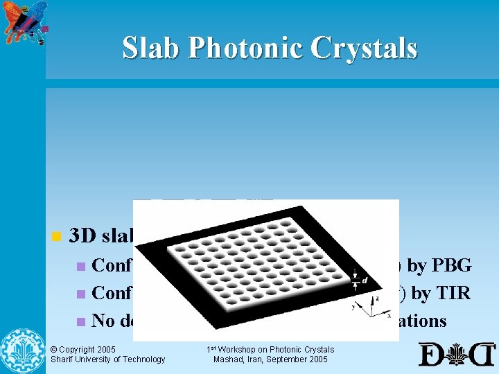
Slab Photonic Crystals n 3 D slab photonic crystal slabs: Confinement in the plane of slab (x-y) by PBG n Confinement perpendicular to slab (z) by TIR n No decoupling to TE and TM polarizations n © Copyright 2005 Sharif University of Technology 1 st Workshop on Photonic Crystals Mashad, Iran, September 2005

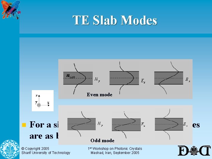
TE Slab Modes Even mode n For a simple slab waveguide mode profiles are as below Odd mode © Copyright 2005 Sharif University of Technology 1 st Workshop on Photonic Crystals Mashad, Iran, September 2005

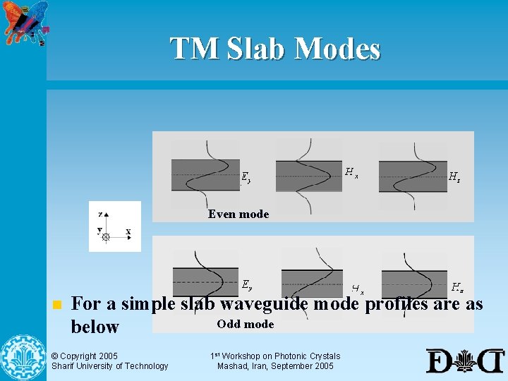
TM Slab Modes Even mode n For a simple slab waveguide mode profiles are as Odd mode below © Copyright 2005 Sharif University of Technology 1 st Workshop on Photonic Crystals Mashad, Iran, September 2005

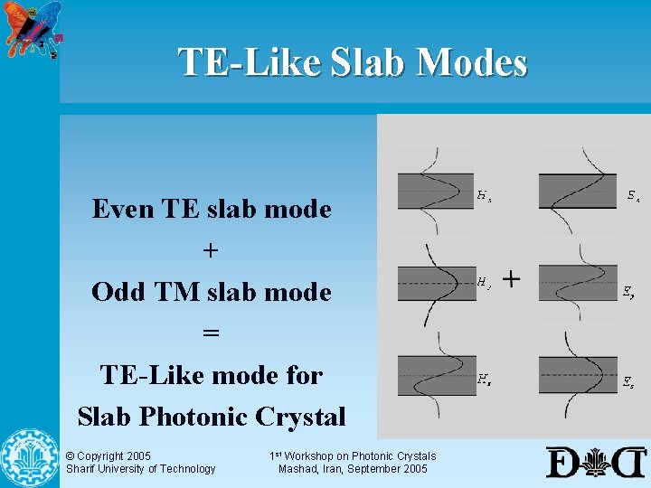
TE-Like Slab Modes Even TE slab mode + Odd TM slab mode = TE-Like mode for Slab Photonic Crystal © Copyright 2005 Sharif University of Technology 1 st Workshop on Photonic Crystals Mashad, Iran, September 2005

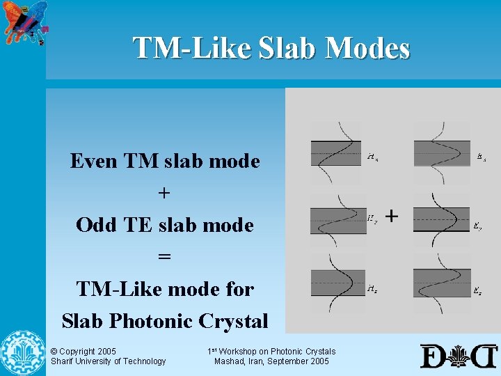
TM-Like Slab Modes Even TM slab mode + Odd TE slab mode = TM-Like mode for Slab Photonic Crystal © Copyright 2005 Sharif University of Technology 1 st Workshop on Photonic Crystals Mashad, Iran, September 2005

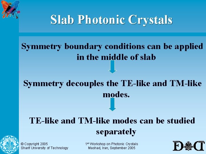
Slab Photonic Crystals Symmetry boundary conditions can be applied in the middle of slab Symmetry decouples the TE-like and TM-like modes can be studied separately © Copyright 2005 Sharif University of Technology 1 st Workshop on Photonic Crystals Mashad, Iran, September 2005

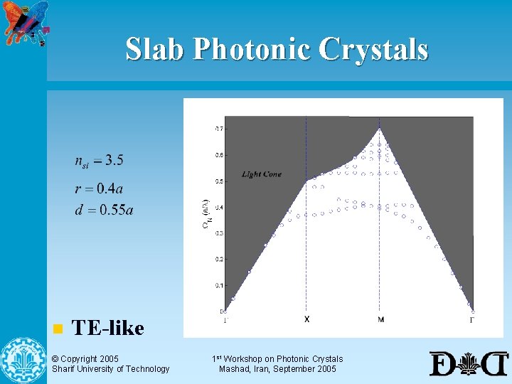
Slab Photonic Crystals n TE-like © Copyright 2005 Sharif University of Technology 1 st Workshop on Photonic Crystals Mashad, Iran, September 2005

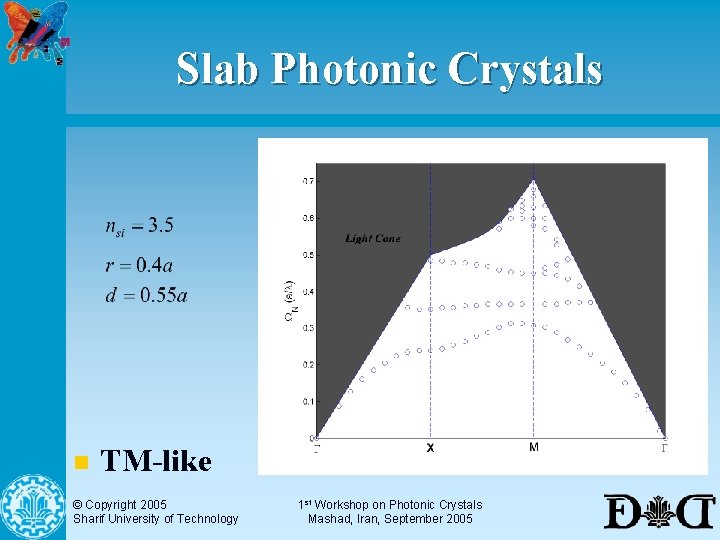
Slab Photonic Crystals n TM-like © Copyright 2005 Sharif University of Technology 1 st Workshop on Photonic Crystals Mashad, Iran, September 2005

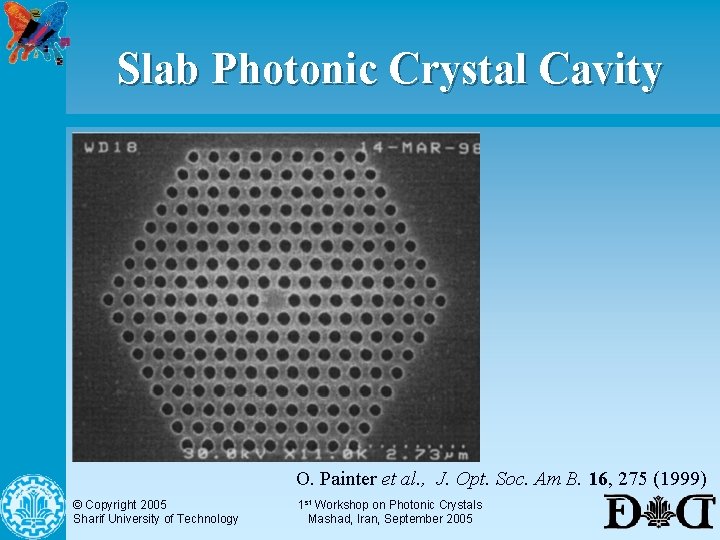
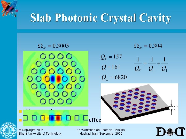
Slab Photonic Crystal Cavity O. Painter et al. , J. Opt. Soc. Am B. 16, 275 (1999) © Copyright 2005 Sharif University of Technology 1 st Workshop on Photonic Crystals Mashad, Iran, September 2005

Slab Photonic Crystal Cavity n n Even mode : 3 D : © Copyright 2005 Sharif University of Technology 2 D + effective index : 1 st Workshop on Photonic Crystals Mashad, Iran, September 2005

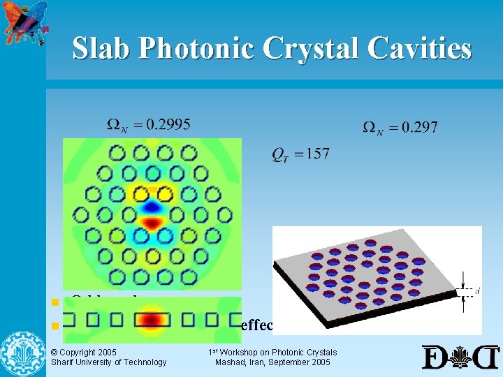
Slab Photonic Crystal Cavities n n Odd mode : 3 D : © Copyright 2005 Sharif University of Technology 2 D + effective index : 1 st Workshop on Photonic Crystals Mashad, Iran, September 2005

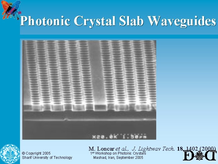
Photonic Crystal Slab Waveguides © Copyright 2005 Sharif University of Technology M. Loncar et al. , J. Lightwav Tech. 18, 1402 (2000) 1 st Workshop on Photonic Crystals Mashad, Iran, September 2005

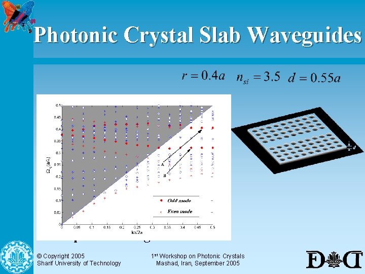
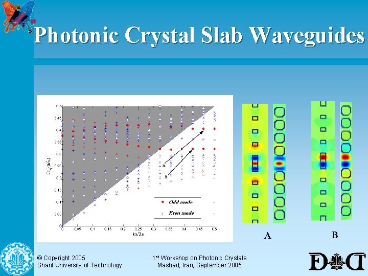
Photonic Crystal Slab Waveguides n Dispersion Diagram © Copyright 2005 Sharif University of Technology 1 st Workshop on Photonic Crystals Mashad, Iran, September 2005

Photonic Crystal Slab Waveguides n A Mode Profiles © Copyright 2005 Sharif University of Technology 1 st Workshop on Photonic Crystals Mashad, Iran, September 2005 B

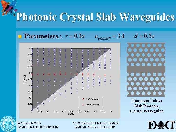
Photonic Crystal Slab Waveguides n Parameters : Triangular Lattice Slab Photonic Crystal Waveguide © Copyright 2005 Sharif University of Technology 1 st Workshop on Photonic Crystals Mashad, Iran, September 2005

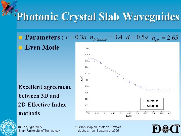
Photonic Crystal Slab Waveguides n n Parameters : Even Mode Excellent agreement between 3 D and 2 D Effective Index methods © Copyright 2005 Sharif University of Technology 1 st Workshop on Photonic Crystals Mashad, Iran, September 2005

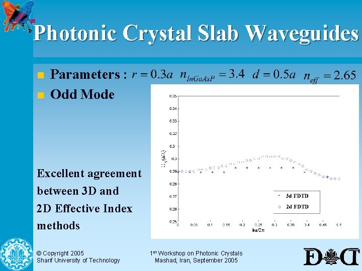
Photonic Crystal Slab Waveguides n n Parameters : Odd Mode Excellent agreement between 3 D and 2 D Effective Index methods © Copyright 2005 Sharif University of Technology 1 st Workshop on Photonic Crystals Mashad, Iran, September 2005

Conclusions n n n Plane Wave Expansion method has been coded and various results were obtained. Results of MATLAB code for 2 D single cell photonic crystal band structure computations are reliable and efficient enough. Performance of PWE is questionable beyond the abovementioned applications. © Copyright 2005 Sharif University of Technology 1 st Workshop on Photonic Crystals Mashad, Iran, September 2005

Conclusions n 2 D and 3 D FDTD codes are implemented in C++ and verified by comparing to reported results in literature in the following cases: Bandstructure of bulk photonic crystals n Resonant frequencies and Q-factor of different cavities n Dispersion diagram of different waveguides n… n © Copyright 2005 Sharif University of Technology 1 st Workshop on Photonic Crystals Mashad, Iran, September 2005

Thanks for your attention !