CHAPTER 9 PHOTONIC DEVICES Part 1 Photonic devices


- Slides: 35

CHAPTER 9: PHOTONIC DEVICES Part 1

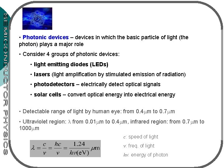
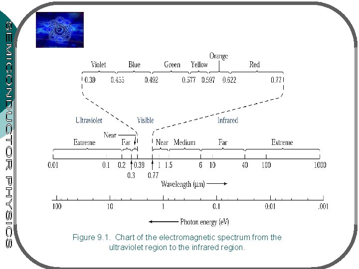
• Photonic devices – devices in which the basic particle of light (the photon) plays a major role • Consider 4 groups of photonic devices: • light emitting diodes (LEDs) • lasers (light amplification by stimulated emission of radiation) • photodetectors – electrically detect optical signals • solar cells – convert optical energy into electrical energy • Detectable range of light by human eye: from 0. 4 m to 0. 7 m • Ultraviolet region: from 0. 01 m to 0. 4 m, infrared region: from 0. 7 m to 1000 m c: speed of light v: freq. of light hv: energy of photon

Figure 9. 1. Chart of the electromagnetic spectrum from the ultraviolet region to the infrared region.

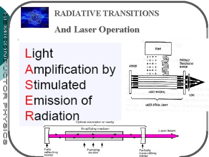
RADIATIVE TRANSITIONS And Laser Operation )

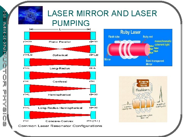
LASER MIRROR AND LASER PUMPING

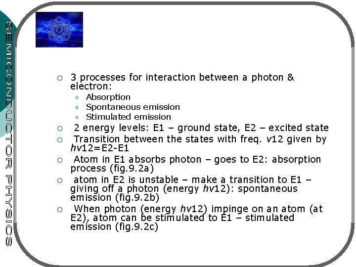
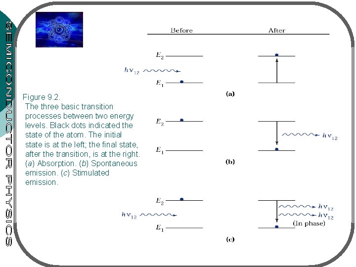
¡ 3 processes for interaction between a photon & electron: l l l ¡ ¡ ¡ Absorption Spontaneous emission Stimulated emission 2 energy levels: E 1 – ground state, E 2 – excited state Transition between the states with freq. v 12 given by hv 12=E 2 -E 1 Atom in E 1 absorbs photon – goes to E 2: absorption process (fig. 9. 2 a) atom in E 2 is unstable – make a transition to E 1 – giving off a photon (energy hv 12): spontaneous emission (fig. 9. 2 b) When photon (energy hv 12) impinge on an atom (at E 2), atom can be stimulated to E 1 – stimulated emission (fig. 9. 2 c)

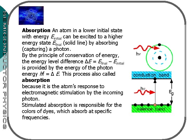
Absorption An atom in a lower initial state with energy Einitial can be excited to a higher energy state Efinal (solid line) by absorbing (capturing) a photon. By the principle of conservation of energy, the energy level difference ∆E = Efinal – Einitial is provided by the energy of the photon energy hf = ∆ E. This process also called absorption because it is the atom’s response to electromagnetic stimulation by the incoming photon. Stimulated absorption is responsible for the colors of dyes, which absorb at specific frequencies.

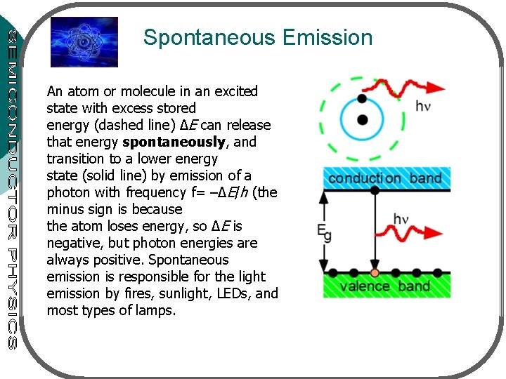
Spontaneous Emission An atom or molecule in an excited state with excess stored energy (dashed line) ∆E can release that energy spontaneously, and transition to a lower energy state (solid line) by emission of a photon with frequency f= –∆E/h (the minus sign is because the atom loses energy, so ∆E is negative, but photon energies are always positive. Spontaneous emission is responsible for the light emission by fires, sunlight, LEDs, and most types of lamps.

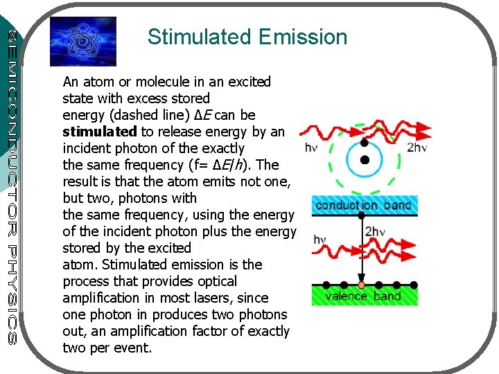
Stimulated Emission An atom or molecule in an excited state with excess stored energy (dashed line) ∆E can be stimulated to release energy by an incident photon of the exactly the same frequency (f= ∆E/h). The result is that the atom emits not one, but two, photons with the same frequency, using the energy of the incident photon plus the energy stored by the excited atom. Stimulated emission is the process that provides optical amplification in most lasers, since one photon in produces two photons out, an amplification factor of exactly two per event.

Figure 9. 2. The three basic transition processes between two energy levels. Black dots indicated the state of the atom. The initial state is at the left; the final state, after the transition, is at the right. (a) Absorption. (b) Spontaneous emission. (c) Stimulated emission.

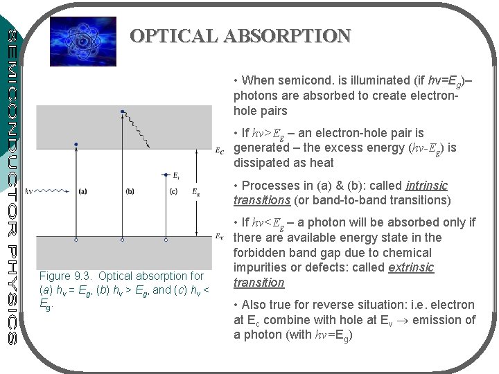
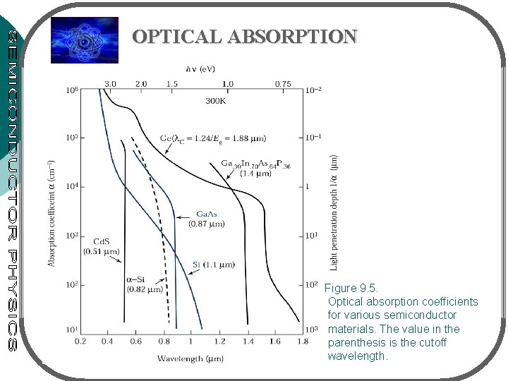
OPTICAL ABSORPTION • When semicond. is illuminated (if hv=Eg)– photons are absorbed to create electronhole pairs • If hv>Eg – an electron-hole pair is generated – the excess energy (hv-Eg) is dissipated as heat • Processes in (a) & (b): called intrinsic transitions (or band-to-band transitions) Figure 9. 3. Optical absorption for (a) hv = Eg, (b) hv > Eg, and (c) hv < E g. • If hv<Eg – a photon will be absorbed only if there available energy state in the forbidden band gap due to chemical impurities or defects: called extrinsic transition • Also true for reverse situation: i. e. electron at Ec combine with hole at Ev emission of a photon (with hv=Eg)

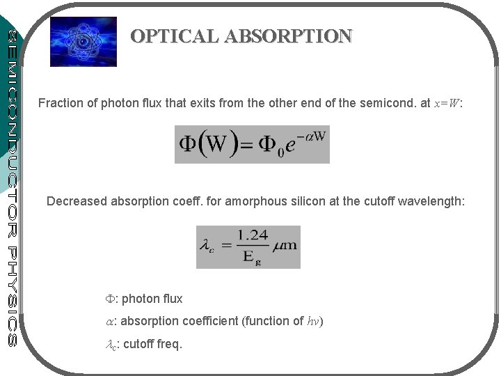
OPTICAL ABSORPTION Fraction of photon flux that exits from the other end of the semicond. at x=W: Decreased absorption coeff. for amorphous silicon at the cutoff wavelength: : photon flux : absorption coefficient (function of hv) c: cutoff freq.

OPTICAL ABSORPTION Figure 9. 5. Optical absorption coefficients for various semiconductor materials. The value in the parenthesis is the cutoff wavelength.

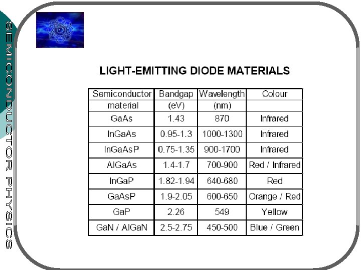
LED Stands for light emitting diode. ¡ Semiconductor device: ¡ l l p-n junction forward-biased. current ¡ emits incoherent narrow spectrum light ¡ (due to recombination in transition region near the junction. ) ¡ Color of the emitted light depends on the chemical of the semiconducting material used. ¡ (Near-ultraviolet, visible or infrared. )

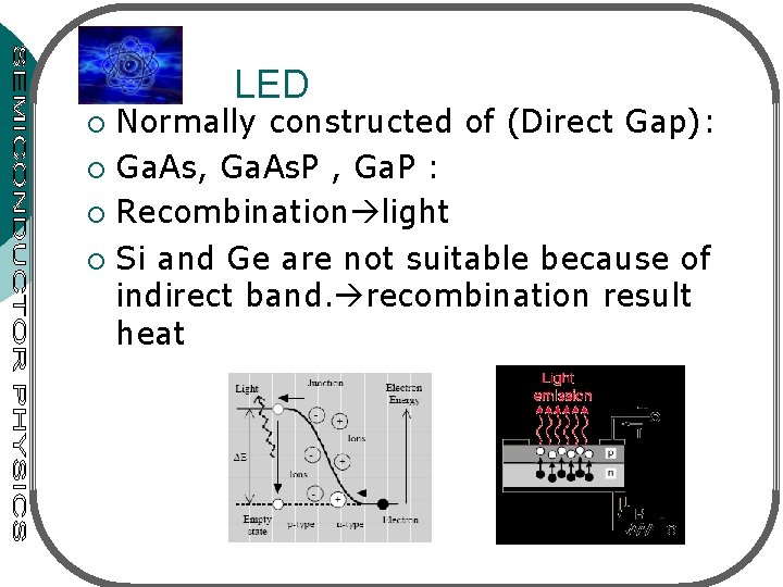
LED Normally constructed of (Direct Gap): ¡ Ga. As, Ga. As. P , Ga. P : ¡ Recombination light ¡ Si and Ge are not suitable because of indirect band. recombination result heat ¡

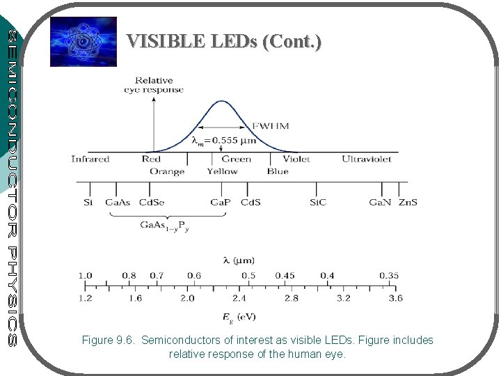
LIGHT EMITTING DIODE (LED) LEDs are p-n junctions that can emit spontaneous radiation in ultraviolet, visible or infrared regions A & B: group III VISIBLE LEDs C & D: group V x & y: mole fraction • max. sensitivity of the eye: at 0. 555 m • eye response – nearly ‘ 0’ at the visible spectrum of 0. 4 & 0. 7 m • Eye only sensitive to light with photon energy hv 1. 8 e. V (or 0. 7 m) – semicond. of interest must have larger energy bandgap • See fig. 9. 6 – the most important materials for visible LEDs: alloy Ga. As 1 -y. Py & Gax. In 1 -x. N III-V compound system • Notation: Ax. B 1 -x. C or AC 1 -y. Dy for ternary (3 elements) • Ax. B 1 -x. Cy. D 1 -y for quarternary (4 elements)


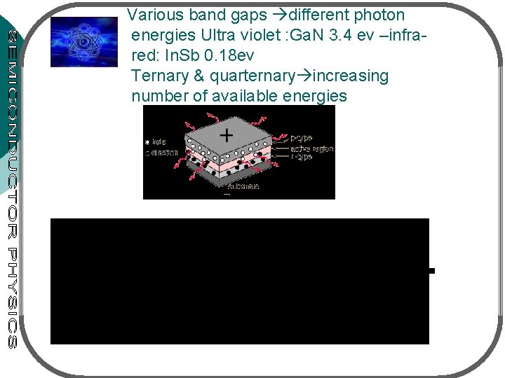
Various band gaps different photon energies Ultra violet : Ga. N 3. 4 ev –infrared: In. Sb 0. 18 ev Ternary & quarternary increasing number of available energies

VISIBLE LEDs (Cont. ) Figure 9. 6. Semiconductors of interest as visible LEDs. Figure includes relative response of the human eye.

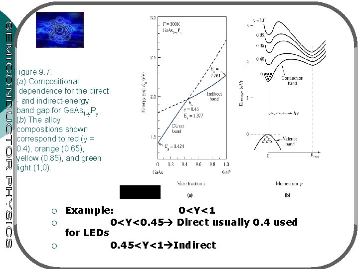
Figure 9. 7. (a) Compositional dependence for the direct - and indirect-energy band gap for Ga. As 1 -y. Py. (b) The alloy compositions shown correspond to red (y = 0. 4), orange (0. 65), yellow (0. 85), and green light (1, 0). ¡ ¡ ¡ Example: 0<Y<1 0<Y<0. 45 Direct usually 0. 4 used for LEDs 0. 45<Y<1 Indirect

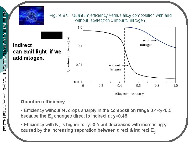
Figure 9. 8. Quantum efficiency versus alloy composition with and without isoelectronic impurity nitrogen. Indirect can emit light if we add nitogen. Quantum efficiency • Efficiency without N 2 drops sharply in the composition range 0. 4<y<0. 5 because the Eg changes direct to indirect at y=0. 45 • Efficiency with N 2 is higher for y>0. 5 but decreases with increasing y – caused by the increasing separation between direct & indirect Eg

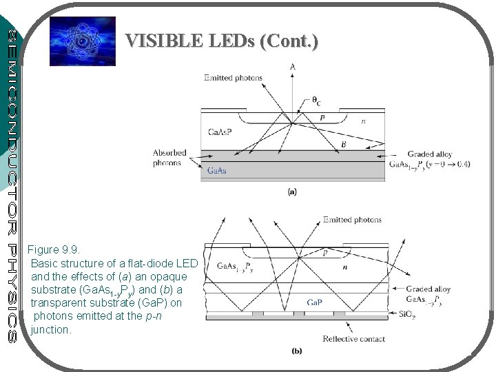
VISIBLE LEDs (Cont. ) • Fig. 9. 9(a) – Direct-Eg LED emits red light, fabricated on Ga. As substrate • Fig. 9. 9(b) – Indirect-Eg LED emits orange, yellow or green light, fabricated on Ga. P substrates • For high-brightness blue LEDs (0. 455 -0. 492 m) – II-VI compounds (Zn. Se), III-V (Ga. N), IV-IV (Si. C) • II-IV based devices – have short lifetimes (not good) • Si. C (indirect Eg) low brightness • Direct Eg: Ga. N (Eg=3. 44 e. V), III-V semicond. (Al. Ga. In. N) • High quality Ga. N has been grown on sapphire (insulator) substrate

VISIBLE LEDs (Cont. ) Figure 9. 9. Basic structure of a flat-diode LED and the effects of (a) an opaque substrate (Ga. As 1 -y. Py) and (b) a transparent substrate (Ga. P) on photons emitted at the p-n junction.

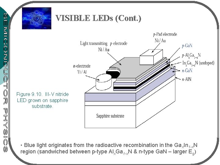
VISIBLE LEDs (Cont. ) Figure 9. 10. III-V nitride LED grown on sapphire substrate. • Blue light originates from the radioactive recombination in the Gax. In 1 -x. N region (sandwiched between p-type Alx. Ga 1 -x. N & n-type Ga. N – larger Eg)

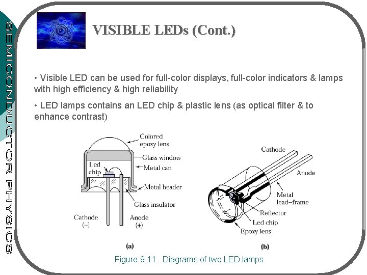
VISIBLE LEDs (Cont. ) • Visible LED can be used for full-color displays, full-color indicators & lamps with high efficiency & high reliability • LED lamps contains an LED chip & plastic lens (as optical filter & to enhance contrast) Figure 9. 11. Diagrams of two LED lamps.

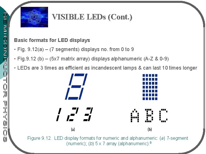
VISIBLE LEDs (Cont. ) Basic formats for LED displays • Fig. 9. 12(a) – (7 segments) displays no. from 0 to 9 • Fig. 9. 12 (b) – (5 x 7 matrix array) displays alphanumeric (A-Z & 0 -9) • LEDs are 3 times as efficient as incandescent lamps & can last 10 times longer Figure 9. 12. LED display formats for numeric and alphanumeric: (a) 7 -segment (numeric); (b) 5 x 7 array (alphanumeric). 8

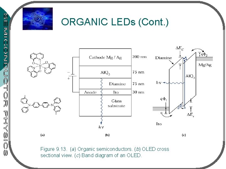
ORGANIC LEDs • Application: multicolor, large-area flat panel display (attributes low power consumption & excellent emissive quality with a wide viewing angle • Fig. 9. 13(a) – 2 representative organic semicond. ([Al. Q 3] & aromatic diamine) • Fig. 9. 13(b) – transparent substrate – transparent anode (ITO) – diamine (hole transport) – Al. Q 3 (electron transport) – cathode • Fig. 9. 13(c) – electrons are injected from cathode toward heterojunction interface (Al. Q 3/diamine) – holes are injected from anode toward the interface

ORGANIC LEDs (Cont. ) Figure 9. 13. (a) Organic semiconductors. (b) OLED cross sectional view. (c) Band diagram of an OLED.

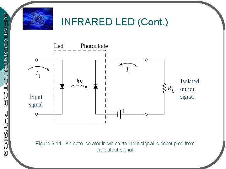
INFRARED LED Application 1: opto-isolators (input or control signal is decoupled from the output • Fig. 9. 14 – opto-isolator having infrared LED (light source) & photodiode (detector) • Input signal applied to LED will generate light detected by the photodiode light is converted back to an electrical signal as I that flows thru load resistor • Application 2: communication system (transmission of an optical signal thru optical fiber) • Optical fiber – a waveguide at optical frequencies

INFRARED LED (Cont. ) Figure 9. 14. An opto-isolator in which an input signal is decoupled from the output signal.

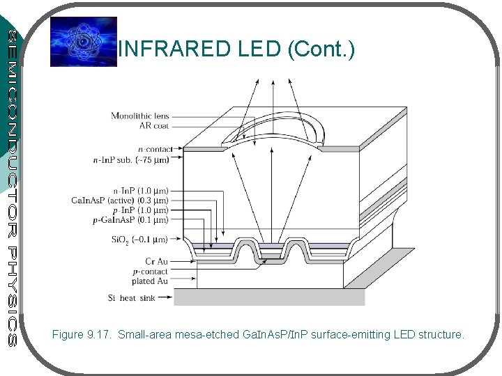
INFRARED LED (Cont. ) • The surface-emitting infrared In. Ga. As. P LED – for optical fiber communication • Light emitted from the central surface area & coupled into the optical fiber • Heterojunctions – • increase efficiency (from the confinement of the carriers by the In. P higher Eg) • also serve as an optical window to the emitted radiation (higher Eg – confining layers do not absorb radiation from the lower Eg – emitting region)

INFRARED LED (Cont. ) Figure 9. 17. Small-area mesa-etched Ga. In. As. P/In. P surface-emitting LED structure.

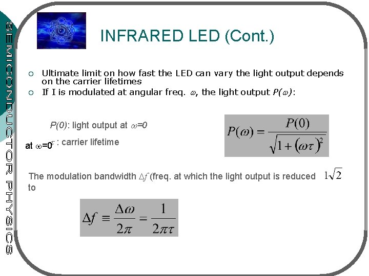
INFRARED LED (Cont. ) ¡ ¡ Ultimate limit on how fast the LED can vary the light output depends on the carrier lifetimes If I is modulated at angular freq. , the light output P( ): P(0): light output at =0 : carrier lifetime The modulation bandwidth f (freq. at which the light output is reduced to

Test 2 will be on Thursday 16 th Oct. 2008 @ K. Perlis (DKP 1) 8. 30 pm – 9. 30 pm

The presentation of Miniprojects (with Assignments) will be on Wednesday 22/10/2008 @ K. Perlis (DKP 1) 8 -10 am The attendance is Compulsory