Photonic Crystals Photonic Crystals From Wikipedia Photonic Crystals
- Slides: 53

Photonic Crystals

Photonic Crystals From Wikipedia: “Photonic Crystals are periodic optical nanostructures that are designed to affect the motion of photons in a similar way that periodicity of a semiconductor crystal affects the motion of electrons. Photonic crystals occur in nature and in various forms have been studied scientifically for the last 100 years”.

Wikipedia Continued • “Photonic crystals are composed of periodic dielectric or metallo-dielectric nanostructures that affect the propagation of electromagnetic waves (EM) in the same way as the periodic potential in a crystal affects the electron motion by defining allowed and forbidden electronic energy bands. Photonic crystals contain regularly repeating internal regions of high and low dielectric constant. Photons (as waves) propagate through this structure - or not - depending on their wavelength. Wavelengths of light that are allowed to travel are known as modes, and groups of allowed modes form bands. Disallowed bands of wavelengths are called photonic band gaps. This gives rise to distinct optical phenomena such as inhibition of spontaneous emission, high-reflecting omnidirectional mirrors and low-loss-waveguides, amongst others. • Since the basic physical phenomenon is based on diffraction, the periodicity of the photonic crystal structure has to be of the same length-scale as half the wavelength of the EM waves i. e. ~350 nm (blue) to 700 nm (red) for photonic crystals operating in the visible part of the spectrum - the repeating regions of high and low dielectric constants have to be of this dimension. This makes the fabrication of optical photonic crystals cumbersome and complex.

Photonic Crystals: A New Frontier in Modern Optics MARIAN FLORESCU NASA Jet Propulsion Laboratory California Institute of Technology

“ If only were possible to make materials in which electromagnetically waves cannot propagate at certain frequencies, all kinds of almost-magical things would happen” Sir John Maddox, Nature (1990)

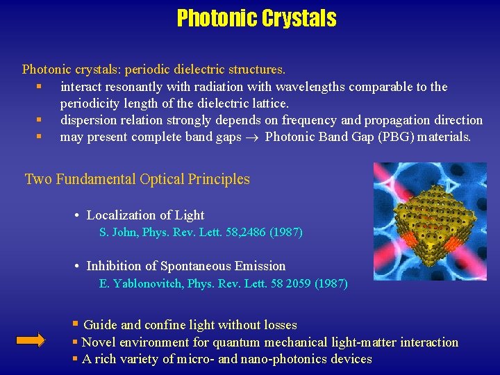
Photonic Crystals Photonic crystals: periodic dielectric structures. § § § interact resonantly with radiation with wavelengths comparable to the periodicity length of the dielectric lattice. dispersion relation strongly depends on frequency and propagation direction may present complete band gaps Photonic Band Gap (PBG) materials. Two Fundamental Optical Principles • Localization of Light S. John, Phys. Rev. Lett. 58, 2486 (1987) • Inhibition of Spontaneous Emission E. Yablonovitch, Phys. Rev. Lett. 58 2059 (1987) § Guide and confine light without losses § Novel environment for quantum mechanical light-matter interaction § A rich variety of micro- and nano-photonics devices

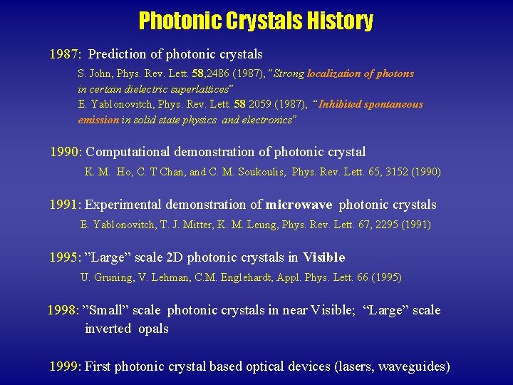
Photonic Crystals History 1987: Prediction of photonic crystals S. John, Phys. Rev. Lett. 58, 2486 (1987), “Strong localization of photons in certain dielectric superlattices” E. Yablonovitch, Phys. Rev. Lett. 58 2059 (1987), “Inhibited spontaneous emission in solid state physics and electronics” 1990: Computational demonstration of photonic crystal K. M. Ho, C. T Chan, and C. M. Soukoulis, Phys. Rev. Lett. 65, 3152 (1990) 1991: Experimental demonstration of microwave photonic crystals E. Yablonovitch, T. J. Mitter, K. M. Leung, Phys. Rev. Lett. 67, 2295 (1991) 1995: ”Large” scale 2 D photonic crystals in Visible U. Gruning, V. Lehman, C. M. Englehardt, Appl. Phys. Lett. 66 (1995) 1998: ”Small” scale photonic crystals in near Visible; “Large” scale inverted opals 1999: First photonic crystal based optical devices (lasers, waveguides)

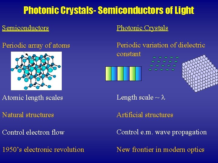
Photonic Crystals- Semiconductors of Light Semiconductors Photonic Crystals Periodic array of atoms Periodic variation of dielectric constant Atomic length scales Length scale ~ Natural structures Artificial structures Control electron flow Control e. m. wave propagation 1950’s electronic revolution New frontier in modern optics

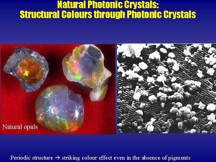
Natural Photonic Crystals: Structural Colours through Photonic Crystals Natural opals Periodic structure striking colour effect even in the absence of pigments

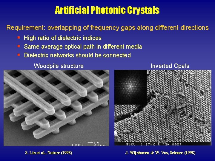
Artificial Photonic Crystals Requirement: overlapping of frequency gaps along different directions § § § High ratio of dielectric indices Same average optical path in different media Dielectric networks should be connected Woodpile structure S. Lin et al. , Nature (1998) Inverted Opals J. Wijnhoven & W. Vos, Science (1998)

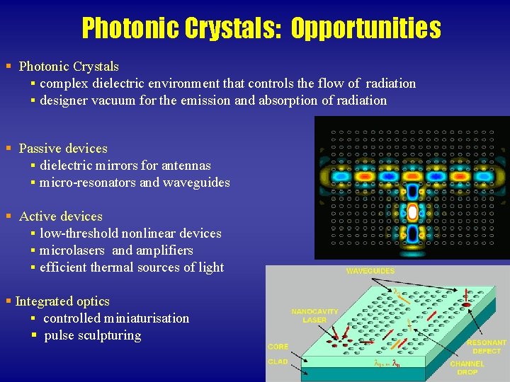
Photonic Crystals: Opportunities § Photonic Crystals § complex dielectric environment that controls the flow of radiation § designer vacuum for the emission and absorption of radiation § Passive devices § dielectric mirrors for antennas § micro-resonators and waveguides § Active devices § low-threshold nonlinear devices § microlasers and amplifiers § efficient thermal sources of light § Integrated optics § controlled miniaturisation § pulse sculpturing

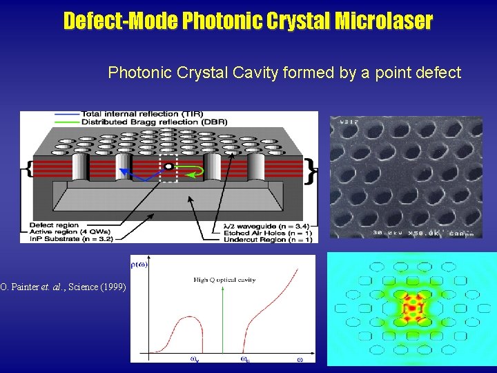
Defect-Mode Photonic Crystal Microlaser Photonic Crystal Cavity formed by a point defect O. Painter et. al. , Science (1999)

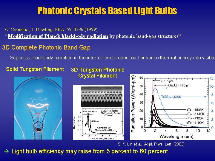
Photonic Crystals Based Light Bulbs C. Cornelius, J. Dowling, PRA 59, 4736 (1999) “Modification of Planck blackbody radiation by photonic band-gap structures” 3 D Complete Photonic Band Gap Suppress blackbody radiation in the infrared and redirect and enhance thermal energy into visible Solid Tungsten Filament 3 D Tungsten Photonic Crystal Filament S. Y. Lin et al. , Appl. Phys. Lett. (2003) Light bulb efficiency may raise from 5 percent to 60 percent

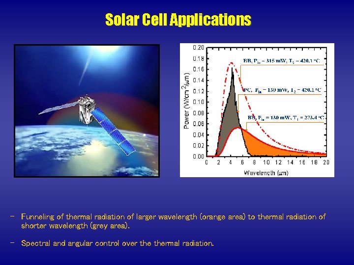
Solar Cell Applications – Funneling of thermal radiation of larger wavelength (orange area) to thermal radiation of shorter wavelength (grey area). – Spectral and angular control over thermal radiation.

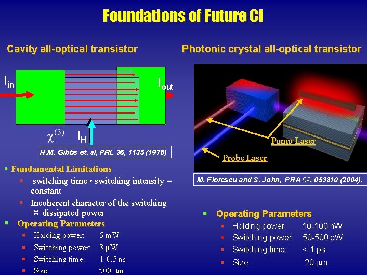
Foundations of Future CI Cavity all-optical transistor Iin Photonic crystal all-optical transistor Iout IH H. M. Gibbs et. al, PRL 36, 1135 (1976) § Fundamental Limitations § switching time • switching intensity = constant § Incoherent character of the switching dissipated power § Operating Parameters § § Holding power: 5 m. W Switching power: 3 µW Switching time: 1 -0. 5 ns Size: 500 m Pump Laser Probe Laser M. Florescu and S. John, PRA 69, 053810 (2004). § Operating Parameters § Holding power: 10 -100 n. W § Switching power: 50 -500 p. W § Switching time: < 1 ps § Size: 20 m

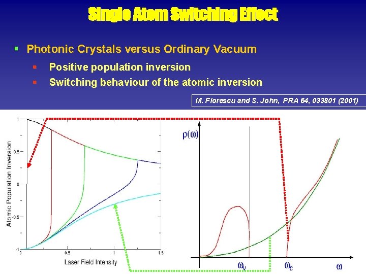
Single Atom Switching Effect § Photonic Crystals versus Ordinary Vacuum § § Positive population inversion Switching behaviour of the atomic inversion M. Florescu and S. John, PRA 64, 033801 (2001)

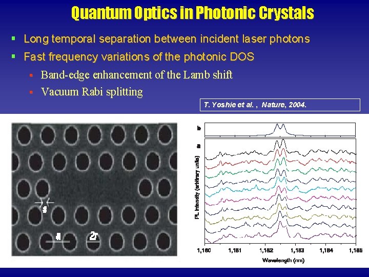
Quantum Optics in Photonic Crystals § Long temporal separation between incident laser photons § Fast frequency variations of the photonic DOS § § Band-edge enhancement of the Lamb shift Vacuum Rabi splitting T. Yoshie et al. , Nature, 2004.

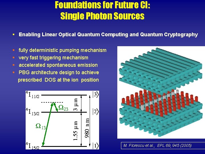
Foundations for Future CI: Single Photon Sources § Enabling Linear Optical Quantum Computing and Quantum Cryptography § § fully deterministic pumping mechanism very fast triggering mechanism accelerated spontaneous emission PBG architecture design to achieve prescribed DOS at the ion position M. Florescu et al. , EPL 69, 945 (2005)

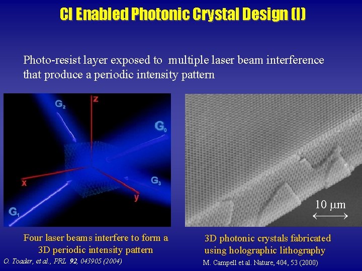
CI Enabled Photonic Crystal Design (I) Photo-resist layer exposed to multiple laser beam interference that produce a periodic intensity pattern 10 m Four laser beams interfere to form a 3 D periodic intensity pattern O. Toader, et al. , PRL 92, 043905 (2004) 3 D photonic crystals fabricated using holographic lithography M. Campell et al. Nature, 404, 53 (2000)

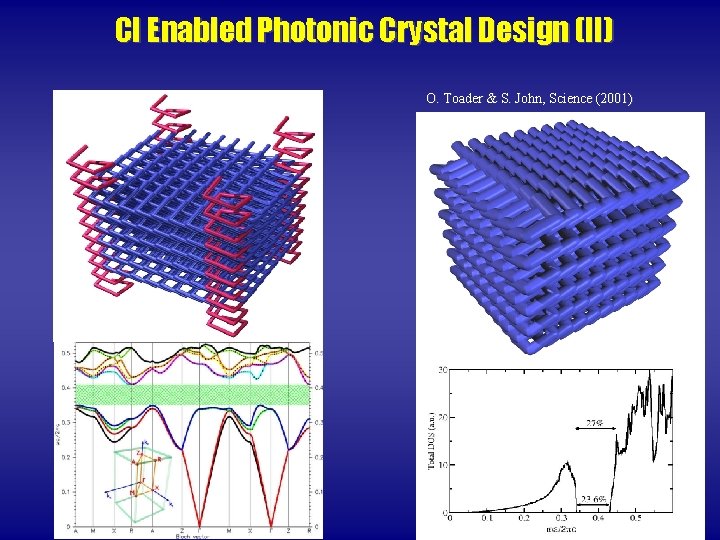
CI Enabled Photonic Crystal Design (II) O. Toader & S. John, Science (2001)

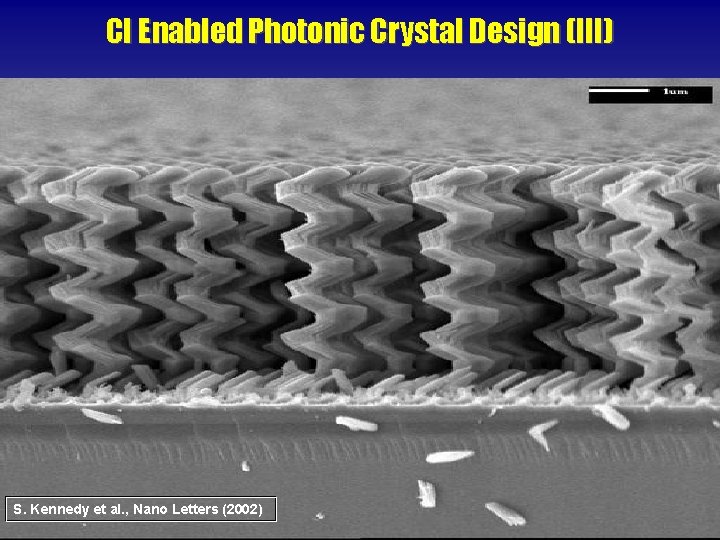
CI Enabled Photonic Crystal Design (III) S. Kennedy et al. , Nano Letters (2002)

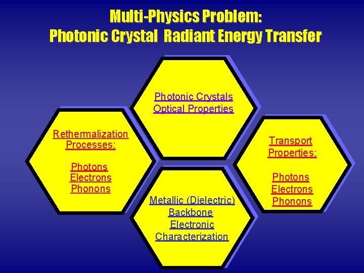
Multi-Physics Problem: Photonic Crystal Radiant Energy Transfer Photonic Crystals Optical Properties Rethermalization Processes: Transport Properties: Photons Electrons Phonons Metallic (Dielectric) Backbone Electronic Characterization Photons Electrons Phonons

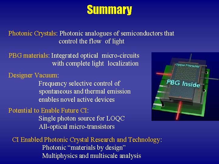
Summary Photonic Crystals: Photonic analogues of semiconductors that control the flow of light PBG materials: Integrated optical micro-circuits with complete light localization Designer Vacuum: Frequency selective control of spontaneous and thermal emission enables novel active devices Potential to Enable Future CI: Single photon source for LOQC All-optical micro-transistors CI Enabled Photonic Crystal Research and Technology: Photonic “materials by design” Multiphysics and multiscale analysis

Wikipedia Continued • “Photonic crystals are composed of periodic dielectric or metallo-dielectric nanostructures that affect the propagation of electromagnetic waves (EM) in the same way as the periodic potential in a crystal affects the electron motion by defining allowed and forbidden electronic energy bands. Photonic crystals contain regularly repeating internal regions of high and low dielectric constant. Photons (as waves) propagate through this structure - or not - depending on their wavelength. Wavelengths of light that are allowed to travel are known as modes, and groups of allowed modes form bands. Disallowed bands of wavelengths are called photonic band gaps. This gives rise to distinct optical phenomena such as inhibition of spontaneous emission, high-reflecting omnidirectional mirrors and low-loss-waveguides, amongst others. • Since the basic physical phenomenon is based on diffraction, the periodicity of the photonic crystal structure has to be of the same length-scale as half the wavelength of the EM waves i. e. ~350 nm (blue) to 700 nm (red) for photonic crystals operating in the visible part of the spectrum - the repeating regions of high and low dielectric constants have to be of this dimension. This makes the fabrication of optical photonic crystals cumbersome and complex.

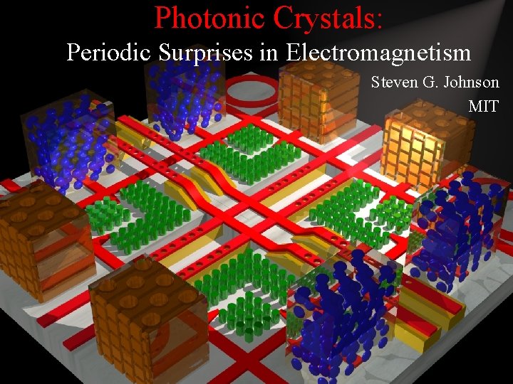
Photonic Crystals: Periodic Surprises in Electromagnetism Steven G. Johnson MIT

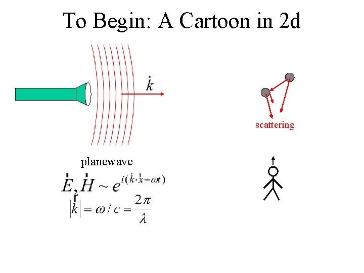
To Begin: A Cartoon in 2 d scattering planewave

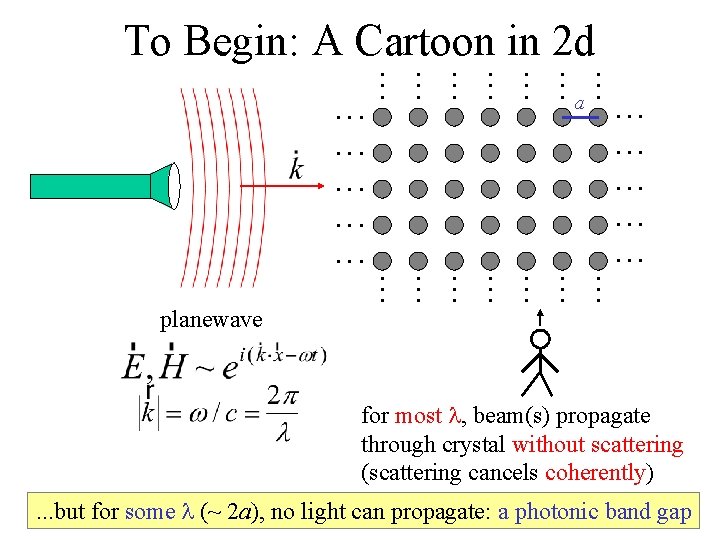
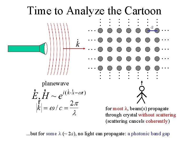
To Begin: A Cartoon in 2 d a • • • • • • • • • • • • • • • • • • planewave for most , beam(s) propagate through crystal without scattering (scattering cancels coherently). . . but for some (~ 2 a), no light can propagate: a photonic band gap

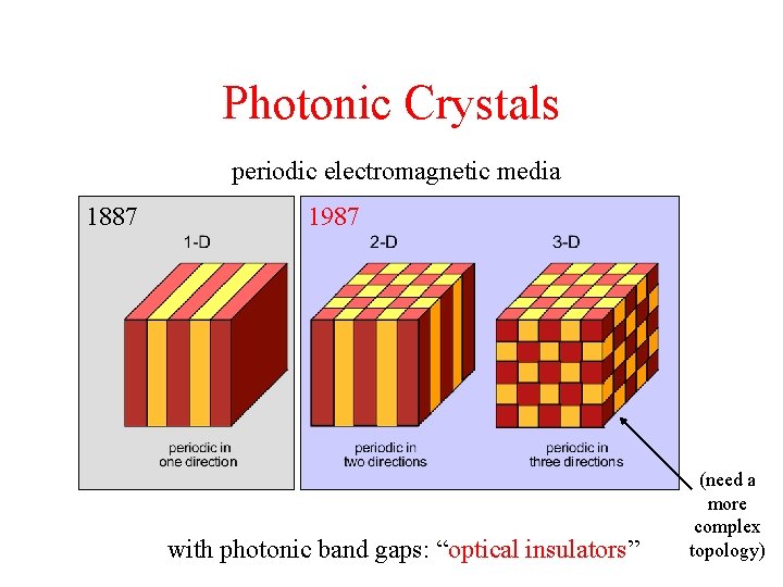
Photonic Crystals periodic electromagnetic media 1887 1987 with photonic band gaps: “optical insulators” (need a more complex topology)

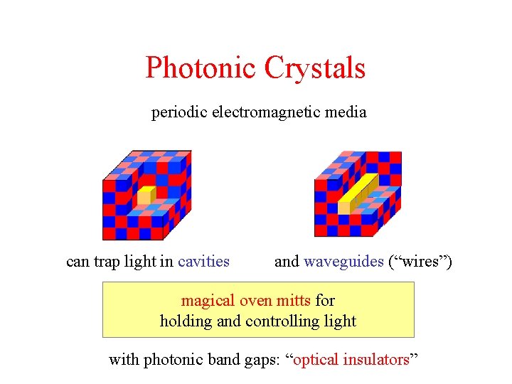
Photonic Crystals periodic electromagnetic media can trap light in cavities and waveguides (“wires”) magical oven mitts for holding and controlling light with photonic band gaps: “optical insulators”

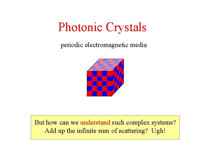
Photonic Crystals periodic electromagnetic media But how can we understand such complex systems? Add up the infinite sum of scattering? Ugh!

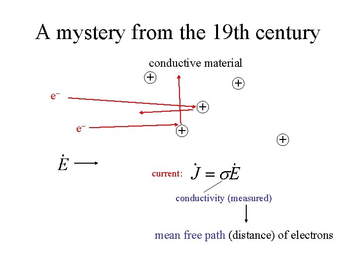
A mystery from the 19 th century conductive material + + e– + + current: conductivity (measured) mean free path (distance) of electrons

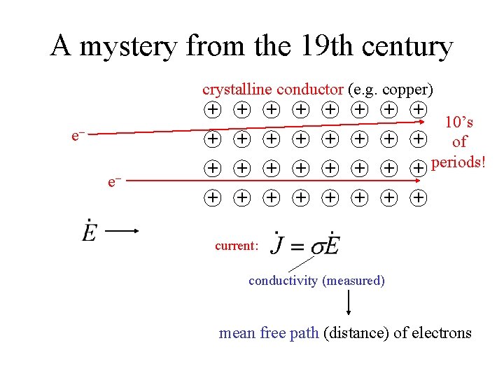
A mystery from the 19 th century crystalline conductor (e. g. copper) + + + + e– e– + + + + 10’s + of + periods! + + + + current: conductivity (measured) mean free path (distance) of electrons

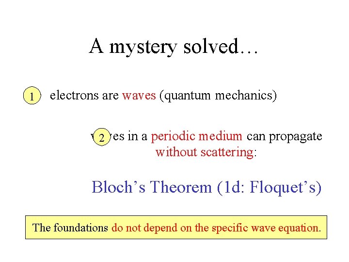
A mystery solved… 1 electrons are waves (quantum mechanics) waves in a periodic medium can propagate 2 without scattering: Bloch’s Theorem (1 d: Floquet’s) The foundations do not depend on the specific wave equation.

Time to Analyze the Cartoon a • • • • • • • • • • • • • • • • • • planewave for most , beam(s) propagate through crystal without scattering (scattering cancels coherently). . . but for some (~ 2 a), no light can propagate: a photonic band gap

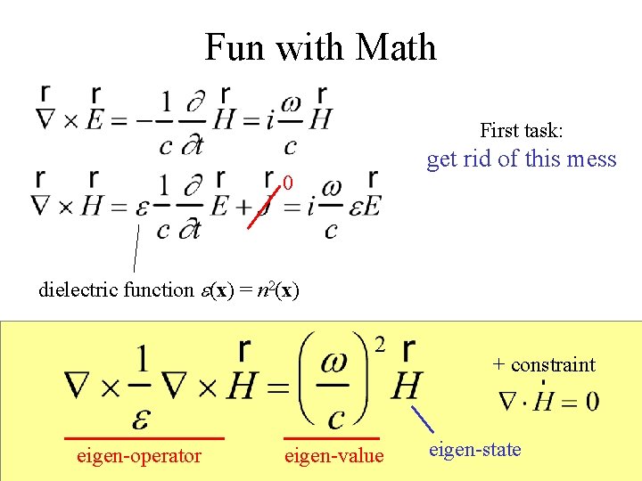
Fun with Math First task: 0 get rid of this mess dielectric function e(x) = n 2(x) + constraint eigen-operator eigen-value eigen-state

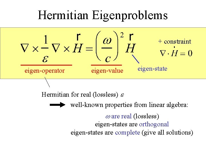
Hermitian Eigenproblems + constraint eigen-operator eigen-value eigen-state Hermitian for real (lossless) e well-known properties from linear algebra: w are real (lossless) eigen-states are orthogonal eigen-states are complete (give all solutions)

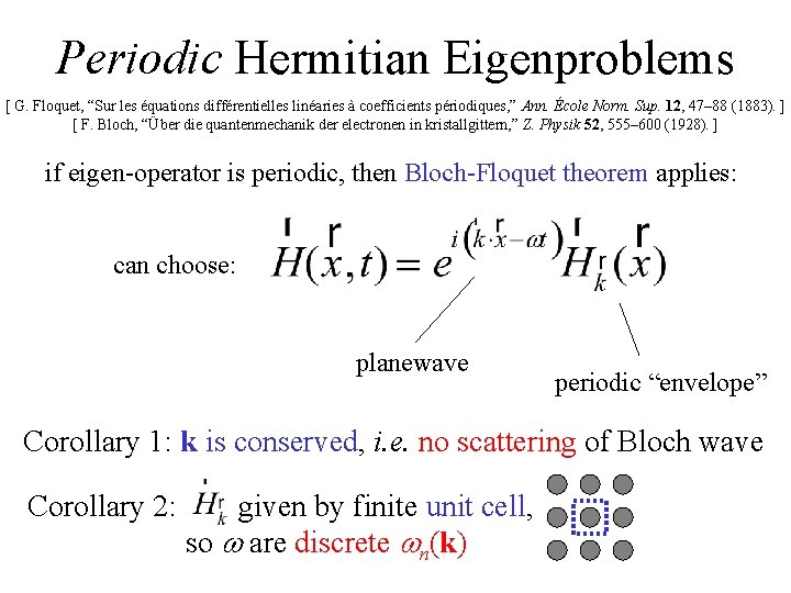
Periodic Hermitian Eigenproblems [ G. Floquet, “Sur les équations différentielles linéaries à coefficients périodiques, ” Ann. École Norm. Sup. 12, 47– 88 (1883). ] [ F. Bloch, “Über die quantenmechanik der electronen in kristallgittern, ” Z. Physik 52, 555– 600 (1928). ] if eigen-operator is periodic, then Bloch-Floquet theorem applies: can choose: planewave periodic “envelope” Corollary 1: k is conserved, i. e. no scattering of Bloch wave Corollary 2: given by finite unit cell, so w are discrete wn(k)

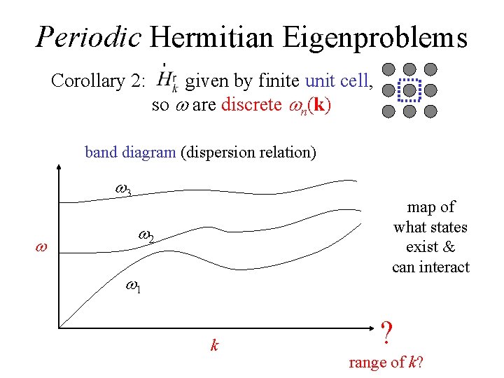
Periodic Hermitian Eigenproblems Corollary 2: given by finite unit cell, so w are discrete wn(k) band diagram (dispersion relation) w 3 w map of what states exist & can interact w 2 w 1 k ? range of k?

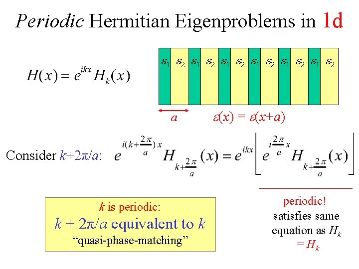
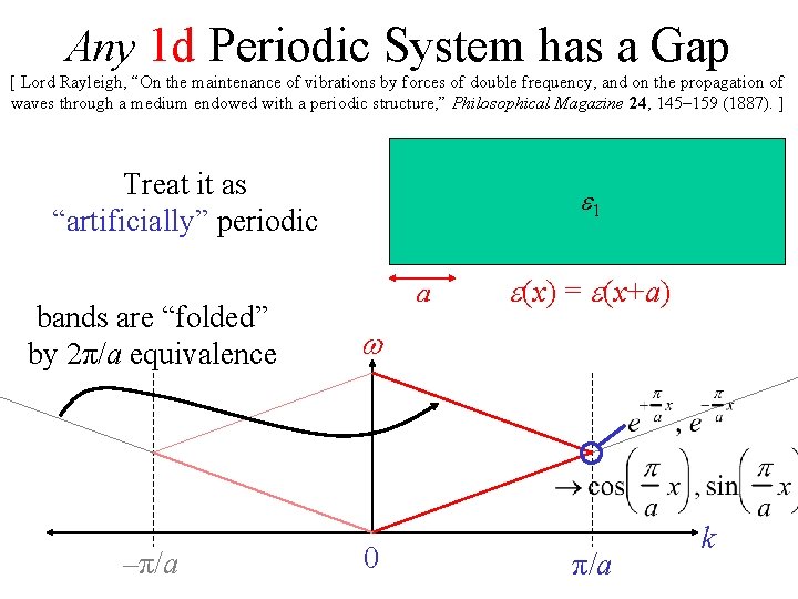
Periodic Hermitian Eigenproblems in 1 d e 1 e 2 e 1 e 2 a e(x) = e(x+a) Consider k+2π/a: k is periodic: k + 2π/a equivalent to k “quasi-phase-matching” periodic! satisfies same equation as Hk = Hk

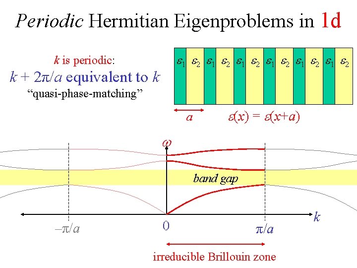
Periodic Hermitian Eigenproblems in 1 d e 1 e 2 e 1 e 2 k is periodic: k + 2π/a equivalent to k “quasi-phase-matching” a e(x) = e(x+a) w band gap –π/a 0 π/a irreducible Brillouin zone k

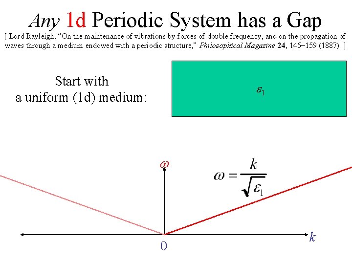
Any 1 d Periodic System has a Gap [ Lord Rayleigh, “On the maintenance of vibrations by forces of double frequency, and on the propagation of waves through a medium endowed with a periodic structure, ” Philosophical Magazine 24, 145– 159 (1887). ] Start with a uniform (1 d) medium: e 1 w 0 k

Any 1 d Periodic System has a Gap [ Lord Rayleigh, “On the maintenance of vibrations by forces of double frequency, and on the propagation of waves through a medium endowed with a periodic structure, ” Philosophical Magazine 24, 145– 159 (1887). ] Treat it as “artificially” periodic bands are “folded” by 2π/a equivalence –π/a e 1 a e(x) = e(x+a) w 0 π/a k

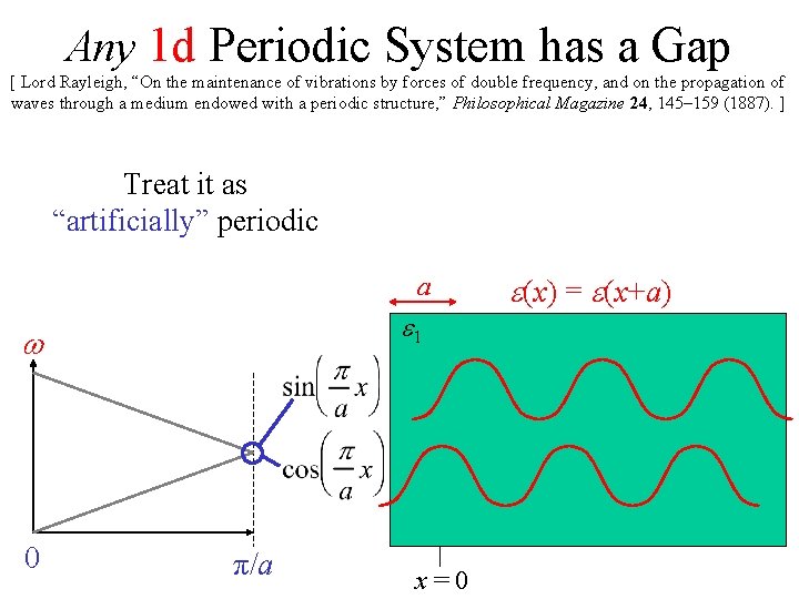
Any 1 d Periodic System has a Gap [ Lord Rayleigh, “On the maintenance of vibrations by forces of double frequency, and on the propagation of waves through a medium endowed with a periodic structure, ” Philosophical Magazine 24, 145– 159 (1887). ] Treat it as “artificially” periodic a e 1 w 0 π/a x = 0 e(x) = e(x+a)

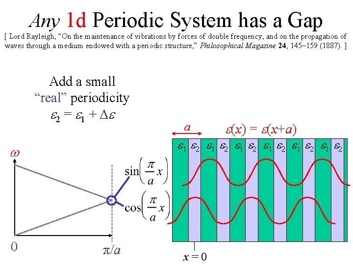
Any 1 d Periodic System has a Gap [ Lord Rayleigh, “On the maintenance of vibrations by forces of double frequency, and on the propagation of waves through a medium endowed with a periodic structure, ” Philosophical Magazine 24, 145– 159 (1887). ] Add a small “real” periodicity e 2 = e 1 + De e(x) = e(x+a) e 1 e 2 e 1 e 2 w 0 a π/a x = 0

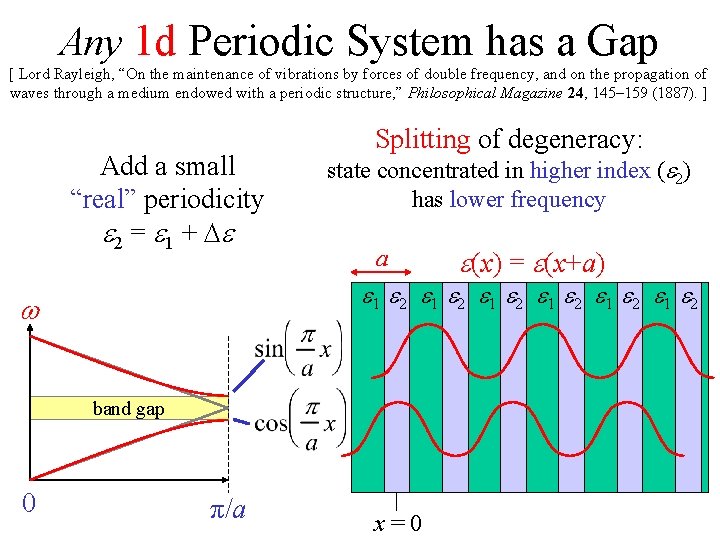
Any 1 d Periodic System has a Gap [ Lord Rayleigh, “On the maintenance of vibrations by forces of double frequency, and on the propagation of waves through a medium endowed with a periodic structure, ” Philosophical Magazine 24, 145– 159 (1887). ] Add a small “real” periodicity e 2 = e 1 + De Splitting of degeneracy: state concentrated in higher index (e 2) has lower frequency a e 1 e 2 e 1 e 2 w band gap 0 e(x) = e(x+a) π/a x = 0

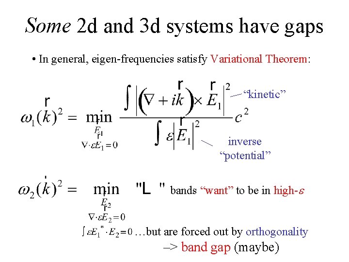
Some 2 d and 3 d systems have gaps • In general, eigen-frequencies satisfy Variational Theorem: “kinetic” inverse “potential” bands “want” to be in high-e …but are forced out by orthogonality –> band gap (maybe)

algebraic interlude completed… … I hope you were taking notes* [ *if not, see e. g. : Joannopoulos, Meade, and Winn, Photonic Crystals: Molding the Flow of Light ]

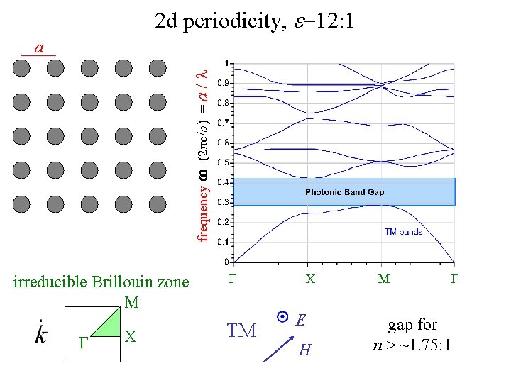
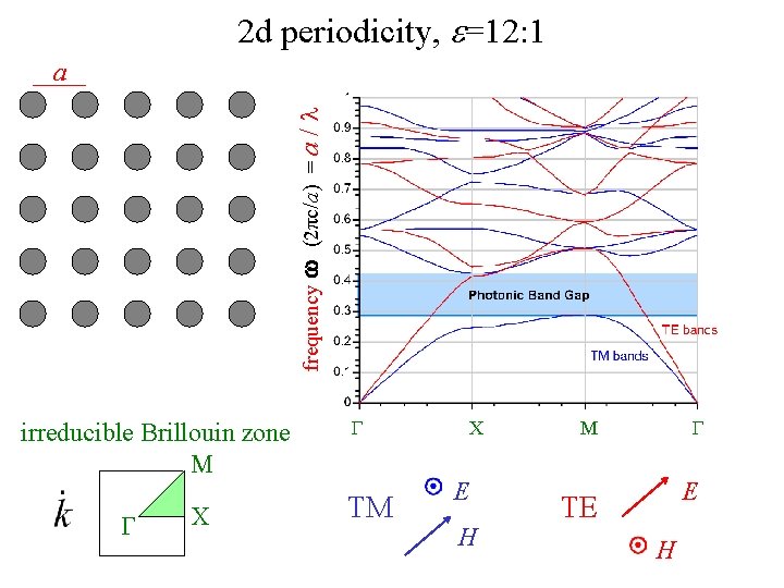
2 d periodicity, e=12: 1 frequency w (2πc/a) = a / a irreducible Brillouin zone M G X G TM X E H M G gap for n > ~1. 75: 1

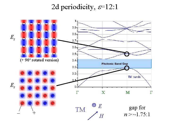
2 d periodicity, e=12: 1 Ez (+ 90° rotated version) Ez G – + TM X E H M G gap for n > ~1. 75: 1

2 d periodicity, e=12: 1 frequency w (2πc/a) = a / a irreducible Brillouin zone M G X G TM X E H G M E TE H

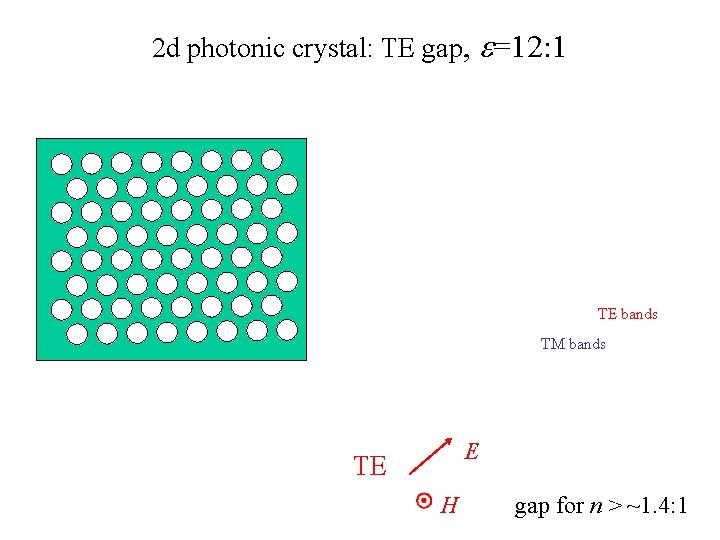
2 d photonic crystal: TE gap, e=12: 1 TE bands TM bands E TE H gap for n > ~1. 4: 1

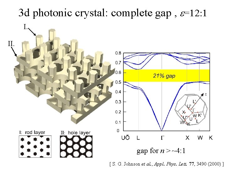
3 d photonic crystal: complete gap , e=12: 1 I. II. gap for n > ~4: 1 [ S. G. Johnson et al. , Appl. Phys. Lett. 77, 3490 (2000) ]

You, too, can compute photonic eigenmodes! MIT Photonic-Bands (MPB) package: http: //ab-initio. mit. edu/mpb on Athena: add mpb