Contents Implementation Technologies Standard chips PLD ASIC Xilinx




- Slides: 69


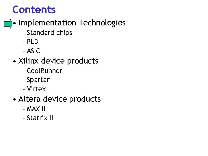
Contents • Implementation Technologies - Standard chips - PLD - ASIC • Xilinx device products - Cool. Runner - Spartan - Virtex • Altera device products - MAX II - Statrix II

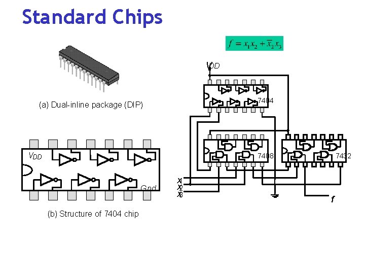
Standard Chips VDD 7404 (a) Dual-inline package (DIP) VDD 7408 Gnd (b) Structure of 7404 chip x 1 x 2 x 3 7432 f

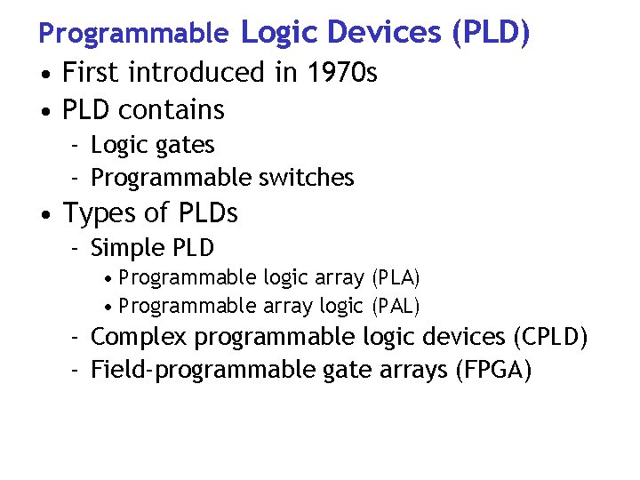
Programmable Logic Devices (PLD) • First introduced in 1970 s • PLD contains - Logic gates - Programmable switches • Types of PLDs - Simple PLD • Programmable logic array (PLA) • Programmable array logic (PAL) - Complex programmable logic devices (CPLD) - Field-programmable gate arrays (FPGA)

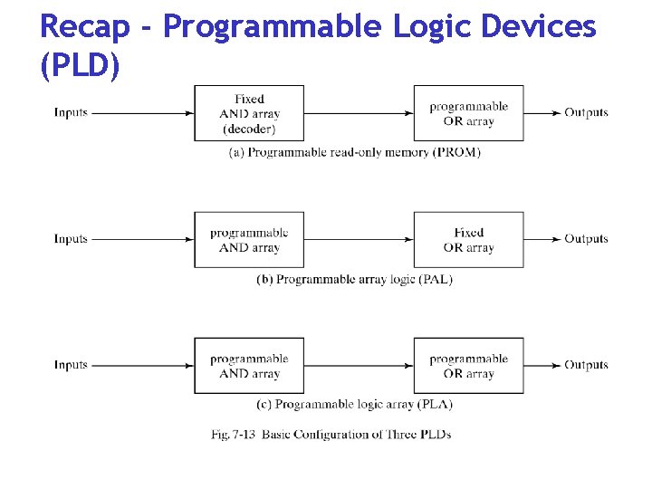
Recap - Programmable Logic Devices (PLD)

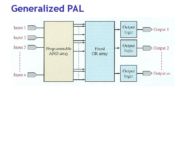
Generalized PAL

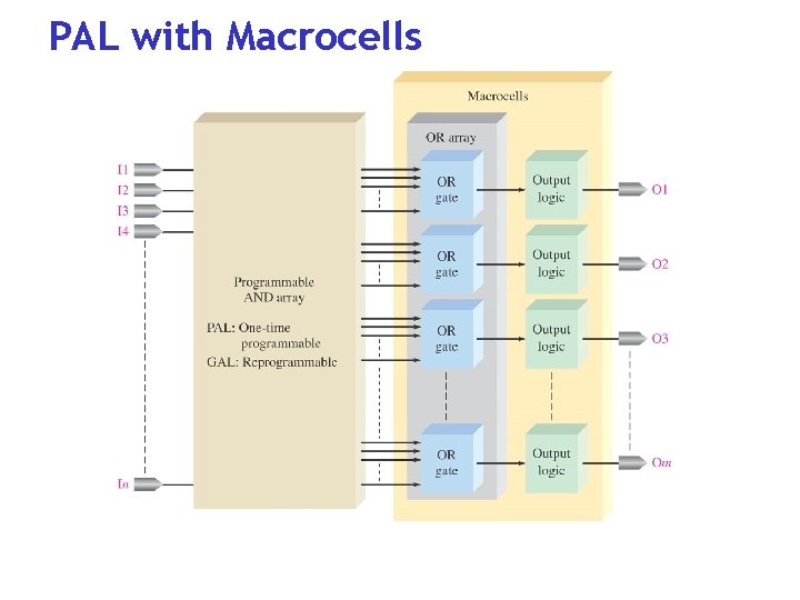
Programmable Logic Device (PLD) • Simple PLD (SPLD) & Complex PLD • SPLD - PAL itself is considered as SPLD - The fixed part (the blue part of the previous slide) is called “Macrocells” - A macrocell is with one OR gate and associated output logic. - A typical SPLD has 8~10 macrocells within one IC package.

PAL with Macrocells

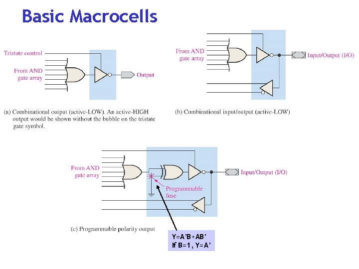
Basic Macrocells Y=A’B+AB’ If B=1, Y=A’

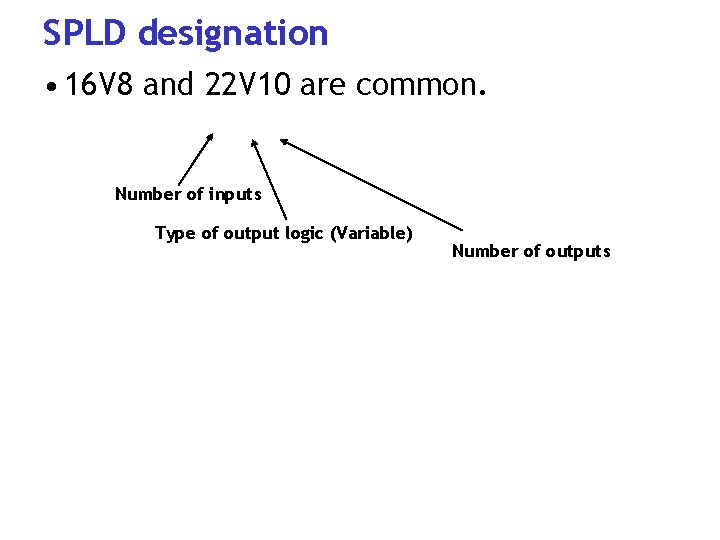
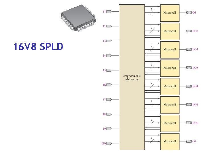
SPLD designation • 16 V 8 and 22 V 10 are common. Number of inputs Type of output logic (Variable) Number of outputs

16 V 8 SPLD

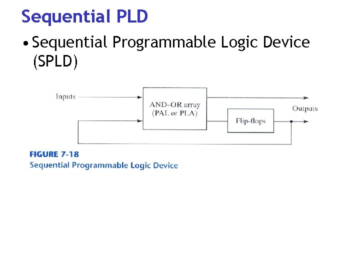
Sequential PLD • Sequential Programmable Logic Device (SPLD)

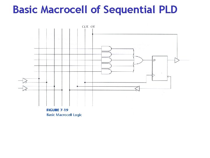
Basic Macrocell of Sequential PLD

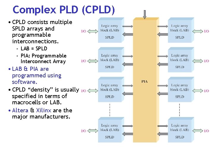
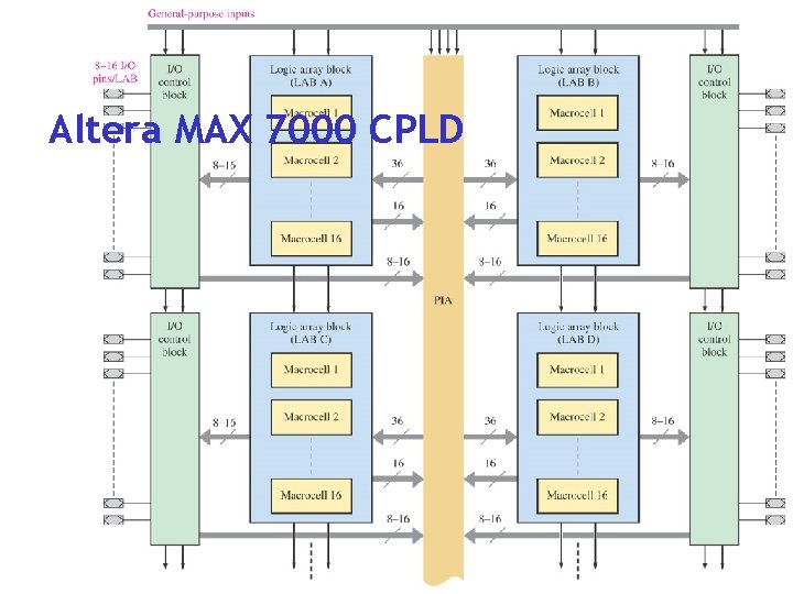
Complex PLD (CPLD) • CPLD consists multiple SPLD arrays and programmable interconnections. - LAB = SPLD - PIA: Programmable Interconnect Array • LAB & PIA are programmed using software. • CPLD “density” is usually specified in terms of macrocells or LAB. • Altera & Xilinx are the major manufacturers.

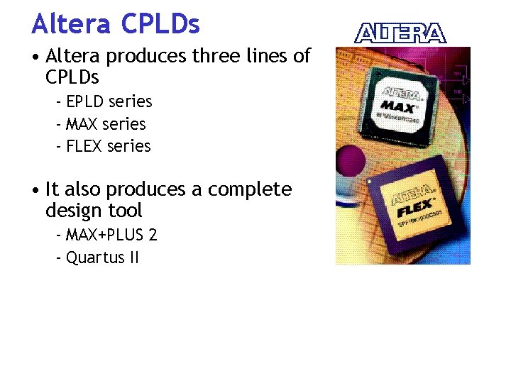
Altera CPLDs • Altera produces three lines of CPLDs - EPLD series - MAX series - FLEX series • It also produces a complete design tool - MAX+PLUS 2 - Quartus II

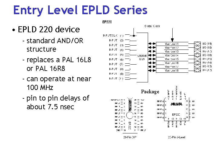
Entry Level EPLD Series • EPLD 220 device - standard AND/OR structure - replaces a PAL 16 L 8 or PAL 16 R 8 - can operate at near 100 MHz - pin to pin delays of about 7. 5 nsec Package

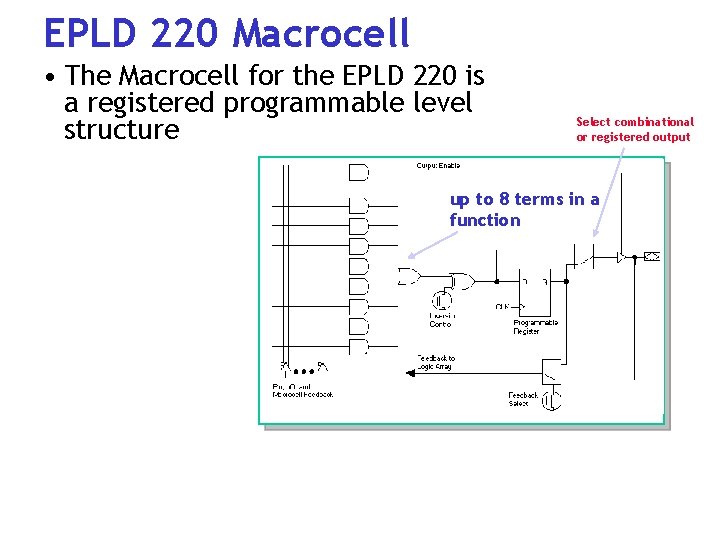
EPLD 220 Macrocell • The Macrocell for the EPLD 220 is a registered programmable level structure Select combinational or registered output up to 8 terms in a function

Altera MAX 7000 CPLD

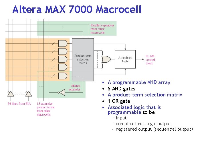
Altera MAX 7000 Macrocell • • • A programmable AND array 5 AND gates A product-term selection matrix 1 OR gate Associated logic that is programmable to be - input - combinational logic output - registered output (sequential output)

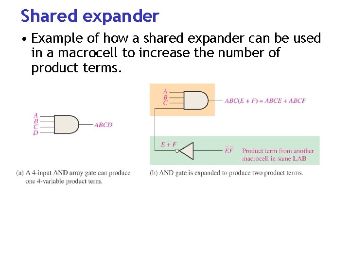
Shared expander • Example of how a shared expander can be used in a macrocell to increase the number of product terms.

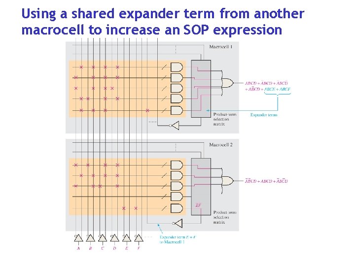
Using a shared expander term from another macrocell to increase an SOP expression

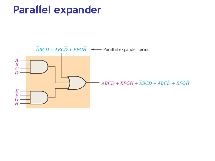
Parallel expander

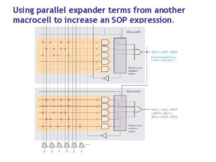
Using parallel expander terms from another macrocell to increase an SOP expression.

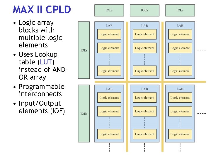
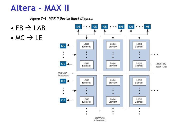
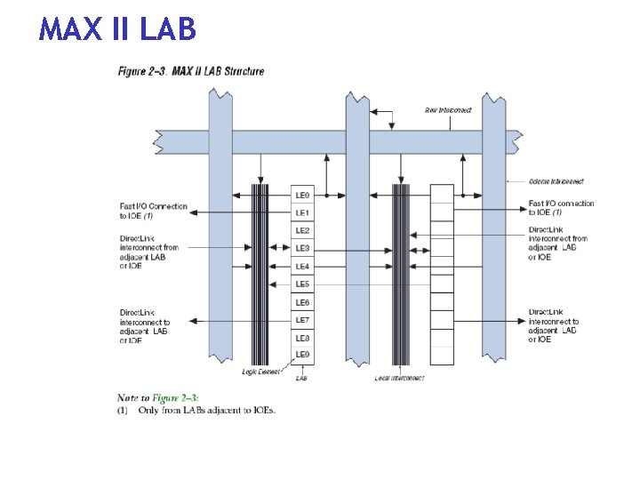
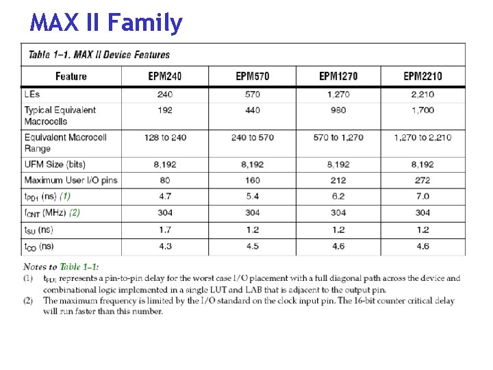
MAX II CPLD • Logic array blocks with multiple logic elements • Uses Lookup table (LUT) instead of ANDOR array • Programmable interconnects • Input/Output elements (IOE)

Xilinx CPLDs • Cool. Runner II, XC 9500 • XC 9500 is similar to MAX 7000, has PAL architecture • Cool. Runner II has PLA architecture

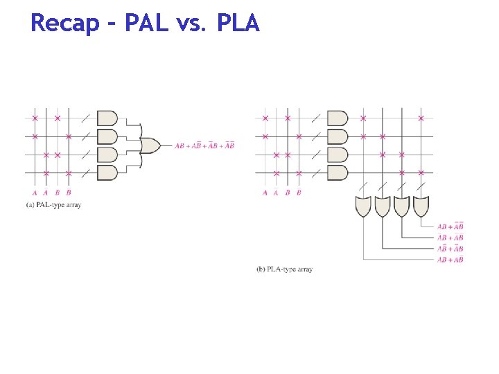
Recap – PAL vs. PLA

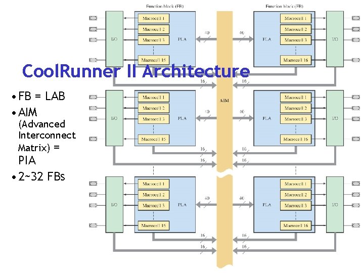
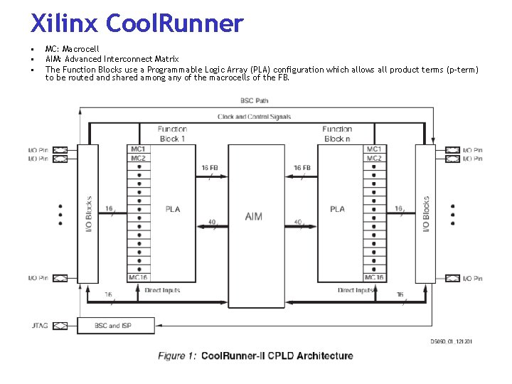
Cool. Runner II Architecture • FB = LAB • AIM (Advanced Interconnect Matrix) = PIA • 2~32 FBs

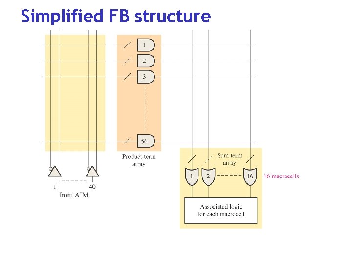
Simplified FB structure

FPGA • Provides logic blocks instead of AND or NAND plane - Typical logic blocks is LUT • Volatile devices - Programmable read-only memory (PROM) can be used to make it nonvolatile

LUT as Logic Block 3 -input LUT x 1 x 2 0/1 0/1 x 3 Program is actually written in Memory, just like conventional CPU with Main Memory. f

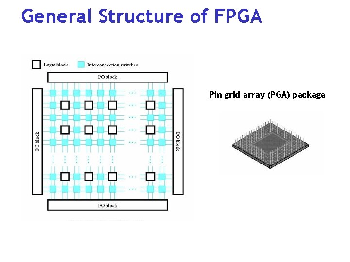
General Structure of FPGA Pin grid array (PGA) package

FPGA Example f 1 f 2

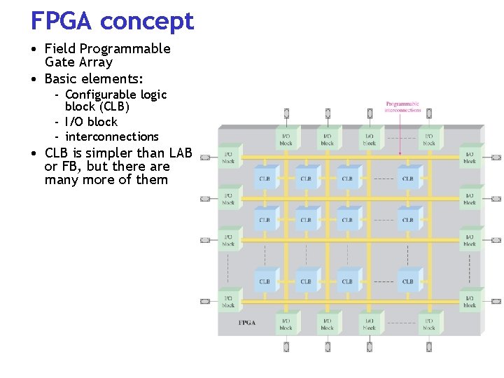
FPGA concept • Field Programmable Gate Array • Basic elements: - Configurable logic block (CLB) - I/O block - interconnections • CLB is simpler than LAB or FB, but there are many more of them

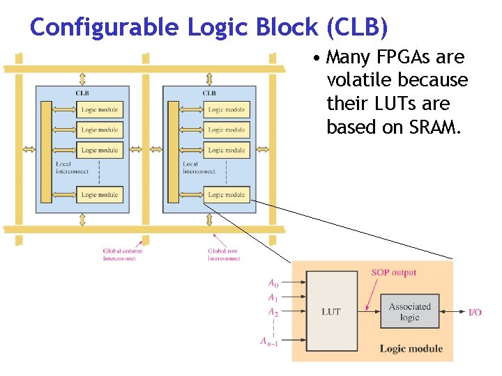
Configurable Logic Block (CLB) • Many FPGAs are volatile because their LUTs are based on SRAM.

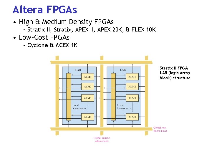
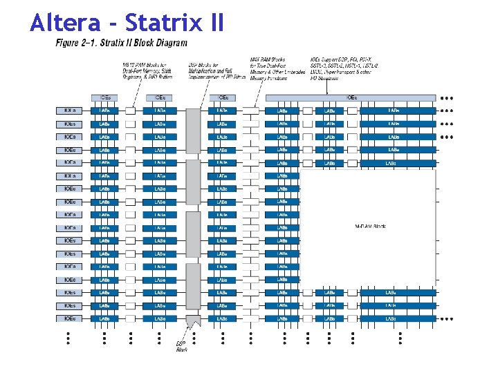
Altera FPGAs • High & Medium Density FPGAs - Stratix II, Stratix, APEX II, APEX 20 K, & FLEX 10 K • Low-Cost FPGAs - Cyclone & ACEX 1 K Stratix II FPGA LAB (logic array block) structure

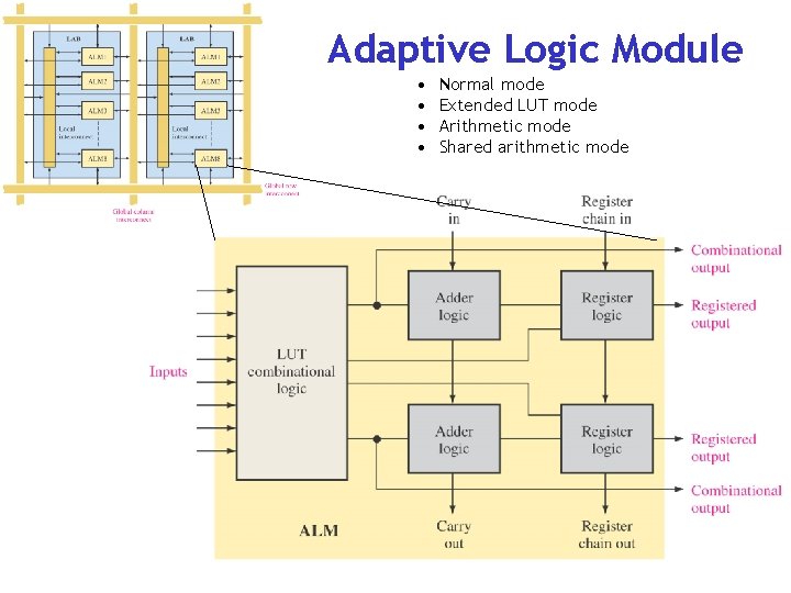
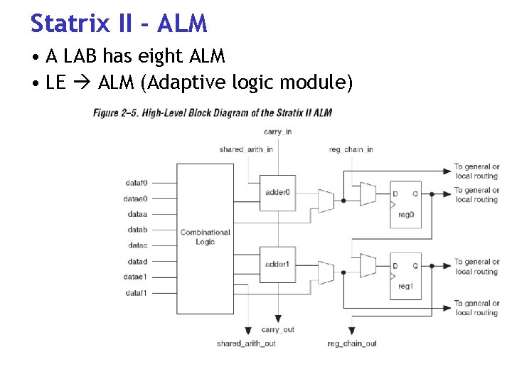
Adaptive Logic Module • • Normal mode Extended LUT mode Arithmetic mode Shared arithmetic mode

ASIC • Application-specific integrated circuit - Smallest size - Fastest speed - Lowest power • Microprocessors or memory chips - Not standard • Types of ASIC - Custom chips - Standard cell chips - Gate array

Standard Cell Chips • Use the pre-designed layout of individual gates • CAD tools arranges all the gates

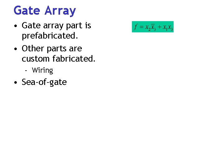
Gate Array • Gate array part is prefabricated. • Other parts are custom fabricated. - Wiring • Sea-of-gate

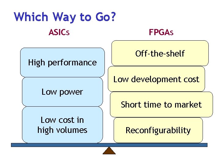
Which Way to Go? ASICs High performance FPGAs Off-the-shelf Low development cost Low power Short time to market Low cost in high volumes Reconfigurability

Other FPGA Advantages • Manufacturing cycle for ASIC is very costly, lengthy and engages lots of manpower - Mistakes not detected at design time, which have large impact on development time and cost - FPGAs are perfect for rapid prototyping of digital circuits • Easy upgrades like in case of software • Unique applications - reconfigurable computing

Major FPGA Vendors SRAM-based FPGAs • Xilinx, Inc. Share over 60% of the market • Altera Corp. • Atmel • Lattice Semiconductor Flash & antifuse FPGAs • Actel Corp. • Quick Logic Corp.

Contents • Implementation Technologies - Standard chips - PLD - ASIC • Xilinx device products - Cool. Runner - Spartan - Virtex • Altera device products - MAX II - Statrix II

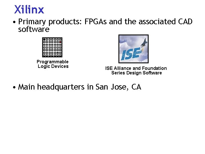
Xilinx • Primary products: FPGAs and the associated CAD software Programmable Logic Devices ISE Alliance and Foundation Series Design Software • Main headquarters in San Jose, CA

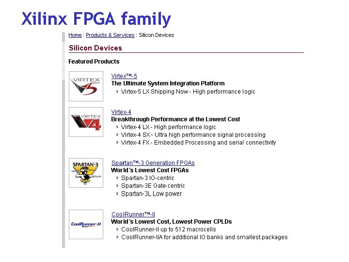
Xilinx FPGA family

Xilinx Cool. Runner • • • MC: Macrocell AIM: Advanced Interconnect Matrix The Function Blocks use a Programmable Logic Array (PLA) configuration which allows all product terms (p-term) to be routed and shared among any of the macrocells of the FB.

Cool. Runner Macrocell

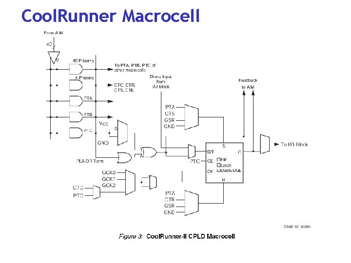
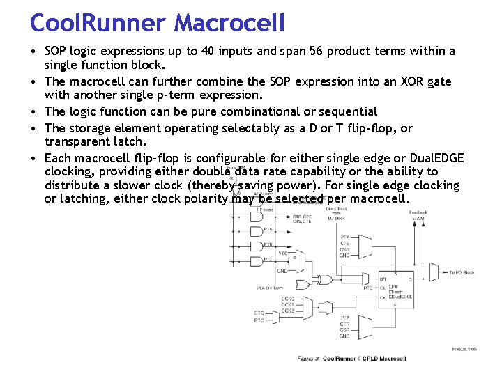
Cool. Runner Macrocell • SOP logic expressions up to 40 inputs and span 56 product terms within a single function block. • The macrocell can further combine the SOP expression into an XOR gate with another single p-term expression. • The logic function can be pure combinational or sequential • The storage element operating selectably as a D or T flip-flop, or transparent latch. • Each macrocell flip-flop is configurable for either single edge or Dual. EDGE clocking, providing either double data rate capability or the ability to distribute a slower clock (thereby saving power). For single edge clocking or latching, either clock polarity may be selected per macrocell.

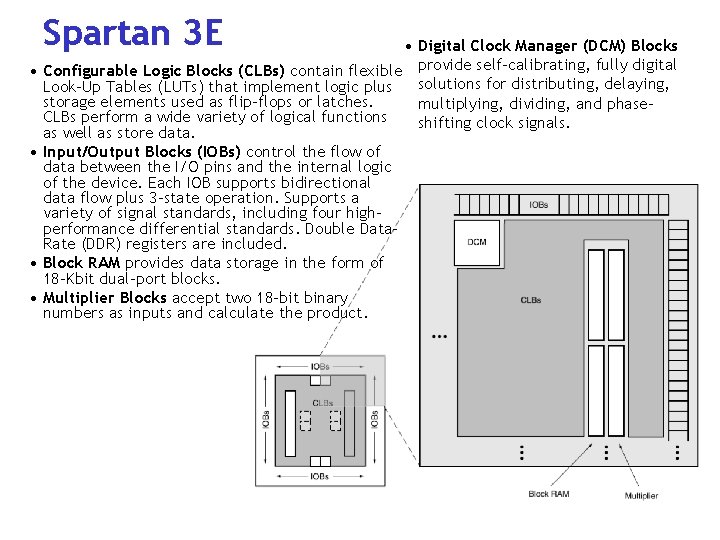
Spartan 3 E • • • Digital Clock Manager (DCM) Blocks Configurable Logic Blocks (CLBs) contain flexible provide self-calibrating, fully digital solutions for distributing, delaying, Look-Up Tables (LUTs) that implement logic plus storage elements used as flip-flops or latches. multiplying, dividing, and phase. CLBs perform a wide variety of logical functions shifting clock signals. as well as store data. Input/Output Blocks (IOBs) control the flow of data between the I/O pins and the internal logic of the device. Each IOB supports bidirectional data flow plus 3 -state operation. Supports a variety of signal standards, including four highperformance differential standards. Double Data. Rate (DDR) registers are included. Block RAM provides data storage in the form of 18 -Kbit dual-port blocks. Multiplier Blocks accept two 18 -bit binary numbers as inputs and calculate the product.

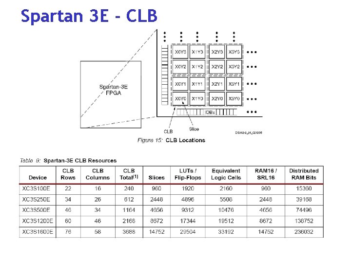
Spartan 3 E - CLB

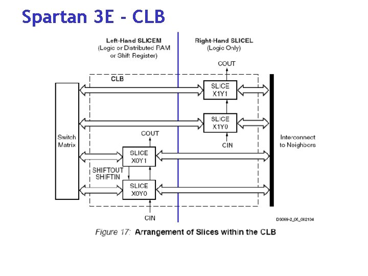
Spartan 3 E - CLB

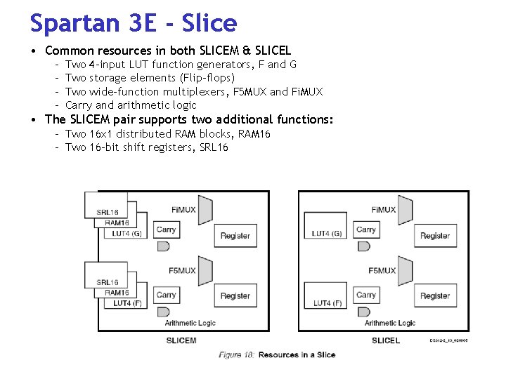
Spartan 3 E - Slice • Common resources in both SLICEM & SLICEL - Two 4 -input LUT function generators, F and G Two storage elements (Flip-flops) Two wide-function multiplexers, F 5 MUX and Fi. MUX Carry and arithmetic logic • The SLICEM pair supports two additional functions: - Two 16 x 1 distributed RAM blocks, RAM 16 - Two 16 -bit shift registers, SRL 16

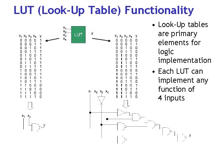
LUT (Look-Up Table) Functionality • Look-Up tables are primary elements for logic implementation • Each LUT can implement any function of 4 inputs

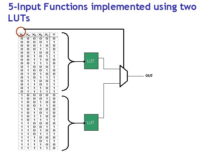
5 -Input Functions implemented using two LUTs LUT OUT LUT

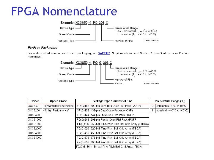
FPGA Nomenclature

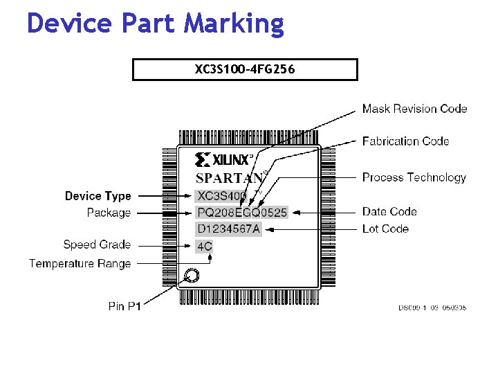
Device Part Marking XC 3 S 100 -4 FG 256

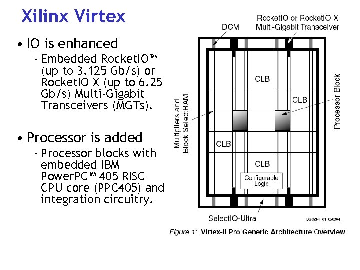
Xilinx Virtex • IO is enhanced - Embedded Rocket. IO™ (up to 3. 125 Gb/s) or Rocket. IO X (up to 6. 25 Gb/s) Multi-Gigabit Transceivers (MGTs). • Processor is added - Processor blocks with embedded IBM Power. PC™ 405 RISC CPU core (PPC 405) and integration circuitry.

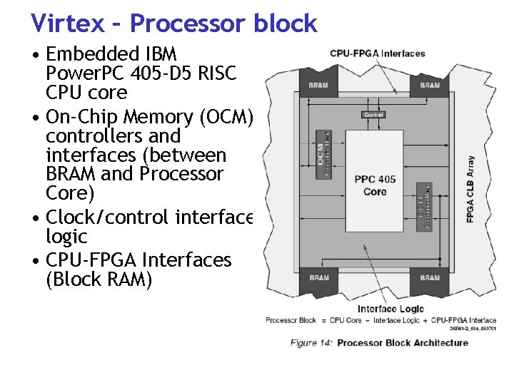
Virtex – Processor block • Embedded IBM Power. PC 405 -D 5 RISC CPU core • On-Chip Memory (OCM) controllers and interfaces (between BRAM and Processor Core) • Clock/control interface logic • CPU-FPGA Interfaces (Block RAM)

Contents • Implementation Technologies - Standard chips - PLD - ASIC • Xilinx device products - Cool. Runner - Spartan - Virtex • Altera device products - MAX II - Statrix II

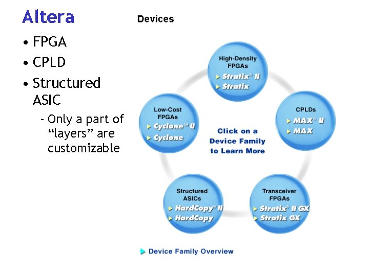
Altera • FPGA • CPLD • Structured ASIC - Only a part of “layers” are customizable

Altera – MAX II • FB LAB • MC LE

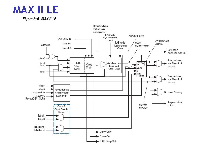
MAX II LE

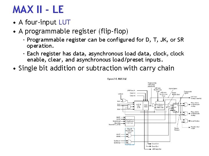
MAX II - LE • A four-input LUT • A programmable register (flip-flop) - Programmable register can be configured for D, T, JK, or SR operation. - Each register has data, asynchronous load data, clock enable, clear, and asynchronous load/preset inputs. • Single bit addition or subtraction with carry chain

MAX II LAB

MAX II Family

Altera - Statrix II

Statrix II - ALM • A LAB has eight ALM • LE ALM (Adaptive logic module)

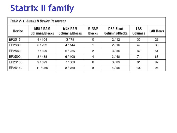
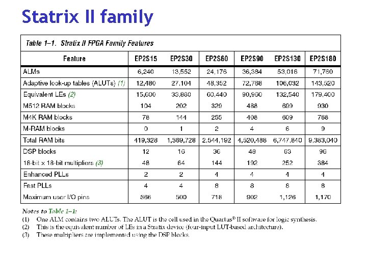
Statrix II family

Statrix II family